EP1096026A2 - Method of manufacturing thin metal alloy foils - Google Patents
Method of manufacturing thin metal alloy foils Download PDFInfo
- Publication number
- EP1096026A2 EP1096026A2 EP00308786A EP00308786A EP1096026A2 EP 1096026 A2 EP1096026 A2 EP 1096026A2 EP 00308786 A EP00308786 A EP 00308786A EP 00308786 A EP00308786 A EP 00308786A EP 1096026 A2 EP1096026 A2 EP 1096026A2
- Authority
- EP
- European Patent Office
- Prior art keywords
- metal
- sacrificial layer
- foil
- alloy
- carrier surface
- Prior art date
- Legal status (The legal status is an assumption and is not a legal conclusion. Google has not performed a legal analysis and makes no representation as to the accuracy of the status listed.)
- Withdrawn
Links
Images

Classifications
-
- C—CHEMISTRY; METALLURGY
- C01—INORGANIC CHEMISTRY
- C01B—NON-METALLIC ELEMENTS; COMPOUNDS THEREOF; METALLOIDS OR COMPOUNDS THEREOF NOT COVERED BY SUBCLASS C01C
- C01B3/00—Hydrogen; Gaseous mixtures containing hydrogen; Separation of hydrogen from mixtures containing it; Purification of hydrogen; Reversible storage of hydrogen
- C01B3/50—Separation of hydrogen or hydrogen-containing gases from gaseous mixtures, e.g. purification
- C01B3/501—Separation of hydrogen or hydrogen-containing gases from gaseous mixtures, e.g. purification by diffusion
- C01B3/503—Separation of hydrogen or hydrogen-containing gases from gaseous mixtures, e.g. purification by diffusion characterised by membranes
- C01B3/505—Membranes containing palladium
-
- B—PERFORMING OPERATIONS; TRANSPORTING
- B32—LAYERED PRODUCTS
- B32B—LAYERED PRODUCTS, i.e. PRODUCTS BUILT-UP OF STRATA OF FLAT OR NON-FLAT, e.g. CELLULAR OR HONEYCOMB, FORM
- B32B15/00—Layered products comprising a layer of metal
- B32B15/01—Layered products comprising a layer of metal all layers being exclusively metallic
-
- C—CHEMISTRY; METALLURGY
- C22—METALLURGY; FERROUS OR NON-FERROUS ALLOYS; TREATMENT OF ALLOYS OR NON-FERROUS METALS
- C22C—ALLOYS
- C22C1/00—Making non-ferrous alloys
-
- C—CHEMISTRY; METALLURGY
- C23—COATING METALLIC MATERIAL; COATING MATERIAL WITH METALLIC MATERIAL; CHEMICAL SURFACE TREATMENT; DIFFUSION TREATMENT OF METALLIC MATERIAL; COATING BY VACUUM EVAPORATION, BY SPUTTERING, BY ION IMPLANTATION OR BY CHEMICAL VAPOUR DEPOSITION, IN GENERAL; INHIBITING CORROSION OF METALLIC MATERIAL OR INCRUSTATION IN GENERAL
- C23C—COATING METALLIC MATERIAL; COATING MATERIAL WITH METALLIC MATERIAL; SURFACE TREATMENT OF METALLIC MATERIAL BY DIFFUSION INTO THE SURFACE, BY CHEMICAL CONVERSION OR SUBSTITUTION; COATING BY VACUUM EVAPORATION, BY SPUTTERING, BY ION IMPLANTATION OR BY CHEMICAL VAPOUR DEPOSITION, IN GENERAL
- C23C14/00—Coating by vacuum evaporation, by sputtering or by ion implantation of the coating forming material
- C23C14/0005—Separation of the coating from the substrate
-
- Y—GENERAL TAGGING OF NEW TECHNOLOGICAL DEVELOPMENTS; GENERAL TAGGING OF CROSS-SECTIONAL TECHNOLOGIES SPANNING OVER SEVERAL SECTIONS OF THE IPC; TECHNICAL SUBJECTS COVERED BY FORMER USPC CROSS-REFERENCE ART COLLECTIONS [XRACs] AND DIGESTS
- Y10—TECHNICAL SUBJECTS COVERED BY FORMER USPC
- Y10S—TECHNICAL SUBJECTS COVERED BY FORMER USPC CROSS-REFERENCE ART COLLECTIONS [XRACs] AND DIGESTS
- Y10S55/00—Gas separation
- Y10S55/05—Methods of making filter
-
- Y—GENERAL TAGGING OF NEW TECHNOLOGICAL DEVELOPMENTS; GENERAL TAGGING OF CROSS-SECTIONAL TECHNOLOGIES SPANNING OVER SEVERAL SECTIONS OF THE IPC; TECHNICAL SUBJECTS COVERED BY FORMER USPC CROSS-REFERENCE ART COLLECTIONS [XRACs] AND DIGESTS
- Y10—TECHNICAL SUBJECTS COVERED BY FORMER USPC
- Y10T—TECHNICAL SUBJECTS COVERED BY FORMER US CLASSIFICATION
- Y10T428/00—Stock material or miscellaneous articles
- Y10T428/12—All metal or with adjacent metals
- Y10T428/12431—Foil or filament smaller than 6 mils
- Y10T428/12438—Composite
-
- Y—GENERAL TAGGING OF NEW TECHNOLOGICAL DEVELOPMENTS; GENERAL TAGGING OF CROSS-SECTIONAL TECHNOLOGIES SPANNING OVER SEVERAL SECTIONS OF THE IPC; TECHNICAL SUBJECTS COVERED BY FORMER USPC CROSS-REFERENCE ART COLLECTIONS [XRACs] AND DIGESTS
- Y10—TECHNICAL SUBJECTS COVERED BY FORMER USPC
- Y10T—TECHNICAL SUBJECTS COVERED BY FORMER US CLASSIFICATION
- Y10T428/00—Stock material or miscellaneous articles
- Y10T428/12—All metal or with adjacent metals
- Y10T428/12493—Composite; i.e., plural, adjacent, spatially distinct metal components [e.g., layers, joint, etc.]
- Y10T428/12771—Transition metal-base component
- Y10T428/12861—Group VIII or IB metal-base component
- Y10T428/12875—Platinum group metal-base component
-
- Y—GENERAL TAGGING OF NEW TECHNOLOGICAL DEVELOPMENTS; GENERAL TAGGING OF CROSS-SECTIONAL TECHNOLOGIES SPANNING OVER SEVERAL SECTIONS OF THE IPC; TECHNICAL SUBJECTS COVERED BY FORMER USPC CROSS-REFERENCE ART COLLECTIONS [XRACs] AND DIGESTS
- Y10—TECHNICAL SUBJECTS COVERED BY FORMER USPC
- Y10T—TECHNICAL SUBJECTS COVERED BY FORMER US CLASSIFICATION
- Y10T428/00—Stock material or miscellaneous articles
- Y10T428/12—All metal or with adjacent metals
- Y10T428/12493—Composite; i.e., plural, adjacent, spatially distinct metal components [e.g., layers, joint, etc.]
- Y10T428/12771—Transition metal-base component
- Y10T428/12861—Group VIII or IB metal-base component
- Y10T428/12903—Cu-base component
Definitions
- the present invention is directed to a method of manufacturing thin metal alloy foils using evaporative techniques. More specifically, the present invention is directed to manufacturing metal alloy foils by depositing layers of different metals and heating the layers to form the alloy.
- separators for chemical components.
- This invention will be described as a method of manufacturing a thin metal foil that may be used as a separator.
- the separator is exposed to a mixed gas stream on one surface.
- the separator material allows one component of the gas stream to pass through the material and separate one selected gas at very high concentration from the mixed gas stream.
- Metal separators have been used to separate hydrogen from a gas stream containing hydrogen and other gases.
- Hydrogen separators generally operate by catalysing the hydrogen gas into hydrogen atoms that selectively pass through the foil. The hydrogen atoms recombine on the opposite surface of the foil to form hydrogen gas.
- the permeability of the separator increases as the foil thickness decreases. Thin metal foils are much more efficient in separating hydrogen gas than thicker foils.
- the metal foils have been made by a rolling or pressing technique.
- An ingot of metal having a desired composition is cast and rolled or pressed into a foil.
- This rolling or pressing technique is only capable of producing a consistently pinhole free foil having a thickness not less than 25 microns.
- the foil may tear and have pinholes when it is rolled to a thickness less than 25 microns.
- the metal alloy has superior physical properties such as non-embrittlement, and may be more effective at separating one component from a mixed gas stream.
- the metal alloy has traditionally been formed by blending metal powders or shots and then heating the mixture to melt the metals. The molten metals blend and form an alloy when cooled. The alloy ingot is then rolled or pressed to form the thin metal foil.
- the problem with rolling the alloy is that it takes many successive "rolls and anneals" to produce a thin film.
- An ingot of an alloy cannot be rolled down to the desired thickness in one trial.
- the ingot is rolled down a few millimetres at a time with an anneal in between each rolling action.
- Electroless plating is an example of an electrochemically deposited metal.
- the problem with electroless plating is that it introduces unwanted elements to the material.
- the present invention is intended to produce self supporting foils that will be used independently from the carrier and have a high degree of elemental purity.
- a method of manufacturing thin alloy foil comprising the steps of: providing a carrier having a surface; applying a first metal layer atop said carrier surface; applying a second metal layer atop said first layer; removing said first and second metal layers from said carrier surface; and alloying said first and second metal layers to form said alloy foil.
- the present invention attempts to provide a method of manufacturing thin alloy foils that does not utilise a rolling or pressing process.
- the method enables the manufacture of very thin foils having metallurgical compositions not attainable through conventional alloying methods.
- the embodiment of the present invention provides a method of manufacturing thin foil alloys through a series of steps.
- a carrier having a polished carrier surface is placed within a deposition chamber.
- a sacrificial layer is applied atop the carrier surface.
- the sacrificial layer is made of a material that may be easily dissolved or separated from the carrier surface to remove the metal foil.
- Suitable sacrificial layers include common photo resist layers used in electrical circuit board manufacturing.
- the carrier surface and sacrificial layer are placed within the deposition chamber.
- the sacrificial layer is exposed to an evaporated first metal which becomes deposited upon the sacrificial layer.
- An evaporated second metal is then applied concurrently or sequentially with the first metal.
- the first and second evaporated metals solidify on the sacrificial layer to form a multilayer foil.
- the multilayer foil includes discrete layers or areas of the evaporated metals.
- the carrier, sacrificial layer, and multilayer foil are bathed with a solvent to dissolve the sacrificial layer.
- the multilayer foil is removed from the carrier surface.
- the multilayer foil is placed within a reducing atmosphere and exposed to elevated temperatures.
- the multilayer foil forms an alloy of the deposited metals.
- the method described enables the production of thin metal foils having a thickness of between 1 and 10 microns.
- the invention is especially useful for the production of foils of 5 microns or thinner. Micron foils of less than 1 micron have been produced. A foil less than 1 micron may be fabricated, but, may be difficult to use without tearing.
- the method enables the manufacture of foils made from dissimilar metals.
- the invention has been tested and will be described as a method of making thin metal foils for use as a hydrogen separator.
- alloys of palladium and copper were preferred.
- Other applications and other metal compositions are also possible using the methods described and claimed herein.
- metal compositions include, but are not limited to the following: Pd-Ag, Pd-Y, and V-Cu. These alloys may be used in optical, sensing, catalytic, and wear friction, applications.
- the invention will be illustrated and described as a method of making a thin metal foil.
- the foil is particularly useful in the manufacture of hydrogen separators.
- other metal foils particularly those requiring metal alloys may be manufactured using the method described.
- These and other devices and methods of manufacture are included within the invention described herein.
- the following items are a word list of the components described in the drawings and are reproduced to aid in understanding the invention:
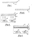
- the substrate 10 that will receive the evaporated metal.
- the substrate 10 is made from a 4 inch single crystal silicon polished wafer. However, any smooth substrate that has the mechanical characteristics of silicon may be used.
- the substrate 10 is polished to a mirrored surface finish of about 0.5 microns. A highly polished surface allows the sacrificial layer to be easily removed.
- the substrate may be flat to make foil sheets, or may be cylindrical to make tubular shaped metal foils.
- the substrate 10 has a substrate surface 12.
- the substrate surface 12 receives a sacrificial layer 14 as illustrated in Figure 2.
- the sacrificial layer 14 is a temporary layer that is easily removed to separate the metal foil from the substrate. Suitable sacrificial layers include wax, grease, oil, and photo resist.
- Photoresist is a photosensitive polymer commonly used in the electronics industry to apply chemically resistive patterns to silicon wafers. The manufacturer of the photoresist used in this application is Hoechst Celanese.
- the sacrificial layer 14 is created by spinning the substrate at a high rate and applying the photoresist.
- the photoresist is approximately 0.8 to 1.5 microns thick.
- the deposition chamber 16 may be an evaporative deposition, sputtering deposition, or chemical vapour deposition device.
- the air within the chamber 16 is removed to provide a mean free path for the evaporated material.
- a crucible 18 containing a first metal 20 is heated.
- the first metal 20 evaporates and deposits a first metal layer 22 atop the sacrificial layer 14 as illustrated in Figure 4.
- Concurrently or subsequent to the deposition of the first metal layer 22, a crucible 24 heats a second metal 26 and causes the second metal to evaporate.
- the second metal 26 deposits a second metal layer 28.
- the first and second metal layers 22, 28 form a multilayer foil 40 as illustrated in Figures 5 and 6.
- the multilayer foil 30 includes discrete layers for areas of the individual metals 20, 26.
- the multilayer foil 30 does not yet have the physical properties of an alloy.
- the substrate 10, sacrificial layer 14, and multilayer foil 30 are placed within a solvent bath to dissolve the sacrificial layer 14 and releases the multilayer foil 30 from the substrate 10.
- Acetone was found to be a suitable solvent for removing a photo resist sacrificial layer.
- the multilayer foil 30 is placed within a reducing atmosphere furnace as illustrated in Figure 6.
- the multilayer foil 30 is heated sufficiently to cause the first and second metal layers 22, 28 to form an alloy.
- An alloy is a metal that is prepared by adding other metals or non-metals to a basic metal to secure desirable properties. Usually alloying metals increases the hardness of the original base metal.
- the multilayer foil 30 is transformed into a self supporting thin alloy foil 32 as illustrated in Figure 7.
- the multilayer foil 30 is heated in a reducing atmosphere such as hydrogen.
- a reducing atmosphere such as hydrogen.
- An alloy foil having a composition of 60% palladium and 40% copper is desired.
- a 4-inch, single crystal silicon wafer acts as the substrate.
- the wafer is chem-mechanical polished to a surface flatness of +/- 6 micron.
- the wafer is placed within a holder rotating vacuum chuck.
- a photo resist of AZ1512 is spun onto the silicon wafer surface to form the sacrificial layer.
- the photo resist is applied by conventional spinning techniques and has a thickness of between 0.8 and 1 micron.
- the photo resist and photo resist is baked under a heat lamp for 20 minutes to evaporate the solvents in the photo resist.
- the photo resist hardens to a smooth finish without additional processing.
- a TEMESCAL electron beam metal evaporation system is used to evaporate the metal onto the surface of the photo resist.
- the silicon wafers are loaded into a planetary mechanism that rotates the silicon wafers during deposition. Rotating the wafers during deposition decreases the surface irregularities of the deposited metal.
- the copper was evaporated in increments of 5000 angstroms and the palladium was evaporated in increments of 4470 angstroms. A total thickness of 4.2 microns was evaporated.
- the silicon wafer was removed from the evaporation system and immersed in acetone.
- the multilayer foil immediately released from the silicon wafer to form a 4.2 micron thick multilayer foil.
- the multilayer foil was placed in a tube furnace for two hours at 800°C in a 3% hydrogen reducing atmosphere. The multilayer foil was transformed into a homogeneous uniform alloy.
- the alloy foil was analysed using x-ray diffraction analysis. The results indicate a homogeneous alloy structure. Quantitative composition analysis was performed using scanning electron microscope (SEM) energy dispersive spectroscopy (EDS). The results indicate a metal alloy having an elemental composition of 40.65% copper and 59.35% palladium. SEM photographs of the alloy foil indicate a tight, pin-hole free grain structure.
Landscapes
- Chemical & Material Sciences (AREA)
- Organic Chemistry (AREA)
- Engineering & Computer Science (AREA)
- Materials Engineering (AREA)
- Mechanical Engineering (AREA)
- Metallurgy (AREA)
- Chemical Kinetics & Catalysis (AREA)
- Combustion & Propulsion (AREA)
- Inorganic Chemistry (AREA)
- Physical Vapour Deposition (AREA)
Abstract
Description
- 10
- substrate
- 12
- substrate surface
- 14
- sacrificial layer
- 16
- deposition chamber
- 18
- crucible
- 20
- first metal
- 22
- second metal layer
- 24
- crucible
- 26
- second metal
- 28
- second metal layer
- 30
- multilayer foil
- 32
- metal alloy foil
Claims (10)
- A method of manufacturing thin alloy foil; comprising the steps of:providing a carrier (10) having a surface (12);applying a first metal layer (22) atop said carrier surface;applying a second metal layer (28) atop said first layer (22);removing said first and second metal layers (22,28) from said carrier surface; andalloying said first and second metal layers (22,28) to form said alloy foil.
- A method as claimed in claim 1, further comprising applying a sacrificial layer atop said carrier surface prior to said first metal layer application step.
- A method as claimed in claim 2, further comprising removing said sacrificial layer after said second metal layer application step and separating said first and second layers from said carrier surface.
- A method as claimed in any one of claims 1 to 3, wherein said first metal layer is selected from the metal group consisting of palladium and copper.
- A method as claimed in any one of the preceding claims, wherein said alloying step consists of heating said first and second metal layers.
- A method as claimed in claim 5, further comprising heating said first and second metal layers in a reducing atmosphere.
- A method as claimed in any one of the preceding claims, wherein said alloy foil has a thickness of between 1 and 5 microns.
- A method of manufacturing a hydrogen separator comprising the steps of:providing a carrier having a surface;applying a sacrificial layer atop said carrier surface;applying a first metal layer atop said carrier surface;applying a second metal layer atop said first layer;removing said sacrificial layer;removing said first and second metal layers from said carrier surface; andalloying said first and second metal layers to form said alloy foil.
- A hydrogen separator comprising a self supporting thin metal alloy having a thickness between 1 and 5 microns, said foil consisting essentially of an alloy of Pd and Cu.
- A separator as claimed in claim 9, wherein said alloy is approximately between 59% and 60% Pd and the balance Cu.
Applications Claiming Priority (2)
| Application Number | Priority Date | Filing Date | Title |
|---|---|---|---|
| US09/420,620 US6315820B1 (en) | 1999-10-19 | 1999-10-19 | Method of manufacturing thin metal alloy foils |
| US420620 | 1999-10-19 |
Publications (2)
| Publication Number | Publication Date |
|---|---|
| EP1096026A2 true EP1096026A2 (en) | 2001-05-02 |
| EP1096026A3 EP1096026A3 (en) | 2005-10-26 |
Family
ID=23667195
Family Applications (1)
| Application Number | Title | Priority Date | Filing Date |
|---|---|---|---|
| EP00308786A Withdrawn EP1096026A3 (en) | 1999-10-19 | 2000-10-05 | Method of manufacturing thin metal alloy foils |
Country Status (3)
| Country | Link |
|---|---|
| US (1) | US6315820B1 (en) |
| EP (1) | EP1096026A3 (en) |
| JP (1) | JP2001172732A (en) |
Cited By (5)
| Publication number | Priority date | Publication date | Assignee | Title |
|---|---|---|---|---|
| WO2007118527A1 (en) * | 2006-04-13 | 2007-10-25 | Imi Intelligent Medical Implants Ag | Method for producing implant structures for contacting or electrically stimulating living tissue cells or nerves |
| US8101243B2 (en) | 2002-04-03 | 2012-01-24 | Colorado School Of Mines | Method of making sulfur-resistant composite metal membranes |
| US8119205B2 (en) | 2002-04-03 | 2012-02-21 | Colorado School Of Mines | Process for preparing palladium alloy composite membranes for use in hydrogen separation, palladium alloy composite membranes and products incorporating or made from the membranes |
| US8778058B2 (en) | 2010-07-16 | 2014-07-15 | Colorado School Of Mines | Multilayer sulfur-resistant composite metal membranes and methods of making and repairing the same |
| US9044715B2 (en) | 2007-08-22 | 2015-06-02 | Colorado School Of Mines | Unsupported palladium alloy membranes and methods of making same |
Families Citing this family (19)
| Publication number | Priority date | Publication date | Assignee | Title |
|---|---|---|---|---|
| DE10039596C2 (en) * | 2000-08-12 | 2003-03-27 | Omg Ag & Co Kg | Supported metal membrane, process for its manufacture and use |
| JP3882567B2 (en) * | 2000-11-24 | 2007-02-21 | 住友電気工業株式会社 | Material separation structure |
| US6540850B2 (en) * | 2001-05-03 | 2003-04-01 | Ford Motor Company | Membrane and a method for making a membrane |
| JP2004008966A (en) * | 2002-06-07 | 2004-01-15 | Mitsubishi Heavy Ind Ltd | Hydrogen separating membrane, hydrogen separating unit and method for manufacturing the membrane |
| US7077889B2 (en) * | 2003-04-04 | 2006-07-18 | Intelligent Engery, Inc. | Surface modification of porous metal substrates |
| US7029515B2 (en) * | 2003-08-08 | 2006-04-18 | Hy9 Corporation | Method of optimally operating a palladium-copper alloy membrane in the generation of pure hydrogen from a fossil fuel reformate at a controlled high temperature |
| AT500259B1 (en) * | 2003-09-09 | 2007-08-15 | Austria Tech & System Tech | THIN-LAYER ASSEMBLY AND METHOD FOR PRODUCING SUCH A THIN-LAYER ASSEMBLY |
| DE102004024461A1 (en) * | 2004-05-14 | 2005-12-01 | Konarka Technologies, Inc., Lowell | Device and method for producing an electronic component with at least one active organic layer |
| US8048199B2 (en) * | 2007-02-20 | 2011-11-01 | Shell Oil Company | Method of making a leak stable gas separation membrane system |
| KR20090115874A (en) * | 2007-02-20 | 2009-11-09 | 셀 인터나쵸나아레 레사아치 마아츠샤피 비이부이 | Gas separation membrane system and method for manufacturing or repairing the same and use thereof |
| US9776300B2 (en) | 2015-06-26 | 2017-10-03 | Rohm And Haas Electronic Materials Cmp Holdings Inc. | Chemical mechanical polishing pad and method of making same |
| US10105825B2 (en) | 2015-06-26 | 2018-10-23 | Rohm and Haas Electronics Materials CMP Holdings, Inc. | Method of making polishing layer for chemical mechanical polishing pad |
| US10144115B2 (en) | 2015-06-26 | 2018-12-04 | Rohm And Haas Electronic Materials Cmp Holdings, Inc. | Method of making polishing layer for chemical mechanical polishing pad |
| US10005172B2 (en) | 2015-06-26 | 2018-06-26 | Rohm And Haas Electronic Materials Cmp Holdings, Inc. | Controlled-porosity method for forming polishing pad |
| US10092998B2 (en) | 2015-06-26 | 2018-10-09 | Rohm And Haas Electronic Materials Cmp Holdings, Inc. | Method of making composite polishing layer for chemical mechanical polishing pad |
| US10011002B2 (en) | 2015-06-26 | 2018-07-03 | Rohm And Haas Electronic Materials Cmp Holdings, Inc. | Method of making composite polishing layer for chemical mechanical polishing pad |
| JP7133199B2 (en) * | 2018-05-22 | 2022-09-08 | 日本高純度化学株式会社 | Electrolytic palladium-copper alloy plating solution for forming palladium-copper alloy release foil |
| CN114086120B (en) * | 2021-11-11 | 2024-11-08 | 杭州四马化工科技有限公司 | Method for preparing ultra-thin metal foil |
| CN114107889A (en) * | 2021-11-11 | 2022-03-01 | 杭州四马化工科技有限公司 | Metal foil demoulding method |
Family Cites Families (19)
| Publication number | Priority date | Publication date | Assignee | Title |
|---|---|---|---|---|
| US3247648A (en) * | 1963-03-11 | 1966-04-26 | Union Carbide Corp | Method for hydrogen separation and purification |
| US3428476A (en) * | 1965-06-22 | 1969-02-18 | Engelhard Min & Chem | Method for producing hydrogen diffusion cells |
| US3350845A (en) * | 1965-11-18 | 1967-11-07 | Union Carbide Corp | Metal alloy for hydrogen separation and purification |
| DE1648367A1 (en) * | 1967-06-05 | 1971-04-15 | Varian Mat Gmbh | Diffusion membrane arrangement, especially for leak detection tubes |
| US3439474A (en) * | 1967-08-17 | 1969-04-22 | Union Carbide Corp | Method for hydrogen separation and purification |
| JPS5347792A (en) * | 1976-10-13 | 1978-04-28 | Seiko Instr & Electronics Ltd | Supporting device for piezoelectric oscillator |
| DE3273613D1 (en) * | 1981-12-11 | 1986-11-13 | Kernforschungsanlage Juelich | Hydrogen diffusion membrane and process for separating hydrogen from gas mixtures by diffusion |
| JPS63294925A (en) * | 1987-05-27 | 1988-12-01 | Ise Kagaku Kogyo Kk | Hydrogen separation membrane and hydrogen separation membrane manufacturing method |
| JPS63295402A (en) * | 1987-05-27 | 1988-12-01 | Ise Kagaku Kogyo Kk | Hydrogen production method |
| US5149420A (en) | 1990-07-16 | 1992-09-22 | Board Of Trustees, Operating Michigan State University | Method for plating palladium |
| US5645626A (en) | 1990-08-10 | 1997-07-08 | Bend Research, Inc. | Composite hydrogen separation element and module |
| US5498278A (en) * | 1990-08-10 | 1996-03-12 | Bend Research, Inc. | Composite hydrogen separation element and module |
| JP2991609B2 (en) * | 1993-10-18 | 1999-12-20 | 日本碍子株式会社 | Joint of gas separator and metal and hydrogen gas separator |
| US5738708A (en) | 1995-06-07 | 1998-04-14 | The Regents Of The University Of California Office Of Technology Transfer | Composite metal membrane |
| GB9516927D0 (en) * | 1995-08-18 | 1995-10-18 | Secr Defence | Preparation of structural materials by nanoscale laminar pvd process |
| US6152995A (en) * | 1999-03-22 | 2000-11-28 | Idatech Llc | Hydrogen-permeable metal membrane and method for producing the same |
| US5904754A (en) * | 1997-06-20 | 1999-05-18 | Walter Juda Associates | Diffusion-bonded palladium-copper alloy framed membrane for pure hydrogen generators and the like and method of preparing the same |
| DE19738513C1 (en) * | 1997-09-03 | 1998-11-05 | Dbb Fuel Cell Engines Gmbh | Palladium alloy membrane foil for hydrogen separation |
| US6152987A (en) * | 1997-12-15 | 2000-11-28 | Worcester Polytechnic Institute | Hydrogen gas-extraction module and method of fabrication |
-
1999
- 1999-10-19 US US09/420,620 patent/US6315820B1/en not_active Expired - Fee Related
-
2000
- 2000-10-05 EP EP00308786A patent/EP1096026A3/en not_active Withdrawn
- 2000-10-19 JP JP2000319166A patent/JP2001172732A/en active Pending
Cited By (6)
| Publication number | Priority date | Publication date | Assignee | Title |
|---|---|---|---|---|
| US8101243B2 (en) | 2002-04-03 | 2012-01-24 | Colorado School Of Mines | Method of making sulfur-resistant composite metal membranes |
| US8119205B2 (en) | 2002-04-03 | 2012-02-21 | Colorado School Of Mines | Process for preparing palladium alloy composite membranes for use in hydrogen separation, palladium alloy composite membranes and products incorporating or made from the membranes |
| WO2007118527A1 (en) * | 2006-04-13 | 2007-10-25 | Imi Intelligent Medical Implants Ag | Method for producing implant structures for contacting or electrically stimulating living tissue cells or nerves |
| US8423153B2 (en) | 2006-04-13 | 2013-04-16 | Imi Intelligent Medical Implants, Ag | Method for producing implant structures for contacting or electrostimulation of living tissue cells or nerves |
| US9044715B2 (en) | 2007-08-22 | 2015-06-02 | Colorado School Of Mines | Unsupported palladium alloy membranes and methods of making same |
| US8778058B2 (en) | 2010-07-16 | 2014-07-15 | Colorado School Of Mines | Multilayer sulfur-resistant composite metal membranes and methods of making and repairing the same |
Also Published As
| Publication number | Publication date |
|---|---|
| US6315820B1 (en) | 2001-11-13 |
| JP2001172732A (en) | 2001-06-26 |
| EP1096026A3 (en) | 2005-10-26 |
Similar Documents
| Publication | Publication Date | Title |
|---|---|---|
| US6315820B1 (en) | Method of manufacturing thin metal alloy foils | |
| US5959358A (en) | Oxidation resistant high conductivity copper layers for microelectronic applications and process of making same | |
| Nam et al. | A study on the palladium/nickel composite membrane by vacuum electrodeposition | |
| US6780765B2 (en) | Integrated circuit trenched features and method of producing same | |
| JP5199332B2 (en) | Method for producing palladium alloy composite membrane for hydrogen gas separation | |
| US5976444A (en) | Nanochannel glass replica membranes | |
| Gao et al. | Oxidation behaviour of Cu thin films on Si wafer at 175–400 C | |
| UA73116C2 (en) | Method to make, on the basis of special alloy, a protective coating making a heat barrier, with binding sub-layer, and article made by this method | |
| EP1885905A2 (en) | Microporous article having metallic nanoparticle coating | |
| WO2000000661A1 (en) | Sputter target | |
| US7758708B2 (en) | Nanocomposite films | |
| Stemmer et al. | The reaction between a TiNi shape memory thin film and silicon | |
| WO1993007306A1 (en) | Adherent metal coating for aluminum nitride surfaces | |
| JP2005525694A (en) | Thin film, structure having thin film, and method of forming thin film | |
| CN108474062B (en) | Manufacturing method of porous parts | |
| Lingwal et al. | Scanning magnetron-sputtered TiN coating as diffusion barrier for silicon devices | |
| Chen et al. | Interface-driven solid-state alloying in an immiscible Cu-W system | |
| KR100832302B1 (en) | Method for preparing palladium alloy separation membrane for hydrogen gas separation using in-situ dry vacuum method | |
| EP0567867A2 (en) | Oxidation-resistant compound of Cu3Si and fabrication thereof | |
| Berning et al. | Diffusion of nickel in silicon below 475 C | |
| US20110076509A1 (en) | Method for the Synthesis of Metallic Nanotubes and Nanotubes Synthesized by the Method | |
| CN1776001A (en) | Vapor deposition of dissimilar materials | |
| Nayak et al. | Nickel silicide formation in electroless plated films on silicon: low temperature growth of Ni3Si2, morphology and electrical resistance | |
| JPH0786379A (en) | Susceptor for semiconductor manufacturing | |
| Eizenberg et al. | Auger electron spectroscopy analysis of the contact reaction of Pt Si codeposited films and silicon |
Legal Events
| Date | Code | Title | Description |
|---|---|---|---|
| PUAI | Public reference made under article 153(3) epc to a published international application that has entered the european phase |
Free format text: ORIGINAL CODE: 0009012 |
|
| AK | Designated contracting states |
Kind code of ref document: A2 Designated state(s): AT BE CH CY DE DK ES FI FR GB GR IE IT LI LU MC NL PT SE |
|
| AX | Request for extension of the european patent |
Free format text: AL;LT;LV;MK;RO;SI |
|
| PUAL | Search report despatched |
Free format text: ORIGINAL CODE: 0009013 |
|
| AK | Designated contracting states |
Kind code of ref document: A3 Designated state(s): AT BE CH CY DE DK ES FI FR GB GR IE IT LI LU MC NL PT SE |
|
| AX | Request for extension of the european patent |
Extension state: AL LT LV MK RO SI |
|
| STAA | Information on the status of an ep patent application or granted ep patent |
Free format text: STATUS: THE APPLICATION HAS BEEN WITHDRAWN |
|
| 18W | Application withdrawn |
Effective date: 20051102 |