EP1094439A2 - Liquid crystal panel - Google Patents
Liquid crystal panel Download PDFInfo
- Publication number
- EP1094439A2 EP1094439A2 EP00122877A EP00122877A EP1094439A2 EP 1094439 A2 EP1094439 A2 EP 1094439A2 EP 00122877 A EP00122877 A EP 00122877A EP 00122877 A EP00122877 A EP 00122877A EP 1094439 A2 EP1094439 A2 EP 1094439A2
- Authority
- EP
- European Patent Office
- Prior art keywords
- liquid crystal
- display area
- crystal panel
- driving
- dot
- Prior art date
- Legal status (The legal status is an assumption and is not a legal conclusion. Google has not performed a legal analysis and makes no representation as to the accuracy of the status listed.)
- Granted
Links
- 239000004973 liquid crystal related substance Substances 0.000 title claims abstract description 89
- 239000000758 substrate Substances 0.000 claims description 7
- 239000000126 substance Substances 0.000 abstract description 15
- 230000005611 electricity Effects 0.000 description 3
- 239000011521 glass Substances 0.000 description 3
- 239000013078 crystal Substances 0.000 description 2
- 238000010586 diagram Methods 0.000 description 2
- 230000000694 effects Effects 0.000 description 2
- AMGQUBHHOARCQH-UHFFFAOYSA-N indium;oxotin Chemical compound [In].[Sn]=O AMGQUBHHOARCQH-UHFFFAOYSA-N 0.000 description 1
- 239000007788 liquid Substances 0.000 description 1
- 230000004048 modification Effects 0.000 description 1
- 238000012986 modification Methods 0.000 description 1
- 239000007787 solid Substances 0.000 description 1
- 230000003068 static effect Effects 0.000 description 1
Images




Classifications
-
- G—PHYSICS
- G09—EDUCATION; CRYPTOGRAPHY; DISPLAY; ADVERTISING; SEALS
- G09G—ARRANGEMENTS OR CIRCUITS FOR CONTROL OF INDICATING DEVICES USING STATIC MEANS TO PRESENT VARIABLE INFORMATION
- G09G3/00—Control arrangements or circuits, of interest only in connection with visual indicators other than cathode-ray tubes
- G09G3/04—Control arrangements or circuits, of interest only in connection with visual indicators other than cathode-ray tubes for presentation of a single character by selection from a plurality of characters, or by composing the character by combination of individual elements, e.g. segments using a combination of such display devices for composing words, rows or the like, in a frame with fixed character positions
- G09G3/16—Control arrangements or circuits, of interest only in connection with visual indicators other than cathode-ray tubes for presentation of a single character by selection from a plurality of characters, or by composing the character by combination of individual elements, e.g. segments using a combination of such display devices for composing words, rows or the like, in a frame with fixed character positions by control of light from an independent source
- G09G3/18—Control arrangements or circuits, of interest only in connection with visual indicators other than cathode-ray tubes for presentation of a single character by selection from a plurality of characters, or by composing the character by combination of individual elements, e.g. segments using a combination of such display devices for composing words, rows or the like, in a frame with fixed character positions by control of light from an independent source using liquid crystals
-
- G—PHYSICS
- G09—EDUCATION; CRYPTOGRAPHY; DISPLAY; ADVERTISING; SEALS
- G09G—ARRANGEMENTS OR CIRCUITS FOR CONTROL OF INDICATING DEVICES USING STATIC MEANS TO PRESENT VARIABLE INFORMATION
- G09G3/00—Control arrangements or circuits, of interest only in connection with visual indicators other than cathode-ray tubes
- G09G3/20—Control arrangements or circuits, of interest only in connection with visual indicators other than cathode-ray tubes for presentation of an assembly of a number of characters, e.g. a page, by composing the assembly by combination of individual elements arranged in a matrix no fixed position being assigned to or needed to be assigned to the individual characters or partial characters
- G09G3/34—Control arrangements or circuits, of interest only in connection with visual indicators other than cathode-ray tubes for presentation of an assembly of a number of characters, e.g. a page, by composing the assembly by combination of individual elements arranged in a matrix no fixed position being assigned to or needed to be assigned to the individual characters or partial characters by control of light from an independent source
- G09G3/36—Control arrangements or circuits, of interest only in connection with visual indicators other than cathode-ray tubes for presentation of an assembly of a number of characters, e.g. a page, by composing the assembly by combination of individual elements arranged in a matrix no fixed position being assigned to or needed to be assigned to the individual characters or partial characters by control of light from an independent source using liquid crystals
-
- G—PHYSICS
- G02—OPTICS
- G02F—OPTICAL DEVICES OR ARRANGEMENTS FOR THE CONTROL OF LIGHT BY MODIFICATION OF THE OPTICAL PROPERTIES OF THE MEDIA OF THE ELEMENTS INVOLVED THEREIN; NON-LINEAR OPTICS; FREQUENCY-CHANGING OF LIGHT; OPTICAL LOGIC ELEMENTS; OPTICAL ANALOGUE/DIGITAL CONVERTERS
- G02F1/00—Devices or arrangements for the control of the intensity, colour, phase, polarisation or direction of light arriving from an independent light source, e.g. switching, gating or modulating; Non-linear optics
- G02F1/01—Devices or arrangements for the control of the intensity, colour, phase, polarisation or direction of light arriving from an independent light source, e.g. switching, gating or modulating; Non-linear optics for the control of the intensity, phase, polarisation or colour
- G02F1/13—Devices or arrangements for the control of the intensity, colour, phase, polarisation or direction of light arriving from an independent light source, e.g. switching, gating or modulating; Non-linear optics for the control of the intensity, phase, polarisation or colour based on liquid crystals, e.g. single liquid crystal display cells
- G02F1/133—Constructional arrangements; Operation of liquid crystal cells; Circuit arrangements
- G02F1/1333—Constructional arrangements; Manufacturing methods
- G02F1/1343—Electrodes
-
- G—PHYSICS
- G09—EDUCATION; CRYPTOGRAPHY; DISPLAY; ADVERTISING; SEALS
- G09G—ARRANGEMENTS OR CIRCUITS FOR CONTROL OF INDICATING DEVICES USING STATIC MEANS TO PRESENT VARIABLE INFORMATION
- G09G2310/00—Command of the display device
- G09G2310/02—Addressing, scanning or driving the display screen or processing steps related thereto
- G09G2310/0202—Addressing of scan or signal lines
- G09G2310/0221—Addressing of scan or signal lines with use of split matrices
Definitions
- the present invention relates to a liquid crystal panel, in particular to a liquid crystal panel suitable for use as a liquid crystal display which is capable of simultaneously displaying a static picture and a dot picture on a transparent substrate board.
- LCD Liquid Crystal Device
- LCD Liquid Crystal Device
- a liquid crystal panel is required to have a light source since the panel itself is not luminescent.
- a liquid crystal panel is still considered to be superior to a CRT (Cathode Ray Tube) because it is compact in size, light in weight and consumes less electricity.
- a liquid crystal panel has often been used as a display monitor in a mobile device such as a note-type personal computer, a PDA (Personal Digital Assistant), and a portable telephone.
- the above-mentioned liquid crystal panel especially, a liquid crystal panel for use as a display monitor in a PDA or a portable telephone, usually includes a transparent substrate board on which two different pictures are simultaneously displayed, with one in a static-dislay area (hereinafter, referred to as "picto-display area) and the other in a dot-display area (hereinafter, referred to as "dot-display area).
- the static-display area contains stationary icon(s), while the dot-display area contains changing message (s).
- Fig. 5 is a cross sectional view showing a conventional liquid crystal panel.
- the conventional liquid crystal panel has a liquid crystal layer 11 which is interposed between an upper side transparent glass substrate 18 and a lower side glass substrate 19, and is functionally divided into a picto-display area A and a dot-disply area C.
- Each of the glass substrates 18 and 19 is provided on the inner side thereof with a transparent electrode layer consisting of ITO (Indium Tin Oxide).
- ITO Indium Tin Oxide
- the picto-display area A involves an upper ITO layer 12 and a lower ITO layer 13 which are faced each other
- the dot-display area C involves an upper ITO layer 14 and a lower ITO layer 15 which are also faced each other.
- the dot-display area C has a larger capacity than that of the picto-display area A.
- this display area is usually driven by a power-saving mold. Namely, if an external voltage of ten and several Volts is continuously applied between the ITO layers 14 and 15 to keep a desired display, and if there is no change in the display content during a predetermined time period, the ITO layers 14 and 15 can then be set at the same potential so as to make the area to be in a forced non-display state.
- a (driving) voltage difference will occur between the picto-display area A and the dot-display area C and such a (driving) voltage difference will cause ionic substances contained in the liquid crystal layer 11 to move therebetween, resulting in an undesired mutual interference between the picto-display area A and the dot-display area C.
- the dot-display area C is fixed at a higher voltage, the ionic substances contained in the liquid crystal layer 11 will be moved from the picto-display area A to the dot-display area C. Consequently, the concentration of the ionic substances in the dot-display area C will be increased, causing a change in the threshold value of the light changing amount in this area. As a result, the dot-display area C becomes darkened while the picto-display area A becomes nicked, making it difficult to obtain a satisfactory picture display.
- a liquid crystal panel comprising: a pair of light transmissible substrate plates; a plurality of liquid crystal display areas controlled and driven by different driving manners; and an electrode section disposed between the plurality of liquid crystal display areas.
- said different driving manners are different driving voltages.
- the plurality of liquid crystal display areas include at least one static-display area and at least one dot-display area.
- the plurality of liquid crystal display areas include at least one constantly displayed area, and at least one area capable of independently changing-over between a displayed state and a non-displayed state.
- the non-displayed state is a state controlled by a power-saving mode.
- a driving voltage for driving the electrode section is equal to at least one of the different driving voltages for driving the plurality of different liquid crystal display areas.
- the driving voltage for driving the electrode section is selected in view of the property of a liquid crystal used in the liquid crystal panel.
- Fig. 1 is an explanatory cross sectional view showing a liquid crystal panel formed according to an embodiment of the present invention.
- the liquid crystal panel shown in Fig. 1 is different from the conventional liquid crystal panel (shown in Fig. 5) in that it has a guard electrode section B interposed between the picto-display area A and the dot-display area C.
- the picto-display area A and the dot-display area C are able to display pictures independently by virtue of the voltages applied between the ITO layers 12, 13 and the ITO layers 14, 15.
- the ionic substances contained in the liquid crystal layer 11 will not move from one display area to the other. Even if there is such a movement of ionic substances, the moved ionic substances will all be collected in the guard electrode section B which is not a display area, therefore preventing any possible troubles associated with the conventional liquid crystal panel shown in Fig. 5.
- the dot-display area C When the dot-display area C is driven by a power-saving mode and a voltage applied between the ITO layers 14 and 15 is higher than that applied between the ITO layers 12 and 13, the same voltage as that applied to the dot-display area C is applied between the ITO layers 16 and 17 which together form the guard electrode section B. In this way, it is sure to prevent the ionic substances contained in the liquid crystal layer 11 from moving to the dot-display area C, since the ionic substances are all stopped by the guard electrode section B. Therefore, it is possible to prevent a mutual interference between the picto-display area A and the dot-display area C, thus preventing the dot-display area C from becoming darkened and also preventing the picto-display area A from becoming nicked.
- the liquid crystal panel will not become darkened even if there is a change in the threshold value of the liquid crystal.
- Fig. 2 is a block diagram showing an arrangement including the liquid crystal panel shown in Fig. 1 and related driving circuits.
- a picto-display drive 2 is provided to drive the picto-display area A in accordance with a control signal fed from a controller 7.
- a liquid crystal drive 3 is provided to drive the dot-display area C also in accordance with a control signal fed from the controller 7.
- a DC-DC converter 4 is provided under the control of the controller 7 to produce a necessary voltage for driving the liquid crystal panel 1 and to supply the voltage to the buffer 5.
- the buffer 5 is used to supply various voltages to the drive 3 for driving the dot-display area C.
- the DC-DC converter 4 when a power-saving signal is issued from the controller 7, the DC-DC converter 4, the buffer 5, and the liquid crystal drive 3 may be driven in a low electricity consuming mode.
- the guard electrode drive 6 uses a driving voltage which is equal to a driving voltage used either by the picto-display drive 2 or by the liquid crystal drive 3, depending upon the characteristics of the liquid crystal layer 11.
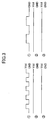
- Fig. 3 is a timing chart showing the driving operations of various driving circuits shown in Fig. 2.
- the waveforms shown on the left side represent voltages applied to the upper ITO layers, while the waveforms shown on the right side represent voltages applied to the lower ITO layers, representing the waveforms of driving voltages of the picto-display drive 2, the guard electrode drive 6 and the liquid crystal drive 3.
- 1 ⁇ represents the waveforms of the driving voltages of the picto-display drive 2
- 2 ⁇ represents the waveforms of the driving voltages of the guard electrode drive 6
- 3 ⁇ represents the waveforms of the driving voltages of the liquid crystal drive 3.
- the picto-display area A can display by virtue of a voltage applied between the upper and lower ITO layers 12 and 13.
- the upper ITO layer 12 is made ON and OFF repeatedly in a predetermined period, while the lower ITO layer 13 is also made ON and OFF repeatedly in a predetermined period which is 1/2 of the upper ITO layer 12, thereby maintaining an average voltage of 1.5 V.
- the dot-display area C can display by virtue of a voltage applied between the upper and lower ITO layers 14 and 15.
- the dot-display area C is driven by a power-saving mode so that it is in a non-display state, the upper and lower ITO layers 14 and 15 are placed at the same potential so that a voltage therebetween becomes zero.
- a driving voltage (Vdd) of 3. 1 V is needed to be applied between the upper and lower ITO layers 14 and 15 in order to maintain a driving function.
- the picto-display area A is driven by an average effective voltage 1.5 V so as to be maintained in a display state
- the dot-display area C is driven by a power-saving mode so as to stop its display and is fixed at a DC voltage of 3.1 V, resulting in a voltage difference between the picto-display area A and the dot-display area C and hence resulting a mutual interference between the two display areas.
- the guard electrode section B is eliminated when the dot-display area C is at a voltage Vdd, guard electrode section B is also set at a voltage which is equal to Vdd.
- guard electrode section B When dot-display area C is at a voltage GND, guard electrode section B is also set at a voltage which is equal to GND.
- the dot-display area C driven by the liquid crystal drive 3 when in its non-display state, receives a voltage supply which is either a voltage VDD or a voltage GND, depending upon the type of the liquid crystal drive 3.
- a voltage Vdd is applied to effect a non-display state.
- Fig. 4 is an explanatory view showing a difference between an example of the present invention and that of a prior art.
- the same elements as those shown in Fig. 1 are represented by the same reference numerals.
- (a) is a front view of the liquid crystal panel
- (b) is a sectional view of the liquid crystal panel, showing the movement of the ionic substances during a power-saving mode, according a prior art
- (c) is a sectional view of the liquid crystal panel, showing the movement of the ionic substances during a power-saving mode, according to the present invention.
- the present invention has been accomplished by providing the guard electrode section B between picto-display area A and the dot-display area C. Therefore, as shown in (c) of Fig. 3, when the picto-display area A is driven by an average effective voltage 1.5 V while the dot-display area C is in its non-display state, since the voltage applied on the guard electrode section B is 3.1 V which is the same voltage as applied to the dot-display area C, the movement of the ionic substances can be effectively stopped by the guard electrode section B, thereby preventing the ionic substances from invading into the dot-display area C.
- the liquid crystal panel 1 comprises a plurality of liquid crystal display areas (picto-display area A and the dot-display area C) which are controlled and driven by different driving manners (different driving voltages), an electrode section B is disposed between the plurality of liquid crystal display areas, a driving voltage for driving the electrode section B is equal to at least one of the different driving voltages for driving the plurality of different liquid crystal display areas. Therefore, it is sure to prevent an undesired mutual interference between the plurality of liquid crystal display areas, thereby preventing the dot-display area C from becoming darkened and preventing the picto-display area A from becoming nicked, thereby improving the display quality of the liquid crystal panel.
- the voltage applied in the guard electrode section B is set to be equal to the voltage applied to the dot-display area C
- the voltage applied in the guard electrode section B is set to be equal to the voltage applied to the picto-display area A, depending upon whether the ionicity of liquid crystal used in the liquid crystal panel is high or not.
- a voltage Vdd (3.1 V) is applied between the upper and lower ITO layers of the dot-display area C to keep it at a non-display state
- the dot-display area C connected to GND to keep it at a non-display state.
- electrode section B is disposed between the plurality of liquid crystal display areas, and since a driving voltage for driving the electrode section B is equal to at least one of the different driving voltages for driving the plurality of different liquid crystal display areas, it is sure to prevent an undesired movement of ionic substances from one display area to another, thus preventing mutual interference between the plurality of liquid crystal display areas, thereby preventing any of the display areas from becoming darkened or nicked, thus improving the display quality of the liquid crystal panel.
Landscapes
- Engineering & Computer Science (AREA)
- Chemical & Material Sciences (AREA)
- Crystallography & Structural Chemistry (AREA)
- Physics & Mathematics (AREA)
- Computer Hardware Design (AREA)
- General Physics & Mathematics (AREA)
- Theoretical Computer Science (AREA)
- Liquid Crystal (AREA)
- Liquid Crystal Display Device Control (AREA)
- Control Of Indicators Other Than Cathode Ray Tubes (AREA)
- Devices For Indicating Variable Information By Combining Individual Elements (AREA)
Abstract
Description
Claims (7)
- A liquid crystal panel (1) comprising:a pair of light transmissible substrate plates;a plurality of liquid crystal display areas controlled and driven by different driving manners; andan electrode section (B) disposed between the plurality of liquid crystal display areas.
- A liquid crystal panel (1) according to claim 1, wherein said different driving manners are different driving voltages.
- A liquid crystal panel (1) according to claim 1, wherein the plurality of liquid crystal display areas include at least one static-display area and at least one dot-display area (C) .
- A liquid crystal panel (1) according to claim 1 , 2 or 3, wherein the plurality of liquid crystal display areas include at least one constantly displayed area, and at least one area capable of independently changing-over between a displayed state and a non-displayed state.
- A liquid crystal panel (1) according to claim 4, wherein the non-displayed state is a state controlled by a power-saving mode.
- A liquid crystal panel (1) according to claim 1, wherein a driving voltage for driving the electrode section (B) is equal to at least one of the different driving voltages for driving the plurality of different liquid crystal display areas.
- A liquid crystal panel (1) according to claim 6, wherein the driving voltage for driving the electrode section (B) is selected in view of the property of a liquid crystal used in the liquid crystal panel (1) .
Applications Claiming Priority (2)
| Application Number | Priority Date | Filing Date | Title |
|---|---|---|---|
| JP29804699A JP2001117110A (en) | 1999-10-20 | 1999-10-20 | Liquid crystal panel |
| JP29804699 | 1999-10-20 |
Publications (3)
| Publication Number | Publication Date |
|---|---|
| EP1094439A2 true EP1094439A2 (en) | 2001-04-25 |
| EP1094439A3 EP1094439A3 (en) | 2002-04-17 |
| EP1094439B1 EP1094439B1 (en) | 2004-01-02 |
Family
ID=17854439
Family Applications (1)
| Application Number | Title | Priority Date | Filing Date |
|---|---|---|---|
| EP00122877A Expired - Lifetime EP1094439B1 (en) | 1999-10-20 | 2000-10-20 | Liquid crystal panel |
Country Status (4)
| Country | Link |
|---|---|
| US (1) | US6657681B1 (en) |
| EP (1) | EP1094439B1 (en) |
| JP (1) | JP2001117110A (en) |
| DE (1) | DE60007497T2 (en) |
Cited By (1)
| Publication number | Priority date | Publication date | Assignee | Title |
|---|---|---|---|---|
| EP2043067A3 (en) * | 2007-09-10 | 2009-09-23 | GE Security, Inc. | Keypad for a security system |
Families Citing this family (6)
| Publication number | Priority date | Publication date | Assignee | Title |
|---|---|---|---|---|
| JP4698095B2 (en) * | 2001-09-25 | 2011-06-08 | 京セラ株式会社 | Liquid crystal display device and display device |
| JP2003140180A (en) * | 2001-11-02 | 2003-05-14 | Seiko Instruments Inc | Liquid crystal display |
| SE0400556D0 (en) * | 2004-03-05 | 2004-03-05 | Pricer Ab | Electronic shelf labeling system, electronic label, handheld device and method in an electronic labeling system |
| KR100659065B1 (en) * | 2004-10-12 | 2006-12-19 | 삼성에스디아이 주식회사 | Driving device of electroluminescent display panel to perform energy regeneration |
| DE102009031039B4 (en) * | 2009-06-30 | 2015-12-31 | GM Global Technology Operations LLC (n. d. Ges. d. Staates Delaware) | Liquid crystal display with several drive segments |
| CN109584717B (en) * | 2019-01-22 | 2021-03-09 | 上海天马有机发光显示技术有限公司 | Display panel and display device |
Family Cites Families (6)
| Publication number | Priority date | Publication date | Assignee | Title |
|---|---|---|---|---|
| JPS576882A (en) | 1980-06-16 | 1982-01-13 | Hitachi Ltd | Liquid crystal display element |
| GB2195195B (en) | 1986-09-20 | 1990-10-17 | Emi Plc Thorn | Display device |
| JPH05241138A (en) * | 1991-12-06 | 1993-09-21 | Canon Inc | Liquid crystal optical element |
| CN1106000C (en) * | 1994-12-01 | 2003-04-16 | 皇家菲利浦电子有限公司 | Display unit with dummy electrode |
| JPH09146499A (en) | 1995-11-22 | 1997-06-06 | Toshiba Corp | Information equipment |
| JPH11281961A (en) * | 1998-03-31 | 1999-10-15 | Optrex Corp | Driving method for color liquid crystal display element |
-
1999
- 1999-10-20 JP JP29804699A patent/JP2001117110A/en not_active Withdrawn
-
2000
- 2000-10-16 US US09/688,210 patent/US6657681B1/en not_active Expired - Fee Related
- 2000-10-20 DE DE60007497T patent/DE60007497T2/en not_active Expired - Fee Related
- 2000-10-20 EP EP00122877A patent/EP1094439B1/en not_active Expired - Lifetime
Cited By (2)
| Publication number | Priority date | Publication date | Assignee | Title |
|---|---|---|---|---|
| EP2043067A3 (en) * | 2007-09-10 | 2009-09-23 | GE Security, Inc. | Keypad for a security system |
| US8059095B2 (en) | 2007-09-10 | 2011-11-15 | Utc Fire & Security Americas Corporation, Inc. | Keypad for a security system |
Also Published As
| Publication number | Publication date |
|---|---|
| EP1094439A3 (en) | 2002-04-17 |
| EP1094439B1 (en) | 2004-01-02 |
| DE60007497T2 (en) | 2004-12-02 |
| US6657681B1 (en) | 2003-12-02 |
| JP2001117110A (en) | 2001-04-27 |
| DE60007497D1 (en) | 2004-02-05 |
Similar Documents
| Publication | Publication Date | Title |
|---|---|---|
| US5828367A (en) | Display arrangement | |
| JP3862994B2 (en) | Display device driving method and display device using the same | |
| WO2005020199A3 (en) | Methods for controlling electro-optic displays | |
| US11615759B2 (en) | Pixel circuit, display module and driving method thereof | |
| KR100852036B1 (en) | Liquid crystal display element driving method and liquid crystal display using the same | |
| KR100599756B1 (en) | LCD and its driving method | |
| EP2053588B1 (en) | Display device and display method | |
| US7190340B2 (en) | Liquid crystal display | |
| US20110292021A1 (en) | Liquid crystal display device and method of driving same | |
| EP1094439B1 (en) | Liquid crystal panel | |
| CN103631552B (en) | Method and device for realizing energy conservation and fine control of display module | |
| KR100475115B1 (en) | Liquid crystal display device | |
| JP2007058158A (en) | Electro-optical device, method of driving electro-optical device, and electronic apparatus | |
| US20070024564A1 (en) | Electro-optical device, method of driving electro-optical device, and electronic apparatus | |
| KR100499578B1 (en) | driving circuit of liquid crystal display device | |
| JP4623429B2 (en) | Electrophoretic display device, electronic apparatus, driving method of electrophoretic display device, and controller | |
| KR100531478B1 (en) | Liquid crystal display panel and method of dirving the same | |
| KR100487437B1 (en) | Method for driving normal mode in a wide mode liquid crystal display device | |
| JP2005266573A (en) | Electro-optical device, control device for electro-optical device, control method for electro-optical device, and electronic apparatus | |
| JP2003295840A (en) | Liquid crystal display device and drive control method thereof | |
| US7091965B2 (en) | Display device, method of driving the same, and electronic equipment | |
| US20060145988A1 (en) | Active matrix liquid crystal display | |
| EP1170622A1 (en) | Display and method for driving the same | |
| JP2014174215A (en) | Planar display device and driving method thereof | |
| KR100504544B1 (en) | driving circuit of liquid crystal display device |
Legal Events
| Date | Code | Title | Description |
|---|---|---|---|
| PUAI | Public reference made under article 153(3) epc to a published international application that has entered the european phase |
Free format text: ORIGINAL CODE: 0009012 |
|
| AK | Designated contracting states |
Kind code of ref document: A2 Designated state(s): DE FR GB Kind code of ref document: A2 Designated state(s): AT BE CH CY DE DK ES FI FR GB GR IE IT LI LU MC NL PT SE |
|
| AX | Request for extension of the european patent |
Free format text: AL;LT;LV;MK;RO;SI |
|
| PUAL | Search report despatched |
Free format text: ORIGINAL CODE: 0009013 |
|
| AK | Designated contracting states |
Kind code of ref document: A3 Designated state(s): AT BE CH CY DE DK ES FI FR GB GR IE IT LI LU MC NL PT SE |
|
| AX | Request for extension of the european patent |
Free format text: AL;LT;LV;MK;RO;SI |
|
| 17P | Request for examination filed |
Effective date: 20020417 |
|
| 17Q | First examination report despatched |
Effective date: 20020718 |
|
| AKX | Designation fees paid |
Free format text: DE FR GB |
|
| GRAH | Despatch of communication of intention to grant a patent |
Free format text: ORIGINAL CODE: EPIDOS IGRA |
|
| GRAS | Grant fee paid |
Free format text: ORIGINAL CODE: EPIDOSNIGR3 |
|
| GRAA | (expected) grant |
Free format text: ORIGINAL CODE: 0009210 |
|
| AK | Designated contracting states |
Kind code of ref document: B1 Designated state(s): DE FR GB |
|
| REG | Reference to a national code |
Ref country code: GB Ref legal event code: FG4D |
|
| REG | Reference to a national code |
Ref country code: IE Ref legal event code: FG4D |
|
| REF | Corresponds to: |
Ref document number: 60007497 Country of ref document: DE Date of ref document: 20040205 Kind code of ref document: P |
|
| ET | Fr: translation filed | ||
| REG | Reference to a national code |
Ref country code: GB Ref legal event code: 746 Effective date: 20041004 |
|
| PLBE | No opposition filed within time limit |
Free format text: ORIGINAL CODE: 0009261 |
|
| STAA | Information on the status of an ep patent application or granted ep patent |
Free format text: STATUS: NO OPPOSITION FILED WITHIN TIME LIMIT |
|
| REG | Reference to a national code |
Ref country code: FR Ref legal event code: D6 |
|
| 26N | No opposition filed |
Effective date: 20041005 |
|
| PGFP | Annual fee paid to national office [announced via postgrant information from national office to epo] |
Ref country code: GB Payment date: 20051006 Year of fee payment: 6 |
|
| PGFP | Annual fee paid to national office [announced via postgrant information from national office to epo] |
Ref country code: FR Payment date: 20051019 Year of fee payment: 6 |
|
| PGFP | Annual fee paid to national office [announced via postgrant information from national office to epo] |
Ref country code: DE Payment date: 20061228 Year of fee payment: 7 |
|
| GBPC | Gb: european patent ceased through non-payment of renewal fee |
Effective date: 20061020 |
|
| REG | Reference to a national code |
Ref country code: FR Ref legal event code: ST Effective date: 20070629 |
|
| PG25 | Lapsed in a contracting state [announced via postgrant information from national office to epo] |
Ref country code: GB Free format text: LAPSE BECAUSE OF NON-PAYMENT OF DUE FEES Effective date: 20061020 |
|
| PG25 | Lapsed in a contracting state [announced via postgrant information from national office to epo] |
Ref country code: FR Free format text: LAPSE BECAUSE OF NON-PAYMENT OF DUE FEES Effective date: 20061031 |
|
| PG25 | Lapsed in a contracting state [announced via postgrant information from national office to epo] |
Ref country code: DE Free format text: LAPSE BECAUSE OF NON-PAYMENT OF DUE FEES Effective date: 20080501 |