EP1094130A3 - Method and apparatus for plasma processing of surfaces - Google Patents
Method and apparatus for plasma processing of surfaces Download PDFInfo
- Publication number
- EP1094130A3 EP1094130A3 EP00117039A EP00117039A EP1094130A3 EP 1094130 A3 EP1094130 A3 EP 1094130A3 EP 00117039 A EP00117039 A EP 00117039A EP 00117039 A EP00117039 A EP 00117039A EP 1094130 A3 EP1094130 A3 EP 1094130A3
- Authority
- EP
- European Patent Office
- Prior art keywords
- workpiece
- plasma
- electrons
- electric field
- generated
- Prior art date
- Legal status (The legal status is an assumption and is not a legal conclusion. Google has not performed a legal analysis and makes no representation as to the accuracy of the status listed.)
- Withdrawn
Links
Classifications
-
- H—ELECTRICITY
- H01—ELECTRIC ELEMENTS
- H01J—ELECTRIC DISCHARGE TUBES OR DISCHARGE LAMPS
- H01J37/00—Discharge tubes with provision for introducing objects or material to be exposed to the discharge, e.g. for the purpose of examination or processing thereof
- H01J37/32—Gas-filled discharge tubes
- H01J37/32009—Arrangements for generation of plasma specially adapted for examination or treatment of objects, e.g. plasma sources
-
- C—CHEMISTRY; METALLURGY
- C23—COATING METALLIC MATERIAL; COATING MATERIAL WITH METALLIC MATERIAL; CHEMICAL SURFACE TREATMENT; DIFFUSION TREATMENT OF METALLIC MATERIAL; COATING BY VACUUM EVAPORATION, BY SPUTTERING, BY ION IMPLANTATION OR BY CHEMICAL VAPOUR DEPOSITION, IN GENERAL; INHIBITING CORROSION OF METALLIC MATERIAL OR INCRUSTATION IN GENERAL
- C23C—COATING METALLIC MATERIAL; COATING MATERIAL WITH METALLIC MATERIAL; SURFACE TREATMENT OF METALLIC MATERIAL BY DIFFUSION INTO THE SURFACE, BY CHEMICAL CONVERSION OR SUBSTITUTION; COATING BY VACUUM EVAPORATION, BY SPUTTERING, BY ION IMPLANTATION OR BY CHEMICAL VAPOUR DEPOSITION, IN GENERAL
- C23C14/00—Coating by vacuum evaporation, by sputtering or by ion implantation of the coating forming material
- C23C14/22—Coating by vacuum evaporation, by sputtering or by ion implantation of the coating forming material characterised by the process of coating
- C23C14/24—Vacuum evaporation
- C23C14/32—Vacuum evaporation by explosion; by evaporation and subsequent ionisation of the vapours, e.g. ion-plating
-
- C—CHEMISTRY; METALLURGY
- C23—COATING METALLIC MATERIAL; COATING MATERIAL WITH METALLIC MATERIAL; CHEMICAL SURFACE TREATMENT; DIFFUSION TREATMENT OF METALLIC MATERIAL; COATING BY VACUUM EVAPORATION, BY SPUTTERING, BY ION IMPLANTATION OR BY CHEMICAL VAPOUR DEPOSITION, IN GENERAL; INHIBITING CORROSION OF METALLIC MATERIAL OR INCRUSTATION IN GENERAL
- C23C—COATING METALLIC MATERIAL; COATING MATERIAL WITH METALLIC MATERIAL; SURFACE TREATMENT OF METALLIC MATERIAL BY DIFFUSION INTO THE SURFACE, BY CHEMICAL CONVERSION OR SUBSTITUTION; COATING BY VACUUM EVAPORATION, BY SPUTTERING, BY ION IMPLANTATION OR BY CHEMICAL VAPOUR DEPOSITION, IN GENERAL
- C23C16/00—Chemical coating by decomposition of gaseous compounds, without leaving reaction products of surface material in the coating, i.e. chemical vapour deposition [CVD] processes
- C23C16/44—Chemical coating by decomposition of gaseous compounds, without leaving reaction products of surface material in the coating, i.e. chemical vapour deposition [CVD] processes characterised by the method of coating
- C23C16/50—Chemical coating by decomposition of gaseous compounds, without leaving reaction products of surface material in the coating, i.e. chemical vapour deposition [CVD] processes characterised by the method of coating using electric discharges
- C23C16/505—Chemical coating by decomposition of gaseous compounds, without leaving reaction products of surface material in the coating, i.e. chemical vapour deposition [CVD] processes characterised by the method of coating using electric discharges using radio frequency discharges
- C23C16/509—Chemical coating by decomposition of gaseous compounds, without leaving reaction products of surface material in the coating, i.e. chemical vapour deposition [CVD] processes characterised by the method of coating using electric discharges using radio frequency discharges using internal electrodes
-
- C—CHEMISTRY; METALLURGY
- C23—COATING METALLIC MATERIAL; COATING MATERIAL WITH METALLIC MATERIAL; CHEMICAL SURFACE TREATMENT; DIFFUSION TREATMENT OF METALLIC MATERIAL; COATING BY VACUUM EVAPORATION, BY SPUTTERING, BY ION IMPLANTATION OR BY CHEMICAL VAPOUR DEPOSITION, IN GENERAL; INHIBITING CORROSION OF METALLIC MATERIAL OR INCRUSTATION IN GENERAL
- C23C—COATING METALLIC MATERIAL; COATING MATERIAL WITH METALLIC MATERIAL; SURFACE TREATMENT OF METALLIC MATERIAL BY DIFFUSION INTO THE SURFACE, BY CHEMICAL CONVERSION OR SUBSTITUTION; COATING BY VACUUM EVAPORATION, BY SPUTTERING, BY ION IMPLANTATION OR BY CHEMICAL VAPOUR DEPOSITION, IN GENERAL
- C23C16/00—Chemical coating by decomposition of gaseous compounds, without leaving reaction products of surface material in the coating, i.e. chemical vapour deposition [CVD] processes
- C23C16/44—Chemical coating by decomposition of gaseous compounds, without leaving reaction products of surface material in the coating, i.e. chemical vapour deposition [CVD] processes characterised by the method of coating
- C23C16/50—Chemical coating by decomposition of gaseous compounds, without leaving reaction products of surface material in the coating, i.e. chemical vapour deposition [CVD] processes characterised by the method of coating using electric discharges
- C23C16/517—Chemical coating by decomposition of gaseous compounds, without leaving reaction products of surface material in the coating, i.e. chemical vapour deposition [CVD] processes characterised by the method of coating using electric discharges using a combination of discharges covered by two or more of groups C23C16/503 - C23C16/515
Landscapes
- Chemical & Material Sciences (AREA)
- Engineering & Computer Science (AREA)
- Organic Chemistry (AREA)
- Plasma & Fusion (AREA)
- Physics & Mathematics (AREA)
- Chemical Kinetics & Catalysis (AREA)
- Materials Engineering (AREA)
- Mechanical Engineering (AREA)
- Metallurgy (AREA)
- General Chemical & Material Sciences (AREA)
- Analytical Chemistry (AREA)
- Chemical Vapour Deposition (AREA)
- Physical Vapour Deposition (AREA)
- Plasma Technology (AREA)
- Physical Or Chemical Processes And Apparatus (AREA)
- Treatments Of Macromolecular Shaped Articles (AREA)
Abstract
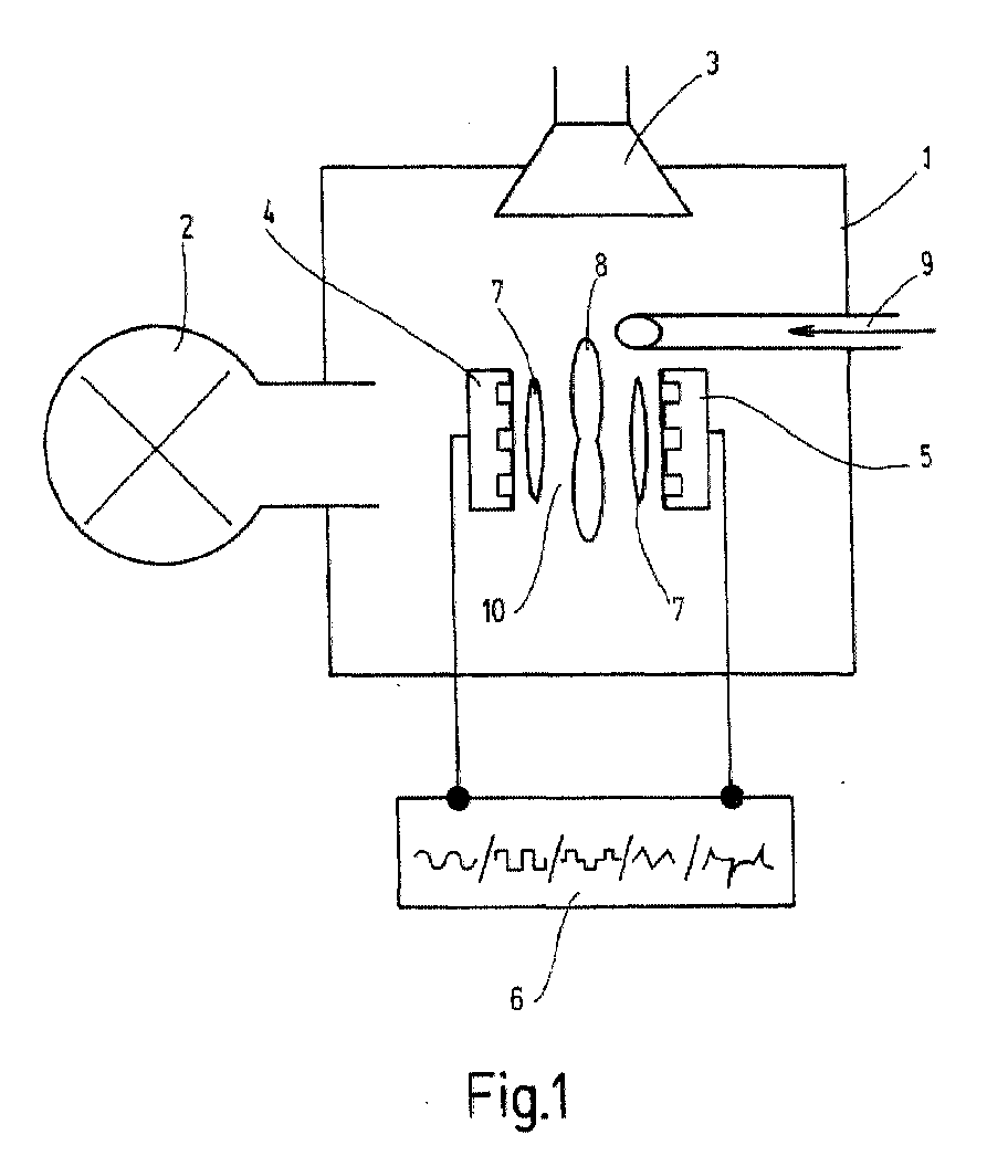
Bei einem Verfahren zum Behandeln und Beschichten
einer Oberfläche eines Werkstücks (8) mit einem
Plasma, bei dem ein alternierendes elektrisches
Feld zwischen dem Werkstück (8) und einer ersten
Plasmaelektrode (4) erzeugt wird, um aus der Richtung
des zugeordneten Plasmas (7) abwechselnd Ionen
und Elektronen auf die Oberfläche zu lenken, ist
vorgesehen, daß das Werkstück den Ionen und Elektronen
in einem Zwischenraum zwischen der ersten
und wenigstens einer weiteren Plasmaelektrode (5)
ausgesetzt wird, und daß zwischen jeder der weiteren
Plasmaelektroden (5) und dem Werkstück (8)
ebenfalls ein alternierendes elektrisches Feld erzeugt
wird, und die alternierenden Felder aller
Plasmaelektroden (4,5) jeweils in einem festen Phasenverhältnis
zueinander stehen. Auf diese Weise
bilden sich auf jeder Oberfläche des Werkstücks zyklisch
sowohl negative wie positive Potentiale.
Diese führen abwechselnd zum positiven Ionenbombardement
der Oberfläche und zu Neutralisation durch
Elektronen der dadurch entstehenden Oberflächenladung.
Applications Claiming Priority (2)
| Application Number | Priority Date | Filing Date | Title |
|---|---|---|---|
| DE1999151017 DE19951017A1 (en) | 1999-10-22 | 1999-10-22 | Method and device for plasma treatment of surfaces |
| DE19951017 | 1999-10-22 |
Publications (2)
| Publication Number | Publication Date |
|---|---|
| EP1094130A2 EP1094130A2 (en) | 2001-04-25 |
| EP1094130A3 true EP1094130A3 (en) | 2002-08-14 |
Family
ID=7926588
Family Applications (1)
| Application Number | Title | Priority Date | Filing Date |
|---|---|---|---|
| EP00117039A Withdrawn EP1094130A3 (en) | 1999-10-22 | 2000-08-09 | Method and apparatus for plasma processing of surfaces |
Country Status (3)
| Country | Link |
|---|---|
| EP (1) | EP1094130A3 (en) |
| JP (1) | JP2001190948A (en) |
| DE (1) | DE19951017A1 (en) |
Families Citing this family (15)
| Publication number | Priority date | Publication date | Assignee | Title |
|---|---|---|---|---|
| JP2003055772A (en) * | 2001-08-10 | 2003-02-26 | Shinku Device:Kk | Ac discharge plasma cvd film deposition apparatus |
| US7342361B2 (en) | 2005-05-11 | 2008-03-11 | Dublin City University | Plasma source |
| IES20050301A2 (en) | 2005-05-11 | 2006-11-15 | Univ Dublin City | Plasma source |
| JP4525929B2 (en) * | 2006-02-28 | 2010-08-18 | ノーリツ鋼機株式会社 | Work processing device |
| JP4930983B2 (en) * | 2006-06-30 | 2012-05-16 | 国立大学法人名古屋大学 | Atmospheric pressure plasma generator |
| JP4984285B2 (en) * | 2007-01-23 | 2012-07-25 | 独立行政法人産業技術総合研究所 | High density plasma processing equipment |
| JP4296523B2 (en) | 2007-09-28 | 2009-07-15 | 勝 堀 | Plasma generator |
| JP5145076B2 (en) * | 2008-02-22 | 2013-02-13 | Nuエコ・エンジニアリング株式会社 | Plasma generator |
| DE102008028537B4 (en) * | 2008-06-16 | 2012-11-29 | Fraunhofer-Gesellschaft zur Förderung der angewandten Forschung e.V. | Method for depositing a scratch-resistant coating on a plastic substrate |
| DE102008028542B4 (en) * | 2008-06-16 | 2012-07-12 | Fraunhofer-Gesellschaft zur Förderung der angewandten Forschung e.V. | Method and apparatus for depositing a layer on a substrate by means of a plasma-enhanced chemical reaction |
| DE102008056968B4 (en) * | 2008-11-13 | 2011-01-05 | Fraunhofer-Gesellschaft zur Förderung der angewandten Forschung e.V. | A method of depositing a nanocomposite layer on a substrate by chemical vapor deposition |
| US9443703B2 (en) | 2011-12-19 | 2016-09-13 | Fraunhofer-Gesellschaft zur Förderung der angewandten Forschung e.V. | Apparatus for generating a hollow cathode arc discharge plasma |
| DE102012024340A1 (en) * | 2012-12-13 | 2014-06-18 | Oerlikon Trading Ag, Trübbach | plasma source |
| CN103606508A (en) * | 2013-11-27 | 2014-02-26 | 苏州市奥普斯等离子体科技有限公司 | Processing device for granular material surface plasma |
| CN111593321A (en) * | 2018-01-23 | 2020-08-28 | 温州职业技术学院 | Method for depositing DLC coating by twinning load medium-frequency alternating current PECVD |
Citations (8)
| Publication number | Priority date | Publication date | Assignee | Title |
|---|---|---|---|---|
| DE3802852A1 (en) * | 1988-02-01 | 1989-08-03 | Leybold Ag | Device for coating a substrate with a material obtained from a plasma |
| JPH02102038A (en) * | 1988-10-12 | 1990-04-13 | Furukawa Alum Co Ltd | Corrosion resistant metal plate |
| US5162633A (en) * | 1988-06-29 | 1992-11-10 | Hitachi, Ltd. | Microwave-excited plasma processing apparatus |
| US5227202A (en) * | 1989-09-22 | 1993-07-13 | Balzers Aktiengesellschaft | Method for chemical coating on opposite surfaces of workpieces |
| US5440206A (en) * | 1992-06-26 | 1995-08-08 | Tokyo Electron Ltd. | Plasma processing apparatus comprising means for generating rotating magnetic field |
| JPH0945496A (en) * | 1995-08-03 | 1997-02-14 | Hitachi Ltd | Ecr plasma processing device |
| US5789040A (en) * | 1997-05-21 | 1998-08-04 | Optical Coating Laboratory, Inc. | Methods and apparatus for simultaneous multi-sided coating of optical thin film designs using dual-frequency plasma-enhanced chemical vapor deposition |
| JPH1129873A (en) * | 1997-07-11 | 1999-02-02 | Sekisui Chem Co Ltd | Formation of laminated film and forming device therefor |
Family Cites Families (2)
| Publication number | Priority date | Publication date | Assignee | Title |
|---|---|---|---|---|
| DE4034034A1 (en) * | 1990-10-26 | 1992-05-14 | Leybold Ag | Coating weakly corrosion resistant substrate - useful in making decorative layers, without applying galvanic protection and is effective and simple |
| DE19651615C1 (en) * | 1996-12-12 | 1997-07-10 | Fraunhofer Ges Forschung | Sputter coating to produce carbon layer for e.g. magnetic heads |
-
1999
- 1999-10-22 DE DE1999151017 patent/DE19951017A1/en not_active Ceased
-
2000
- 2000-08-09 EP EP00117039A patent/EP1094130A3/en not_active Withdrawn
- 2000-10-20 JP JP2000321399A patent/JP2001190948A/en active Pending
Patent Citations (8)
| Publication number | Priority date | Publication date | Assignee | Title |
|---|---|---|---|---|
| DE3802852A1 (en) * | 1988-02-01 | 1989-08-03 | Leybold Ag | Device for coating a substrate with a material obtained from a plasma |
| US5162633A (en) * | 1988-06-29 | 1992-11-10 | Hitachi, Ltd. | Microwave-excited plasma processing apparatus |
| JPH02102038A (en) * | 1988-10-12 | 1990-04-13 | Furukawa Alum Co Ltd | Corrosion resistant metal plate |
| US5227202A (en) * | 1989-09-22 | 1993-07-13 | Balzers Aktiengesellschaft | Method for chemical coating on opposite surfaces of workpieces |
| US5440206A (en) * | 1992-06-26 | 1995-08-08 | Tokyo Electron Ltd. | Plasma processing apparatus comprising means for generating rotating magnetic field |
| JPH0945496A (en) * | 1995-08-03 | 1997-02-14 | Hitachi Ltd | Ecr plasma processing device |
| US5789040A (en) * | 1997-05-21 | 1998-08-04 | Optical Coating Laboratory, Inc. | Methods and apparatus for simultaneous multi-sided coating of optical thin film designs using dual-frequency plasma-enhanced chemical vapor deposition |
| JPH1129873A (en) * | 1997-07-11 | 1999-02-02 | Sekisui Chem Co Ltd | Formation of laminated film and forming device therefor |
Non-Patent Citations (3)
| Title |
|---|
| PATENT ABSTRACTS OF JAPAN vol. 014, no. 311 (M - 0994) 4 July 1990 (1990-07-04) * |
| PATENT ABSTRACTS OF JAPAN vol. 1997, no. 06 30 June 1997 (1997-06-30) * |
| PATENT ABSTRACTS OF JAPAN vol. 1999, no. 05 31 May 1999 (1999-05-31) * |
Also Published As
| Publication number | Publication date |
|---|---|
| DE19951017A1 (en) | 2001-05-03 |
| EP1094130A2 (en) | 2001-04-25 |
| JP2001190948A (en) | 2001-07-17 |
Similar Documents
| Publication | Publication Date | Title |
|---|---|---|
| EP1094130A3 (en) | Method and apparatus for plasma processing of surfaces | |
| DE3733135C1 (en) | Device for coating or etching using a plasma | |
| EP1902156B1 (en) | Method for treating plasma and/or covering plasma of workpieces under continuous atmospheric pressure | |
| EP0732727A3 (en) | Use and method for treatment of surfaces by means of a barrier discharge device producing plasma particles and/or UV-radiation | |
| DE3140237C2 (en) | Device for plasma etching a sample | |
| DE2248367C3 (en) | Device for keeping the chamber walls free of dye in a treatment chamber for electrostatic dye application | |
| DE69319869T2 (en) | Regulation of the surface potential in the plasma processing of materials | |
| CH625974A5 (en) | ||
| DE2646798C2 (en) | Device for the electrical charging of liquid or solid particles in a gas, especially air flow and application of the charged particles to surfaces | |
| DE3614384A1 (en) | Method for coating substrates in a vacuum chamber | |
| EP0349556A1 (en) | Process and device for the surface treatment of semiconductors by particle bombardment. | |
| DE1001448T1 (en) | Thin film plasma treatment device | |
| EP0782173A3 (en) | Apparatus for coating a substrate by means of a chemical vapour deposition process | |
| DE3217708A1 (en) | METHOD AND DEVICE FOR PRODUCING AMORPHOUS SILICON FILMS | |
| EP0966020A3 (en) | Method and apparatus for monitoring charge neutralization operation | |
| WO1997034024A1 (en) | Means for vacuum coating of bulk material | |
| DE2419265A1 (en) | DUST CHARGER FOR AN ELECTRIC DUST COLLECTOR | |
| US20090188803A1 (en) | Method and Device for Processing at Least Two Workpieces by Means of Electrochemical Treatment | |
| EP0390004A3 (en) | Method and device for the microwave-plasma etching | |
| WO2004032175A1 (en) | Device for the treatment of a web-type material in a plasma-assisted process | |
| EP0786793A2 (en) | Workpiece surface treatment device | |
| DE102016116762A1 (en) | Method for depositing a layer by means of a magnetron sputtering device | |
| EP0257620A2 (en) | Method and device for forming a layer by a chemical plasma process | |
| DE3609698A1 (en) | Device and method for ionisation or neutralisation of a gas flow and the particles contained in it | |
| DE2228424B2 (en) | Process for producing a lithographic surface on an aluminum strip by electrolysis |
Legal Events
| Date | Code | Title | Description |
|---|---|---|---|
| PUAI | Public reference made under article 153(3) epc to a published international application that has entered the european phase |
Free format text: ORIGINAL CODE: 0009012 |
|
| AK | Designated contracting states |
Kind code of ref document: A2 Designated state(s): AT BE CH CY DE DK ES FI FR GB GR IE IT LI LU MC NL PT SE |
|
| AX | Request for extension of the european patent |
Free format text: AL;LT;LV;MK;RO;SI |
|
| PUAL | Search report despatched |
Free format text: ORIGINAL CODE: 0009013 |
|
| RIC1 | Information provided on ipc code assigned before grant |
Free format text: 7C 23C 16/503 A, 7C 23C 16/517 B, 7C 23C 16/458 B, 7C 23C 14/02 B, 7C 23C 14/35 B, 7H 01J 37/34 B, 7H 01J 37/32 B, 7C 23C 16/22 B |
|
| AK | Designated contracting states |
Kind code of ref document: A3 Designated state(s): AT BE CH CY DE DK ES FI FR GB GR IE IT LI LU MC NL PT SE |
|
| AX | Request for extension of the european patent |
Free format text: AL;LT;LV;MK;RO;SI |
|
| 17P | Request for examination filed |
Effective date: 20030214 |
|
| 17Q | First examination report despatched |
Effective date: 20030325 |
|
| AKX | Designation fees paid |
Designated state(s): AT BE CH CY DE DK ES FI FR GB GR IE IT LI LU MC NL PT SE |
|
| STAA | Information on the status of an ep patent application or granted ep patent |
Free format text: STATUS: THE APPLICATION IS DEEMED TO BE WITHDRAWN |
|
| 18D | Application deemed to be withdrawn |
Effective date: 20031014 |