EP1093703B1 - A method of manufacturing a transducer having a diaphragm with a predetermined tension - Google Patents
A method of manufacturing a transducer having a diaphragm with a predetermined tension Download PDFInfo
- Publication number
- EP1093703B1 EP1093703B1 EP99924802A EP99924802A EP1093703B1 EP 1093703 B1 EP1093703 B1 EP 1093703B1 EP 99924802 A EP99924802 A EP 99924802A EP 99924802 A EP99924802 A EP 99924802A EP 1093703 B1 EP1093703 B1 EP 1093703B1
- Authority
- EP
- European Patent Office
- Prior art keywords
- diaphragm
- tension
- stress
- thickness
- substrate
- Prior art date
- Legal status (The legal status is an assumption and is not a legal conclusion. Google has not performed a legal analysis and makes no representation as to the accuracy of the status listed.)
- Expired - Lifetime
Links
Images
Classifications
-
- H—ELECTRICITY
- H04—ELECTRIC COMMUNICATION TECHNIQUE
- H04R—LOUDSPEAKERS, MICROPHONES, GRAMOPHONE PICK-UPS OR LIKE ACOUSTIC ELECTROMECHANICAL TRANSDUCERS; DEAF-AID SETS; PUBLIC ADDRESS SYSTEMS
- H04R31/00—Apparatus or processes specially adapted for the manufacture of transducers or diaphragms therefor
- H04R31/003—Apparatus or processes specially adapted for the manufacture of transducers or diaphragms therefor for diaphragms or their outer suspension
-
- Y—GENERAL TAGGING OF NEW TECHNOLOGICAL DEVELOPMENTS; GENERAL TAGGING OF CROSS-SECTIONAL TECHNOLOGIES SPANNING OVER SEVERAL SECTIONS OF THE IPC; TECHNICAL SUBJECTS COVERED BY FORMER USPC CROSS-REFERENCE ART COLLECTIONS [XRACs] AND DIGESTS
- Y10—TECHNICAL SUBJECTS COVERED BY FORMER USPC
- Y10T—TECHNICAL SUBJECTS COVERED BY FORMER US CLASSIFICATION
- Y10T29/00—Metal working
- Y10T29/43—Electric condenser making
-
- Y—GENERAL TAGGING OF NEW TECHNOLOGICAL DEVELOPMENTS; GENERAL TAGGING OF CROSS-SECTIONAL TECHNOLOGIES SPANNING OVER SEVERAL SECTIONS OF THE IPC; TECHNICAL SUBJECTS COVERED BY FORMER USPC CROSS-REFERENCE ART COLLECTIONS [XRACs] AND DIGESTS
- Y10—TECHNICAL SUBJECTS COVERED BY FORMER USPC
- Y10T—TECHNICAL SUBJECTS COVERED BY FORMER US CLASSIFICATION
- Y10T29/00—Metal working
- Y10T29/49—Method of mechanical manufacture
- Y10T29/49002—Electrical device making
- Y10T29/49005—Acoustic transducer
-
- Y—GENERAL TAGGING OF NEW TECHNOLOGICAL DEVELOPMENTS; GENERAL TAGGING OF CROSS-SECTIONAL TECHNOLOGIES SPANNING OVER SEVERAL SECTIONS OF THE IPC; TECHNICAL SUBJECTS COVERED BY FORMER USPC CROSS-REFERENCE ART COLLECTIONS [XRACs] AND DIGESTS
- Y10—TECHNICAL SUBJECTS COVERED BY FORMER USPC
- Y10T—TECHNICAL SUBJECTS COVERED BY FORMER US CLASSIFICATION
- Y10T29/00—Metal working
- Y10T29/49—Method of mechanical manufacture
- Y10T29/49002—Electrical device making
- Y10T29/49007—Indicating transducer
Definitions
- This invention concerns a method of manufacturing a transducer having a diaphragm with a predetermined tension such as a microphone.
- Most microphones have a diaphragm which is caused to move by the sound pressure such as microphones with electrodynamic, piezoelectric, piezoresistive, or capacitive readout.
- the method of the invention applies to all such types of transducers having a diaphragm.
- a condenser microphone has as its basic components a diaphragm or membrane mounted in close proximity of a back plate.
- the diaphragm is retained along its periphery and can move or deflect in response to a sound pressure acting on a surface of the diaphragm.
- the diaphragm and the back plate form an electric capacitor, and when the diaphragm is deflected due to the sound pressure, the capacitance of the capacitor will vary.
- the capacitor will be charged with an electric charge corresponding to a DC voltage, and when the capacitance varies in response to the varying sound pressure, an electric AC voltage corresponding to the varying sound pressure will be superimposed on the DC voltage. This AC voltage is used as the output signal from the microphone.
- a diaphragm with a low tension is "soft" and will deflect more than a diaphragm with a high tension, resulting in a higher sensitivity, which is desirable.
- the diaphragm of a microphone of the type considered should therefore have a well defined low tension.
- Micromachined microphones have been developed by different research laboratories with applications such as in the telecommunication and hearing industry markets.
- One of the most challenging problems in the design and manufacturing of micromachined microphones is the controlled low tension of the diaphragm.
- Different sound detection principles have been suggested such as capacitive, piezoelectric, piezoresistive, optical, and tunneling read out. Most of which require a diaphragm with a tension below 50 N/m.
- battery-operated capacitive microphones with a low bias voltage of a few volts require very accurate control of the stress level in the diaphragm.
- a diaphragm is glued to a metal frame using weights at the rim of the frame to adjust the tension of the diaphragm. This technique is not applicable to micromachining technology.
- the tension of the diaphragm can be adjusted by developing new materials (e.g. silicon-rich silicon nitride), new deposition techniques (e.g. Plasma-Enhanced Chemical Vapor Deposition), new deposition conditions (e.g. by varying the temperature in a Low Pressure Chemical Vapor Deposition furnace), or subsequent temperature treatments (annealing treatments).
- new materials e.g. silicon-rich silicon nitride
- new deposition techniques e.g. Plasma-Enhanced Chemical Vapor Deposition
- new deposition conditions e.g. by varying the temperature in a Low Pressure Chemical Vapor Deposition furnace
- subsequent temperature treatments annealing treatments.
- the suspension of the diaphragm can relax tension e.g. through corrugations, hinges, springs, or in the most extreme case by suspending a plate.
- This invention proposes a new method which can be used to tune the diaphragm stress to a predetermined level during or after processing of a micromachined microphone.
- the diaphragm of the microphone resulting from the process of this invention is a sandwich of two or more layers (multi-layer, laminate, or composite) deposited on a rigid or stiff substrate.
- the diaphragm is formed by etching a hole into the substrate leaving the multi-layer as the diaphragm across the etched hole.
- the tension can be controlled much more accurately than by any other attempt to achieve a certain stress or tension level, because thickness can be controlled almost down to the atomic level in micro-technology. It allows to deposit layers in a stable regime, where the materials have little variations in their mechanical properties.
- the correct stress level is adjusted by choosing the correct mixture of materials rather than the correct materials properties.
- the total thickness of the diaphragm can be chosen independently of the stress/tension level.
- the total stress can be changed after deposition of the layers by changing the thickness of one or both of the outer layers. This can be done by known methods such as dry or wet etching to remove material from the outer layers, or by deposition/absorption of material to achieve thicker outer layers. Deposition on or etching of the outer layers will change the ratio of thickness. The stress or tension level of the composite diaphragm will thereby change.
- Etching processes can be wet etching processes using reactants such as HF, phosphoric acid, KOH, etc. or dry etching processes such as Reactive Ion Etching. Low etching rates can easily be achieved to support a controlled, accurate, and uniform removal of material. Deposition processes for tuning include physical and chemical vapor deposition.
- transducers according to the invention are very accurate and reproducible, and within one batch transducers can be manufactured with very small deviations between transducers in the same batch. This means that, with the claimed method, it is not necessary to measure the actual diaphragm tension on each individual transducer before adjusting the tension. It suffices to measure the actual diaphragm tension on selected transducers on selected wafers in the batch, and with sufficiently precise and predictable processes it is even not necessary to measure the actual diaphragm tension of transducers in every batch.
- the resulting diaphragms can be applied in many types of transducers such as condenser and other microphones, and specifically, in micromachined microphones based on semiconductor technology, in microphones in battery-operated equipment, sensitive microphones, and microphones with a high signal-to-noise ratio.
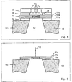
- the microphone in figure 1 has the following structure.
- a substrate 10 carries a diaphragm or membrane 11 by means of an intermediate spacer 12 between the substrate 10 and the diaphragm 11.
- a back plate 13 is situated with an intermediate spacer 14 between the back plate 13 and the diaphragm 11.
- the diaphragm 11 has three layers 11a, 11b and 11c.
- the substrate 10 consists of bulk crystalline silicon and the backplate 13 consists of polycrystalline silicon.
- the spacers 12 and 14 consist of an electrically insulating material, which in this case is silicon dioxide SiO 2 .
- the intermediate layer 11b consists of polycrystalline silicon, and the two outer layers 11a and 11c consist of silicon nitride.
- the diaphragm 11 is thin and its tension is low so that it is "soft" and movable about the shown position, where it is in equilibrium.
- the insulating spacer 14 provides an air gap 15 between the back plate 13 and the diaphragm 11, and the back plate 13 has a number of openings 16 giving access of sound to the air gap 15 and the diaphragm 11.
- a back chamber 17 On the opposite side of the diaphragm there is a back chamber 17, which is an opening in the substrate 10. If desired, the back chamber 17 can be connected to a further volume for acoustical purposes.
- the diaphragm 11 and the back plate 13 are both electrically conductive, and together they form an electrical capacitor. Sound entering through the openings 16 in the back plate 13 will reach the diaphragm 11 and will cause it to move in response to the sound pressure. Thereby the capacitance of the microphone will change correspondingly, since the air gap determines the capacitance.
- the capacitor formed by the diaphragm 11 and the back plate 13 is charged with an electrical charge corresponding to a DC voltage, and when the capacitance varies in response to the varying sound pressure, an electric AC voltage corresponding to the varying sound pressure will be superimposed on the DC voltage. This AC voltage is used as the output signal from the microphone.
- the process for manufacturing a microphone with the structure shown in figure 1 and described above involves mainly known technology.
- the polycrystalline silicon is itself a semiconductor but can if desired be made conducting by doping with suitable impurities such as boron (B) or phosphorus (P).
- suitable impurities such as boron (B) or phosphorus (P).
- the two outer layers 11a and 11c of the diaphragm consist of silicon nitride, which in combination with the B- or P-doped polycrystalline silicon in the intermediate layer of the diaphragm is particularly advantageous, as will be explained later.
- the intermediate layer 11b of the diaphragm consisting of B- or P- doped polycrystalline silicon has a compressive internal stress ⁇ ⁇ 0, whereas the two outer layers 11a and 11c consisting of silicon nitride both have a tensile internal stress ⁇ > 0, which need not be of the same size.
- the total or resulting tension of the diaphragm is the sum of the tension in the three layers 11a, 11b and 11c of the diaphragm.
- the stress is due to two factors. One factor is the technique used when depositing or building up the layer. This stress is called built-in stress. Another factor is the stress induced by a difference in thermal expansion coefficients of the different materials and is called thermal stress. Both stress contributions can be controlled, as will be explained in the following.
- the built-in stress can be relieved by the following method.
- the spacer material retaining the diaphragm consists of silicon dioxide which is a glassy material having a glass transition temperature.
- the spacer material will become viscous and loose its stiffness. Therefore, in this state the tension in the diaphragm will become completely relieved, since the viscous spacer material can not transfer any strain.
- the wafer is cooled.
- the spacer material will solidify and below the glass transition temperature the diaphragm will again become retained.
- the diaphragm will regain some tension, which is due to the material properties, which is referred to above as thermal stress.
- the thermal stress can be controlled by the following method. First, the actual tension and thickness of the diaphragm is measured and the actual stress calculated. The desired tension is achieved by calculating the necessary thickness adjustment considering the actual stress. There are several useable methods of measuring the actual tension of the diaphragm.
- One method of measuring the actual tension of the diaphragm is a test which involves pressurising the diaphragm of the microphone which causes the diaphragm to bulge, ie the diaphragm is given a unidirectional deflection. In practice this is done by pressurising a test diaphragm on the wafer.
- Figure 2 shows a beam of light 18, and preferably a laser beam which is directed onto the test diaphragm. This is done in the unpressurised state and also in the pressurised state, and the laser beam 18 will be reflected from the surface of the diaphragm.
- the bulging of the diaphragm caused by the pressurisation can e.g. be registered by an auto-focus system. When the deflection of the diaphragm and the air pressure causing the bulging are known, the actual tension of the diaphragm can be calculated.
- the diaphragm is excited thereby causing the diaphragm to oscillate.
- the excitation can be done either electrically or mechanically.
- the diaphragm will oscillate at its resonance frequency, which can be measured.
- the excitation signal can also be a sinusoidally oscillating force or voltage that is swept through the frequency range of interest for measuring the resonance frequency.
- the resonance frequency of the diaphragm is known, this can be used together with the other mechanical parameters of the diaphragm such as its dimensions and material to calculate the actual tension of the diaphragm.
- a third method for determining the tension uses test structures on the wafer which work as strain gauges.
- the actual tension and thickness of the diaphragm When the actual tension and thickness of the diaphragm is known the actual stress can be calculated. It can then be calculated how much the thickness of the diaphragm needs to be adjusted in order to obtain the desired tension.
- the microphone is preferably manufactured so that its diaphragm at this stage is too thick and therefore has a too high tension. From the above calculation of the desired thickness it is known how much material should be removed in a subsequent etching process that can be either dry or wet etching. As shown in figure 2A the layer 11a having a tensile stress is etched. This is done by etching slowly in a well controlled process, until precisely so much of the layer 11a as needed according to the calculation is removed by etching, and the diaphragm has obtained its predetermined tension.
- the diaphragm has a too low tension, extra material having tensile stress can be deposited by known methods to obtain the predetermined tension.
- the layer having a compressive stress can be etched in order to increase its tension.
- the tension of the diaphragm can by this method be shifted towards higher tension by etching a layer having relatively compressive stress or by depositing material having relatively tensile stress, and correspondingly, the tension of the diaphragm can be shifted towards lower tension by etching a layer having relatively tensile stress or by depositing material having relatively compressive stress.
Landscapes
- Engineering & Computer Science (AREA)
- Manufacturing & Machinery (AREA)
- Physics & Mathematics (AREA)
- Acoustics & Sound (AREA)
- Signal Processing (AREA)
- Electrostatic, Electromagnetic, Magneto- Strictive, And Variable-Resistance Transducers (AREA)
- Measuring Fluid Pressure (AREA)
- Pressure Sensors (AREA)
- Micromachines (AREA)
Description
There are several useable methods of measuring the actual tension of the diaphragm.
Claims (10)
- A method of manufacturing a micromachined transducer of the type having a diaphragm (11) and a substrate (10), wherein the diaphragm (11) is retained, by means of a substance (12, 14) having a glass transition temperature, in a predetermined position relative to the substrate (10) and spaced therefrom, in which position the diaphragm (11) is in equilibrium and has a predetermined tension allowing the diaphragm (11) to move about the position of equilibrium, characterised in that the method comprises the following steps:providing the substrate (10),providing the diaphragm (11) retained in the predetermined position relative to the substrate (10),in the predetermined position, heating the substance (12, 14) to a temperature of at least the glass transition temperature thereby relieving the built-in material stress of the diaphragm, andadjusting the diaphragm (II) to have the predetermined tension.
- A method according to claim 1 wherein the substance (12, 14) having a glass transition temperature is SiO2.
- A method according to claim 1 further comprising the steps ofmeasuring the tension of the diaphragm (11), andadjusting the thickness of the diaphragm (11) to a thickness resulting in the predetermined tension.
- A method according to claim 3 wherein the thickness of the diaphragm (11) is adjusted by etching a surface of the diaphragm (11).
- A method according to claim 3 wherein the thickness of the diaphragm (11) is adjusted by depositing material on a surface of the diaphragm (11).
- A method according to claim 3 wherein the diaphragm (11) has at least two layers (11a, 11b, 11 c) of different stress properties.
- A method according to claim 6 wherein the diaphragm (11) has an intermediate layer (11b) consisting of polycrystalline silicon and outer layers (11a, 11c) consisting of silicon nitride on respective sides thereof.
- A method according to claim 3 comprising the steps ofpressurising the diaphragm (11) to deflect the diaphragm (11),measuring the deflection of the diaphragm (11),based on the measured deflection, calculating the tension of the diaphragm (11).
- A method according to claim 8 wherein a beam of light (18) is directed onto the diaphragm and is reflected from the diaphragm, and the deflection of the diaphragm causes a change in the reflected beam of light (18), and based on the change of the beam of light (18) the deflection of the diaphragm is calculated.
- A method according to claim 3 comprising the steps ofexciting the diaphragm (11) to vibrate,measuring the resonance frequency of the diaphragm (11),based on the measured resonance frequency, calculating the tension of the diaphragm (11).
Applications Claiming Priority (3)
| Application Number | Priority Date | Filing Date | Title |
|---|---|---|---|
| DK199800791A DK79198A (en) | 1998-06-11 | 1998-06-11 | Process for producing a transducer with a membrane having a predetermined clamping force |
| DK79198 | 1998-06-11 | ||
| PCT/DK1999/000315 WO1999065277A1 (en) | 1998-06-11 | 1999-06-10 | A method of manufacturing a transducer having a diaphragm with a predetermined tension |
Publications (2)
| Publication Number | Publication Date |
|---|---|
| EP1093703A1 EP1093703A1 (en) | 2001-04-25 |
| EP1093703B1 true EP1093703B1 (en) | 2005-08-17 |
Family
ID=8097602
Family Applications (1)
| Application Number | Title | Priority Date | Filing Date |
|---|---|---|---|
| EP99924802A Expired - Lifetime EP1093703B1 (en) | 1998-06-11 | 1999-06-10 | A method of manufacturing a transducer having a diaphragm with a predetermined tension |
Country Status (9)
| Country | Link |
|---|---|
| US (1) | US6622368B1 (en) |
| EP (1) | EP1093703B1 (en) |
| JP (1) | JP4233218B2 (en) |
| CN (1) | CN1162043C (en) |
| AU (1) | AU4133999A (en) |
| CA (1) | CA2334640C (en) |
| DE (1) | DE69926757T2 (en) |
| DK (2) | DK79198A (en) |
| WO (1) | WO1999065277A1 (en) |
Cited By (1)
| Publication number | Priority date | Publication date | Assignee | Title |
|---|---|---|---|---|
| DE102013108464A1 (en) | 2013-08-06 | 2015-02-12 | Epcos Ag | Method of making a microelectromechanical transducer |
Families Citing this family (25)
| Publication number | Priority date | Publication date | Assignee | Title |
|---|---|---|---|---|
| DK79198A (en) * | 1998-06-11 | 1999-12-12 | Microtronic As | Process for producing a transducer with a membrane having a predetermined clamping force |
| US6760454B1 (en) * | 2000-08-04 | 2004-07-06 | Trw Inc. | Passive voice-activated microphone and transceiver system |
| US6741709B2 (en) * | 2000-12-20 | 2004-05-25 | Shure Incorporated | Condenser microphone assembly |
| US6800912B2 (en) * | 2001-05-18 | 2004-10-05 | Corporation For National Research Initiatives | Integrated electromechanical switch and tunable capacitor and method of making the same |
| US6859542B2 (en) | 2001-05-31 | 2005-02-22 | Sonion Lyngby A/S | Method of providing a hydrophobic layer and a condenser microphone having such a layer |
| JP4181580B2 (en) | 2003-11-20 | 2008-11-19 | 松下電器産業株式会社 | Electret and electret condenser |
| JP4264103B2 (en) | 2004-03-03 | 2009-05-13 | パナソニック株式会社 | Electret condenser microphone |
| JP4137158B2 (en) * | 2004-03-05 | 2008-08-20 | 松下電器産業株式会社 | Electret condenser microphone |
| JP2006319595A (en) * | 2005-05-12 | 2006-11-24 | Audio Technica Corp | Method of manufacturing ribbon microphone |
| JP2007116650A (en) * | 2005-09-26 | 2007-05-10 | Yamaha Corp | Diaphragm, method of manufacturing diaphragm, and capacitor microphone |
| JP4535046B2 (en) | 2006-08-22 | 2010-09-01 | ヤマハ株式会社 | Capacitance sensor and manufacturing method thereof |
| US20070121972A1 (en) * | 2005-09-26 | 2007-05-31 | Yamaha Corporation | Capacitor microphone and diaphragm therefor |
| DE102005056759A1 (en) * | 2005-11-29 | 2007-05-31 | Robert Bosch Gmbh | Micromechanical structure for use as e.g. microphone, has counter units forming respective sides of structure, where counter units have respective electrodes, and closed diaphragm is arranged between counter units |
| JP4787648B2 (en) | 2006-03-29 | 2011-10-05 | パナソニック株式会社 | Method for manufacturing condenser microphone and condenser microphone |
| JP4660426B2 (en) * | 2006-05-31 | 2011-03-30 | 三洋電機株式会社 | Sensor device and diaphragm structure |
| US8121315B2 (en) * | 2007-03-21 | 2012-02-21 | Goer Tek Inc. | Condenser microphone chip |
| FR2922305B1 (en) * | 2007-10-12 | 2010-02-26 | Senseor | COLLECTIVE MANUFACTURING METHOD OF TEMPERATURE AND PRESSURE SENSORS WITHOUT CALIBRATION BASED ON ACOUSTIC WAVE DEVICES |
| IT1395550B1 (en) | 2008-12-23 | 2012-09-28 | St Microelectronics Rousset | INTEGRATED ACOUSTIC TRANSDUCER IN MEMS TECHNOLOGY AND RELATIVE PROCESS OF PROCESSING |
| CN102066239A (en) * | 2009-01-09 | 2011-05-18 | 松下电器产业株式会社 | MEMS device |
| JP5321111B2 (en) * | 2009-02-13 | 2013-10-23 | 船井電機株式会社 | Microphone unit |
| EP2679024B1 (en) | 2011-02-25 | 2020-01-08 | Nokia Technologies Oy | A transducer apparatus with a tension actuator |
| TWI430424B (en) * | 2011-03-18 | 2014-03-11 | Pixart Imaging Inc | Mems acoustic pressure sensor device and method for making same |
| JP5875244B2 (en) * | 2011-04-06 | 2016-03-02 | キヤノン株式会社 | Electromechanical transducer and method for manufacturing the same |
| JP2020022038A (en) * | 2018-07-31 | 2020-02-06 | Tdk株式会社 | MEMS microphone |
| DE112019005997T5 (en) * | 2018-12-01 | 2021-09-16 | Knowles Electronics, Llc | Compound membrane with balanced tension |
Family Cites Families (19)
| Publication number | Priority date | Publication date | Assignee | Title |
|---|---|---|---|---|
| JPS5019183B1 (en) * | 1970-03-10 | 1975-07-04 | ||
| JPS5121334B2 (en) * | 1971-08-27 | 1976-07-01 | ||
| JPS5650408B2 (en) * | 1973-07-05 | 1981-11-28 | ||
| US3978731A (en) * | 1974-02-25 | 1976-09-07 | United Technologies Corporation | Surface acoustic wave transducer |
| US4429192A (en) * | 1981-11-20 | 1984-01-31 | Bell Telephone Laboratories, Incorporated | Electret transducer with variable electret foil thickness |
| US4524247A (en) * | 1983-07-07 | 1985-06-18 | At&T Bell Laboratories | Integrated electroacoustic transducer with built-in bias |
| US4764690A (en) * | 1986-06-18 | 1988-08-16 | Lectret S.A. | Electret transducing |
| US4872945A (en) * | 1986-06-25 | 1989-10-10 | Motorola Inc. | Post seal etching of transducer diaphragm |
| NL8702589A (en) * | 1987-10-30 | 1989-05-16 | Microtel Bv | ELECTRO-ACOUSTIC TRANSDUCENT OF THE KIND OF ELECTRET, AND A METHOD FOR MANUFACTURING SUCH TRANSDUCER. |
| US5177579A (en) * | 1989-04-07 | 1993-01-05 | Ic Sensors, Inc. | Semiconductor transducer or actuator utilizing corrugated supports |
| US5170283A (en) * | 1991-07-24 | 1992-12-08 | Northrop Corporation | Silicon spatial light modulator |
| WO1993022140A1 (en) * | 1992-04-23 | 1993-11-11 | Seiko Epson Corporation | Liquid jet head and production thereof |
| FR2697675B1 (en) * | 1992-11-05 | 1995-01-06 | Suisse Electronique Microtech | Method for manufacturing integrated capacitive transducers. |
| US6030851A (en) * | 1995-06-07 | 2000-02-29 | Grandmont; Paul E. | Method for overpressure protected pressure sensor |
| US5573679A (en) * | 1995-06-19 | 1996-11-12 | Alberta Microelectronic Centre | Fabrication of a surface micromachined capacitive microphone using a dry-etch process |
| AU2923397A (en) * | 1996-04-18 | 1997-11-07 | California Institute Of Technology | Thin film electret microphone |
| US6556417B2 (en) * | 1998-03-10 | 2003-04-29 | Mcintosh Robert B. | Method to construct variable-area capacitive transducers |
| DK79198A (en) * | 1998-06-11 | 1999-12-12 | Microtronic As | Process for producing a transducer with a membrane having a predetermined clamping force |
| US6522762B1 (en) * | 1999-09-07 | 2003-02-18 | Microtronic A/S | Silicon-based sensor system |
-
1998
- 1998-06-11 DK DK199800791A patent/DK79198A/en not_active Application Discontinuation
-
1999
- 1999-06-10 DE DE69926757T patent/DE69926757T2/en not_active Expired - Lifetime
- 1999-06-10 WO PCT/DK1999/000315 patent/WO1999065277A1/en active IP Right Grant
- 1999-06-10 AU AU41339/99A patent/AU4133999A/en not_active Abandoned
- 1999-06-10 JP JP2000554170A patent/JP4233218B2/en not_active Expired - Lifetime
- 1999-06-10 US US09/719,208 patent/US6622368B1/en not_active Expired - Lifetime
- 1999-06-10 DK DK99924802T patent/DK1093703T3/en active
- 1999-06-10 CA CA002334640A patent/CA2334640C/en not_active Expired - Fee Related
- 1999-06-10 EP EP99924802A patent/EP1093703B1/en not_active Expired - Lifetime
- 1999-06-10 CN CNB998084190A patent/CN1162043C/en not_active Expired - Lifetime
Non-Patent Citations (1)
| Title |
|---|
| PUERS B.; VERGOTE S.: "A subminiature capacitive movement detector using a composite membrane suspension", SENSORS AND ACTUATORS, no. A. 31, 1992, pages 90 - 96 * |
Cited By (4)
| Publication number | Priority date | Publication date | Assignee | Title |
|---|---|---|---|---|
| DE102013108464A1 (en) | 2013-08-06 | 2015-02-12 | Epcos Ag | Method of making a microelectromechanical transducer |
| WO2015018571A1 (en) | 2013-08-06 | 2015-02-12 | Epcos Ag | Method for producing a microelectromechanical transducer |
| US9637379B2 (en) | 2013-08-06 | 2017-05-02 | Tdk Corporation | Method for producing a microelectromechanical transducer |
| DE102013108464B4 (en) | 2013-08-06 | 2020-06-25 | Tdk Corporation | Method of manufacturing a microelectromechanical transducer |
Also Published As
| Publication number | Publication date |
|---|---|
| CN1308832A (en) | 2001-08-15 |
| JP4233218B2 (en) | 2009-03-04 |
| CN1162043C (en) | 2004-08-11 |
| US6622368B1 (en) | 2003-09-23 |
| EP1093703A1 (en) | 2001-04-25 |
| DK79198A (en) | 1999-12-12 |
| DE69926757T2 (en) | 2006-06-14 |
| DE69926757D1 (en) | 2005-09-22 |
| DK1093703T3 (en) | 2005-11-28 |
| JP2002518913A (en) | 2002-06-25 |
| WO1999065277A1 (en) | 1999-12-16 |
| CA2334640A1 (en) | 1999-12-16 |
| AU4133999A (en) | 1999-12-30 |
| CA2334640C (en) | 2008-12-30 |
Similar Documents
| Publication | Publication Date | Title |
|---|---|---|
| EP1093703B1 (en) | A method of manufacturing a transducer having a diaphragm with a predetermined tension | |
| Stemme | Resonant silicon sensors | |
| US5633552A (en) | Cantilever pressure transducer | |
| US8981624B2 (en) | Temperature control of micromachined transducers | |
| Welham et al. | A high accuracy resonant pressure sensor by fusion bonding and trench etching | |
| AU727839B2 (en) | Wafer fabricated electroacoustic transducer | |
| US7663295B2 (en) | Method and system for measuring physical parameters with a piezoelectric bimorph cantilever in a gaseous or liquid environment | |
| US5619476A (en) | Electrostatic ultrasonic transducer | |
| US7954215B2 (en) | Method for manufacturing acceleration sensing unit | |
| US20030034536A1 (en) | Micromachined capacitive electrical component | |
| US20050254673A1 (en) | High performance MEMS thin-film teflon electret microphone | |
| JP2006518094A (en) | BENDING ACTUATOR AND SENSOR COMPOSED OF MODELING ACTIVE MATERIAL AND METHOD FOR PRODUCING THEM | |
| US6698287B2 (en) | Microgyro tuning using focused ion beams | |
| WO2004015429A1 (en) | Solid-state vibrating acceleration sensor device and method | |
| US11397084B2 (en) | Vibration gyroscope | |
| Tajima et al. | High-performance ultra-small single crystalline silicon microphone of an integrated structure | |
| JP4139436B2 (en) | Gravity compensated accelerometer and method of manufacturing the same | |
| CN114895454B (en) | MEMS (micro electro mechanical System) process-based thin film piezoelectric micro-deformable mirror and manufacturing method thereof | |
| CA1094229A (en) | Electrostatically deformable thin silicon membranes | |
| JP4933517B2 (en) | microphone | |
| JPH09257830A (en) | Vibration type acceleration sensor | |
| KR100408530B1 (en) | A method for fabricating a microgyroscope | |
| Gao | Structure analysis and characterization of a biomimetic silicon microphone | |
| Truong Cong | A MEMS Sensor for Strain Sensing in Downhole Pressure Applications Based on a Double Mass Stricture | |
| Nguyen et al. | Electrostatic actuator method for calibration of high‐temperature fiber‐optic microphones |
Legal Events
| Date | Code | Title | Description |
|---|---|---|---|
| PUAI | Public reference made under article 153(3) epc to a published international application that has entered the european phase |
Free format text: ORIGINAL CODE: 0009012 |
|
| 17P | Request for examination filed |
Effective date: 20001228 |
|
| AK | Designated contracting states |
Kind code of ref document: A1 Designated state(s): DE DK ES FI FR GB IT SE |
|
| 17Q | First examination report despatched |
Effective date: 20011107 |
|
| GRAP | Despatch of communication of intention to grant a patent |
Free format text: ORIGINAL CODE: EPIDOSNIGR1 |
|
| GRAS | Grant fee paid |
Free format text: ORIGINAL CODE: EPIDOSNIGR3 |
|
| GRAA | (expected) grant |
Free format text: ORIGINAL CODE: 0009210 |
|
| RAP1 | Party data changed (applicant data changed or rights of an application transferred) |
Owner name: SONION MEMS A/S |
|
| AK | Designated contracting states |
Kind code of ref document: B1 Designated state(s): DE DK ES FI FR GB IT SE |
|
| PG25 | Lapsed in a contracting state [announced via postgrant information from national office to epo] |
Ref country code: IT Free format text: LAPSE BECAUSE OF FAILURE TO SUBMIT A TRANSLATION OF THE DESCRIPTION OR TO PAY THE FEE WITHIN THE PRESCRIBED TIME-LIMIT;WARNING: LAPSES OF ITALIAN PATENTS WITH EFFECTIVE DATE BEFORE 2007 MAY HAVE OCCURRED AT ANY TIME BEFORE 2007. THE CORRECT EFFECTIVE DATE MAY BE DIFFERENT FROM THE ONE RECORDED. Effective date: 20050817 |
|
| REG | Reference to a national code |
Ref country code: GB Ref legal event code: FG4D |
|
| REF | Corresponds to: |
Ref document number: 69926757 Country of ref document: DE Date of ref document: 20050922 Kind code of ref document: P |
|
| PG25 | Lapsed in a contracting state [announced via postgrant information from national office to epo] |
Ref country code: SE Free format text: LAPSE BECAUSE OF FAILURE TO SUBMIT A TRANSLATION OF THE DESCRIPTION OR TO PAY THE FEE WITHIN THE PRESCRIBED TIME-LIMIT Effective date: 20051117 |
|
| PG25 | Lapsed in a contracting state [announced via postgrant information from national office to epo] |
Ref country code: ES Free format text: LAPSE BECAUSE OF FAILURE TO SUBMIT A TRANSLATION OF THE DESCRIPTION OR TO PAY THE FEE WITHIN THE PRESCRIBED TIME-LIMIT Effective date: 20051128 |
|
| REG | Reference to a national code |
Ref country code: DK Ref legal event code: T3 |
|
| ET | Fr: translation filed | ||
| PLBE | No opposition filed within time limit |
Free format text: ORIGINAL CODE: 0009261 |
|
| STAA | Information on the status of an ep patent application or granted ep patent |
Free format text: STATUS: NO OPPOSITION FILED WITHIN TIME LIMIT |
|
| 26N | No opposition filed |
Effective date: 20060518 |
|
| REG | Reference to a national code |
Ref country code: DE Ref legal event code: R081 Ref document number: 69926757 Country of ref document: DE Owner name: TDK CORP., JP Free format text: FORMER OWNER: SONION MEMS A/S, ROSKILDE, DK Effective date: 20110414 Ref country code: DE Ref legal event code: R081 Ref document number: 69926757 Country of ref document: DE Owner name: EPCOS PTE LTD, SG Free format text: FORMER OWNER: SONION MEMS A/S, ROSKILDE, DK Effective date: 20110414 |
|
| REG | Reference to a national code |
Ref country code: FR Ref legal event code: TP Owner name: EPCOS PTE LTD, SG Effective date: 20121213 |
|
| REG | Reference to a national code |
Ref country code: GB Ref legal event code: 732E Free format text: REGISTERED BETWEEN 20130314 AND 20130320 |
|
| REG | Reference to a national code |
Ref country code: FR Ref legal event code: PLFP Year of fee payment: 17 |
|
| REG | Reference to a national code |
Ref country code: FR Ref legal event code: PLFP Year of fee payment: 18 |
|
| REG | Reference to a national code |
Ref country code: DE Ref legal event code: R082 Ref document number: 69926757 Country of ref document: DE Representative=s name: EPPING HERMANN FISCHER PATENTANWALTSGESELLSCHA, DE Ref country code: DE Ref legal event code: R082 Ref document number: 69926757 Country of ref document: DE Representative=s name: EPPING HERMANN FISCHER, PATENTANWALTSGESELLSCH, DE Ref country code: DE Ref legal event code: R081 Ref document number: 69926757 Country of ref document: DE Owner name: TDK CORP., JP Free format text: FORMER OWNER: EPCOS PTE LTD, SINGAPORE, SG |
|
| REG | Reference to a national code |
Ref country code: FR Ref legal event code: TP Owner name: TDK CORPORATION, JP Effective date: 20170203 |
|
| REG | Reference to a national code |
Ref country code: GB Ref legal event code: 732E Free format text: REGISTERED BETWEEN 20170324 AND 20170330 |
|
| REG | Reference to a national code |
Ref country code: FR Ref legal event code: PLFP Year of fee payment: 19 |
|
| PGFP | Annual fee paid to national office [announced via postgrant information from national office to epo] |
Ref country code: DK Payment date: 20170626 Year of fee payment: 19 Ref country code: FR Payment date: 20170621 Year of fee payment: 19 Ref country code: GB Payment date: 20170626 Year of fee payment: 19 |
|
| PGFP | Annual fee paid to national office [announced via postgrant information from national office to epo] |
Ref country code: FI Payment date: 20170620 Year of fee payment: 19 |
|
| PGFP | Annual fee paid to national office [announced via postgrant information from national office to epo] |
Ref country code: DE Payment date: 20180530 Year of fee payment: 20 |
|
| REG | Reference to a national code |
Ref country code: DK Ref legal event code: EBP Effective date: 20180630 |
|
| PG25 | Lapsed in a contracting state [announced via postgrant information from national office to epo] |
Ref country code: FI Free format text: LAPSE BECAUSE OF NON-PAYMENT OF DUE FEES Effective date: 20180610 |
|
| GBPC | Gb: european patent ceased through non-payment of renewal fee |
Effective date: 20180610 |
|
| PG25 | Lapsed in a contracting state [announced via postgrant information from national office to epo] |
Ref country code: FR Free format text: LAPSE BECAUSE OF NON-PAYMENT OF DUE FEES Effective date: 20180630 Ref country code: GB Free format text: LAPSE BECAUSE OF NON-PAYMENT OF DUE FEES Effective date: 20180610 |
|
| REG | Reference to a national code |
Ref country code: DE Ref legal event code: R071 Ref document number: 69926757 Country of ref document: DE |
|
| PG25 | Lapsed in a contracting state [announced via postgrant information from national office to epo] |
Ref country code: DK Free format text: LAPSE BECAUSE OF NON-PAYMENT OF DUE FEES Effective date: 20180630 |