EP1091492A1 - An output buffer for digital signals - Google Patents
An output buffer for digital signals Download PDFInfo
- Publication number
- EP1091492A1 EP1091492A1 EP99830634A EP99830634A EP1091492A1 EP 1091492 A1 EP1091492 A1 EP 1091492A1 EP 99830634 A EP99830634 A EP 99830634A EP 99830634 A EP99830634 A EP 99830634A EP 1091492 A1 EP1091492 A1 EP 1091492A1
- Authority
- EP
- European Patent Office
- Prior art keywords
- buffer
- input
- output
- electrical
- buffer according
- Prior art date
- Legal status (The legal status is an assumption and is not a legal conclusion. Google has not performed a legal analysis and makes no representation as to the accuracy of the status listed.)
- Withdrawn
Links
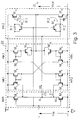
Images


Classifications
-
- H—ELECTRICITY
- H03—ELECTRONIC CIRCUITRY
- H03K—PULSE TECHNIQUE
- H03K19/00—Logic circuits, i.e. having at least two inputs acting on one output; Inverting circuits
- H03K19/003—Modifications for increasing the reliability for protection
- H03K19/00346—Modifications for eliminating interference or parasitic voltages or currents
- H03K19/00361—Modifications for eliminating interference or parasitic voltages or currents in field effect transistor circuits
-
- H—ELECTRICITY
- H03—ELECTRONIC CIRCUITRY
- H03K—PULSE TECHNIQUE
- H03K17/00—Electronic switching or gating, i.e. not by contact-making and –breaking
- H03K17/16—Modifications for eliminating interference voltages or currents
- H03K17/161—Modifications for eliminating interference voltages or currents in field-effect transistor switches
- H03K17/165—Modifications for eliminating interference voltages or currents in field-effect transistor switches by feedback from the output circuit to the control circuit
- H03K17/166—Soft switching
-
- H—ELECTRICITY
- H03—ELECTRONIC CIRCUITRY
- H03K—PULSE TECHNIQUE
- H03K19/00—Logic circuits, i.e. having at least two inputs acting on one output; Inverting circuits
- H03K19/003—Modifications for increasing the reliability for protection
- H03K19/00369—Modifications for compensating variations of temperature, supply voltage or other physical parameters
- H03K19/00384—Modifications for compensating variations of temperature, supply voltage or other physical parameters in field effect transistor circuits
Definitions
- the present invention relates to an output buffer for digital signals as defined in the preamble of Claim 1.
- output buffers for digital signals for example, in data-transmission circuits and in multi-output digital circuits (such as RAMs, ROMs and EEPROMs with microprocessors) two problems in particular have to be addressed.
- ground bouncing is due to the simultaneous switching of many output stages.
- very high pulsed currents pass through the parasitic resistances and inductances associated with the electrical connections between the integrated circuit and the external terminals, that is, the interconnection wires and the metal strips of the terminal conductors.
- These transient currents cause variations in the supply potentials (ground and VDD) which may give rise to spurious internal switching and hence to loss or alteration of the data associated with the digital signal.
- Another effect of the transient currents is the emission of intense, high-frequency electromagnetic radiation which may interfere with other circuits in the integrated device and which may also be propagated into the surrounding environment, contributing to the emission of potentially harmful radiation.
- the other problem relates to the transmission of digital signals on lines outside the integrated circuit. If the line is not perfectly matched, which almost always occurs to a more or less marked extent with wide-band transmission, a very rapid transition between the two levels of the digital signal, that is, a stepped signal with a very steep front causes a reflected wave. With a high degree of mismatch, the reflected wave may interfere with the signal to the extent of preventing its correct transmission.
- a known output buffer which reduces the rate of transition of the output signal is illustrated in Figure 1.
- the buffer is constituted by three pairs of complementary MOS transistors (M1n, M1p; M2n, M2p; M3n, M3p) which are connected in a push-pull arrangement between two supply terminals, indicated by the ground symbol and +VDD, and which have their drain electrodes connected together to an output terminal 10.
- the gate electrode of each transistor is connected to a separate terminal of a generator 11 for generating phase-shifted voltages.
- the input 12 of the generator is also the input of the buffer.
- the input signal Vin changes from a low logic state to a high logic state
- a potential is thus established at the gate electrodes of the p-channel transistors such as to make the transistors M1p, M2p, M3p conductive one after another whilst the transistors M1n, M2n, M3n remain non-conductive.
- the object of the present invention is to provide an output buffer which can provide a digital output signal with edges having shallower slopes than the edges of the digital input signal and in which the slopes can be set precisely.
- FIG. 2 shows an inverter INV1 to which a digital input signal Vin is applied and which emits a corresponding output signal in the form of a current Ibi, a current-adding node A which adds a regulating current -If to the current Ibi coming from the inverter INV1, and a low-pass filter 20 which is constituted by a resistor R and by a capacitor C and which receives the current sum Idr as an input and supplies a voltage Vdr to the input of a second inverter INV2.
- the output 21 of the inverter INV2 is the output of the buffer and is connected to a circuit block 22 which can produce the differential of the output voltage Vout and multiply it by a constant K to produce the regulating current -If.
- the input 23 of the adder A may be considered as the true input of the buffer and the current Ibi as the electrical quantity input into the buffer.
- the electrical output quantity is the voltage Vout.
- the block 22 performs a measurement of the slope of the edge of the output signal and supplies it to the adder as a current If with the opposite sign to the sign of the input current Ibi.
- the resulting current Idr is applied to the low-pass filter 20 the output voltage of which is the input Vdr of the second inverter INV2.
- the circuit block 22 establishes a negative feedback which has the effect of stabilizing the slope of the edges of the output voltage and reducing its dependence on variations due to the process and to the supply and, partially, on variations due to the load and to the temperature.
- circuit diagram of Figure 3 shows a practical embodiment of the buffer according to the invention. Although a precise identification of the blocks of the diagram of Figure 2 in the circuit diagram of Figure 3 is not possible, for reasons which will become clear from the following description, various parts of the circuit are enclosed by broken lines and indicated by the symbols and the reference numbers used in Figure 2 to show how the block diagram and the circuit diagram correspond.
- the inverter INV1 is constituted by two complementary MOS transistors M1 (n-channel) and M2 (p-channel) which are connected between the supply terminals, indicated +VDD and by the ground symbol, and which have their gate electrodes connected together to the input terminal of the circuit and their drain electrodes connected together to the input 23 of the buffer.
- the inverter INV2 is constituted by two complementary MOS transistors, that is, an n-channel MOS transistor M15 and a p-channel MOS transistor M16 connected in a push-pull arrangement between the supply terminals.
- the transistors M15 and M16 have their drain electrodes connected together to the output terminal 21 of the buffer and their gate electrodes connected to the input 23 of the buffer, each via a resistive unit identified R1, R2, respectively.
- the unit R1 is constituted by a resistor R1' and by a p-channel MOS transistor M13 connected in parallel with the resistor and the unit R2 is constituted by a resistor R2' and by an n-channel MOS transistor M14 connected in parallel with the resistor.
- the gate electrodes of the transistors M13 and M14 are connected together to the input of the inverter INV1.
- resistive units R1 and R2 are included in the block indicated as the inverter INV2, they form part of the low-pass filter indicated 20 in Figure 2.
- the parasitic input capacitances Cp and Cn of the transistors M16 and M15, which also form part of the low-pass filter 20 (and correspond to the capacitor C of Figure 2), are included in the same block.
- the differentiating circuit 22 is constituted by two capacitive elements formed, in this embodiment, by the gate-channel capacitances of two MOS transistors, a p-channel MOS transistor M10 and an n-channel MOS transistor M11, and by two capacitance multipliers constituted by four current mirrors MR1, MR2, MR3, MR4 having a predetermined gain, for example, of 2, connected as shown in the diagram of Figure 3.
- the transistor M1 of the inverter INV1 becomes conductive and the transistor M2 becomes non-conductive.
- the transistor M15 becomes non-conductive and transistor M16 becomes conductive.
- the output Vout of the inverter INV2, that is, the output of the buffer has the same sign as the input Vin but the slope of the leading edge is less than that of the input signal because the switching of the transistor M16 of the inverter INV2 which changes from non-conduction to conduction, is slowed by the charging of the input capacitance Cp through the resistive element R1.
- the resistance of the resistive element R1 depends on the conduction state of the transistor M13; in the embodiment described above, the gate electrode of the transistor M13 changes from a low level to a high level so that the transistor M13 becomes non-conductive and the resistance of the resistive element R1 is, in practice, that of the resistor R1'.
- the transistor M14 of the resistive element R2 which is an n-channel transistor, is made conductive by the same signal which controls the transistor M13.
- the transistor M14 thus becomes conductive so that the resistance of the resistive element R2 is practically zero (the resistance of the transistor M14 when it is conductive); this has the effect of a rapid switching of the transistor M15 (from conduction to non-conduction) so that the effect of slowing of the transition of the signal from the low level to the high level caused by the charging of the capacitance Cp through the resistor R1' is not affected.
- the operation of the circuit when the signal Vin has a transition from the high level to the low level is exactly the same but with the opposite sign.
- a current If of a magnitude dependent on the transition time is added, in the adding node A, to the input current Ibi supplied by one or other of the transistors M1, M2 of the inverter INV1 (in this example by M1).
- the sign of this current is always the opposite of that of the input current, owing to the crossed connection of the current mirrors.
- the current mirrors MR3 and MR2 constitute the path between the capacitance of M11 and the input and the current mirrors MR4 and MR1 constitute the path between the capacitance of M10 and the input.
- the buffer according to the invention not only enables the slope of the edges of the digital signal to be regulated automatically and precisely, rendering it substantially independent of variations due to the process by which the integrated circuit is produced and to environmental operating conditions, but can also be produced in a smaller area than is required by a known buffer with known regulation, such as that shown in Figure 1.
- resistors of constant resistance could be used instead of the resistive units R1 and R2, the resistance of which is dependent on the input signal, and true capacitors could be used instead of the capacitive units constituted by MOS transistors and capacitance multipliers.
Abstract
The buffer comprises means (20) for reducing the
slope of the input signal (Vin) and a negative feedback
circuit (22) which generates a regulating signal
dependent on the variation of the output signal (Vout)
and applies the regulating signal (If) to the input of
the buffer.
A precise regulation of the slope, independent of
variations in the production process and of environmental
conditions, is achieved.
Description
- The present invention relates to an output buffer for digital signals as defined in the preamble of
Claim 1. - In some applications of output buffers for digital signals, for example, in data-transmission circuits and in multi-output digital circuits (such as RAMs, ROMs and EEPROMs with microprocessors) two problems in particular have to be addressed.
- One of these problems, so-called "ground bouncing" is due to the simultaneous switching of many output stages. In this situation, very high pulsed currents pass through the parasitic resistances and inductances associated with the electrical connections between the integrated circuit and the external terminals, that is, the interconnection wires and the metal strips of the terminal conductors. These transient currents cause variations in the supply potentials (ground and VDD) which may give rise to spurious internal switching and hence to loss or alteration of the data associated with the digital signal. Another effect of the transient currents is the emission of intense, high-frequency electromagnetic radiation which may interfere with other circuits in the integrated device and which may also be propagated into the surrounding environment, contributing to the emission of potentially harmful radiation.
- The other problem relates to the transmission of digital signals on lines outside the integrated circuit. If the line is not perfectly matched, which almost always occurs to a more or less marked extent with wide-band transmission, a very rapid transition between the two levels of the digital signal, that is, a stepped signal with a very steep front causes a reflected wave. With a high degree of mismatch, the reflected wave may interfere with the signal to the extent of preventing its correct transmission.
- A known output buffer which reduces the rate of transition of the output signal is illustrated in Figure 1. The buffer is constituted by three pairs of complementary MOS transistors (M1n, M1p; M2n, M2p; M3n, M3p) which are connected in a push-pull arrangement between two supply terminals, indicated by the ground symbol and +VDD, and which have their drain electrodes connected together to an
output terminal 10. The gate electrode of each transistor is connected to a separate terminal of agenerator 11 for generating phase-shifted voltages. Theinput 12 of the generator is also the input of the buffer. - When, for example, the input signal Vin changes from a low logic state to a high logic state, three signals V1p, V2p, V3p identical to the input signal Vin but delayed in sequence by a predetermined period of time, and three signals V1n, V2n, V3n all at the reference (ground) potential, appear at the outputs of the generator. A potential is thus established at the gate electrodes of the p-channel transistors such as to make the transistors M1p, M2p, M3p conductive one after another whilst the transistors M1n, M2n, M3n remain non-conductive. An increasing current due to the successive conduction of the transistors M1p, M2p and M3p will thus pass through the load (not shown) connected to the output of the buffer and a voltage step with an amplitude of approximately VDD, with a leading edge less steep than that of the input signal Vin will be formed at the
output 10. Similarly, a transition of the input signal Vin from a high logic state to a low logic state will bring about successive conduction of the transistors M1n, M2n and M3n and hence the formation at theoutput 10 of a voltage step with an amplitude of approximately VDD, with a trailing edge less steep than that of the input signal Vin. - Although the known arrangement described above is sound in principle, in practice, it can be used only in non-critical applications because the slope of the edges of the output signal cannot be determined with sufficient accuracy at the design stage. This disadvantage is due both to the variability of the parameters of the production process, as a result of which the delay times of the signals to be applied in sequence to the gate electrodes of the transistors cannot be predetermined with certainty, and to the dependence of the parameters which cause the delays on environmental operating conditions (particularly temperature).
- The object of the present invention is to provide an output buffer which can provide a digital output signal with edges having shallower slopes than the edges of the digital input signal and in which the slopes can be set precisely.
- This object is achieved by the provision of the output buffer defined and characterized in
Claim 1. - The invention will be understood better from the following detailed description of an embodiment thereof described by way of non-limiting example with reference to the appended drawings, in which:
- Figure 1 is a circuit diagram of a known output buffer,
- Figure 2 is a block diagram of an output buffer according to the invention, and
- Figure 3 is a circuit diagram of an output buffer according to the invention.
-
- The block diagram of Figure 2 shows an inverter INV1 to which a digital input signal Vin is applied and which emits a corresponding output signal in the form of a current Ibi, a current-adding node A which adds a regulating current -If to the current Ibi coming from the inverter INV1, and a low-
pass filter 20 which is constituted by a resistor R and by a capacitor C and which receives the current sum Idr as an input and supplies a voltage Vdr to the input of a second inverter INV2. Theoutput 21 of the inverter INV2 is the output of the buffer and is connected to acircuit block 22 which can produce the differential of the output voltage Vout and multiply it by a constant K to produce the regulating current -If. In this embodiment, theinput 23 of the adder A may be considered as the true input of the buffer and the current Ibi as the electrical quantity input into the buffer. The electrical output quantity is the voltage Vout. - In operation, the
block 22 performs a measurement of the slope of the edge of the output signal and supplies it to the adder as a current If with the opposite sign to the sign of the input current Ibi. The resulting current Idr is applied to the low-pass filter 20 the output voltage of which is the input Vdr of the second inverter INV2. Thecircuit block 22 establishes a negative feedback which has the effect of stabilizing the slope of the edges of the output voltage and reducing its dependence on variations due to the process and to the supply and, partially, on variations due to the load and to the temperature. - The circuit diagram of Figure 3 shows a practical embodiment of the buffer according to the invention. Although a precise identification of the blocks of the diagram of Figure 2 in the circuit diagram of Figure 3 is not possible, for reasons which will become clear from the following description, various parts of the circuit are enclosed by broken lines and indicated by the symbols and the reference numbers used in Figure 2 to show how the block diagram and the circuit diagram correspond.
- The inverter INV1 is constituted by two complementary MOS transistors M1 (n-channel) and M2 (p-channel) which are connected between the supply terminals, indicated +VDD and by the ground symbol, and which have their gate electrodes connected together to the input terminal of the circuit and their drain electrodes connected together to the
input 23 of the buffer. - The inverter INV2 is constituted by two complementary MOS transistors, that is, an n-channel MOS transistor M15 and a p-channel MOS transistor M16 connected in a push-pull arrangement between the supply terminals. The transistors M15 and M16 have their drain electrodes connected together to the
output terminal 21 of the buffer and their gate electrodes connected to theinput 23 of the buffer, each via a resistive unit identified R1, R2, respectively. The unit R1 is constituted by a resistor R1' and by a p-channel MOS transistor M13 connected in parallel with the resistor and the unit R2 is constituted by a resistor R2' and by an n-channel MOS transistor M14 connected in parallel with the resistor. The gate electrodes of the transistors M13 and M14 are connected together to the input of the inverter INV1. - It will be noted that, although the resistive units R1 and R2 are included in the block indicated as the inverter INV2, they form part of the low-pass filter indicated 20 in Figure 2. The parasitic input capacitances Cp and Cn of the transistors M16 and M15, which also form part of the low-pass filter 20 (and correspond to the capacitor C of Figure 2), are included in the same block.
- The differentiating
circuit 22 is constituted by two capacitive elements formed, in this embodiment, by the gate-channel capacitances of two MOS transistors, a p-channel MOS transistor M10 and an n-channel MOS transistor M11, and by two capacitance multipliers constituted by four current mirrors MR1, MR2, MR3, MR4 having a predetermined gain, for example, of 2, connected as shown in the diagram of Figure 3. - In order to examine the operation of the circuit, a transition of the signal Vin from the low level to the high level will be considered. The transistor M1 of the inverter INV1 becomes conductive and the transistor M2 becomes non-conductive. In the inverter INV2 which is controlled by the output of the inverter INV1, on the other hand, the transistor M15 becomes non-conductive and transistor M16 becomes conductive. The output Vout of the inverter INV2, that is, the output of the buffer, has the same sign as the input Vin but the slope of the leading edge is less than that of the input signal because the switching of the transistor M16 of the inverter INV2 which changes from non-conduction to conduction, is slowed by the charging of the input capacitance Cp through the resistive element R1.
- It will be noted that the resistance of the resistive element R1 depends on the conduction state of the transistor M13; in the embodiment described above, the gate electrode of the transistor M13 changes from a low level to a high level so that the transistor M13 becomes non-conductive and the resistance of the resistive element R1 is, in practice, that of the resistor R1'. At the same time, the transistor M14 of the resistive element R2, which is an n-channel transistor, is made conductive by the same signal which controls the transistor M13. The transistor M14 thus becomes conductive so that the resistance of the resistive element R2 is practically zero (the resistance of the transistor M14 when it is conductive); this has the effect of a rapid switching of the transistor M15 (from conduction to non-conduction) so that the effect of slowing of the transition of the signal from the low level to the high level caused by the charging of the capacitance Cp through the resistor R1' is not affected. The operation of the circuit when the signal Vin has a transition from the high level to the low level is exactly the same but with the opposite sign.
- The operation of the
negative feedback circuit 22 during a transition of the output signal will now be considered. During the transition, for example, from the low level to the high level, a current If of a magnitude dependent on the transition time is added, in the adding node A, to the input current Ibi supplied by one or other of the transistors M1, M2 of the inverter INV1 (in this example by M1). The sign of this current is always the opposite of that of the input current, owing to the crossed connection of the current mirrors. In particular, the current mirrors MR3 and MR2 constitute the path between the capacitance of M11 and the input and the current mirrors MR4 and MR1 constitute the path between the capacitance of M10 and the input. - It has been found that the buffer according to the invention not only enables the slope of the edges of the digital signal to be regulated automatically and precisely, rendering it substantially independent of variations due to the process by which the integrated circuit is produced and to environmental operating conditions, but can also be produced in a smaller area than is required by a known buffer with known regulation, such as that shown in Figure 1.
- Although only one embodiment of the present invention has been described and illustrated, clearly many variations and modifications are possible within the scope of the same inventive concept. For example, resistors of constant resistance could be used instead of the resistive units R1 and R2, the resistance of which is dependent on the input signal, and true capacitors could be used instead of the capacitive units constituted by MOS transistors and capacitance multipliers.
Claims (8)
- An output buffer for digital signals defined by transitions between two levels of an electrical quantity (Vin) applied as an input to the buffer, comprising slope-variation means (20) for generating an electrical output quantity (Vout) corresponding to the electrical input quantity but having transition times longer than those of the electrical input quantity, characterized by a negative feedback circuit comprising means (22) for generating a regulating signal (If) dependent on the variation of the electrical output quantity (Vout), and means (A) for applying the regulating signals to the input of the buffer.
- A buffer according to Claim 1, in which the means for generating a regulating signal comprise a circuit (22) which produces the time differential of the electrical output quantity (Vout), and the means for applying the regulating signals to the input of the buffer comprise an adder (A).
- A buffer according to Claim 1 or Claim 2, in which the slope variation means (20) comprise a low-pass filter (R, C).
- A buffer according to Claim 3, comprising an inverter (INV2) having two complementary MOS transistors (M15, M16) connected in a push-pull arrangement between two supply terminals with their drain electrodes connected to an output terminal (21) of the buffer and with their gate electrodes connected, via two respective resistive elements (R1, M13; R2, M14), to an input terminal (23) of the buffer, in which the low-pass filter comprises the resistive elements and the input capacitances (Cp, Cn) of the two MOS transistors (M15, M16).
- A buffer according to Claim 4, in which the circuit (22) which produces the differential comprises capacitive means (M10, M11, MR1-4) connected between the output terminal (21) and the input terminal (23) of the buffer.
- A buffer according to Claim 5, in which the capacitive means comprise two MOS transistors (M10, M11) each connected so as to act as a capacitor, and two capacitance multipliers (MR1-MR4) associated therewith.
- A buffer according to Claim 6, in which each of the two capacitance multipliers comprises two current mirrors (MR1-MR4).
- A buffer according to any one of Claims 4 to 7, in which each of the two resistive elements comprises a resistor (R1, R2) and a MOS transistor (M13, M14) connected in parallel with the resistor, and in which means (INV1) are provided for controlling the conduction states of the MOS transistors (M13, M14) in parallel with the resistors, in counterphase with one another and in synchronism with the electrical input quantity.
Priority Applications (2)
| Application Number | Priority Date | Filing Date | Title |
|---|---|---|---|
| EP99830634A EP1091492A1 (en) | 1999-10-08 | 1999-10-08 | An output buffer for digital signals |
| US09/684,157 US6545503B1 (en) | 1999-10-08 | 2000-10-06 | Output buffer for digital signals |
Applications Claiming Priority (1)
| Application Number | Priority Date | Filing Date | Title |
|---|---|---|---|
| EP99830634A EP1091492A1 (en) | 1999-10-08 | 1999-10-08 | An output buffer for digital signals |
Publications (1)
| Publication Number | Publication Date |
|---|---|
| EP1091492A1 true EP1091492A1 (en) | 2001-04-11 |
Family
ID=8243619
Family Applications (1)
| Application Number | Title | Priority Date | Filing Date |
|---|---|---|---|
| EP99830634A Withdrawn EP1091492A1 (en) | 1999-10-08 | 1999-10-08 | An output buffer for digital signals |
Country Status (2)
| Country | Link |
|---|---|
| US (1) | US6545503B1 (en) |
| EP (1) | EP1091492A1 (en) |
Cited By (3)
| Publication number | Priority date | Publication date | Assignee | Title |
|---|---|---|---|---|
| WO2003073451A2 (en) * | 2002-02-21 | 2003-09-04 | Broadcom Corporation | Methods and systems for providing load-adaptive output current drive |
| EP1880469A2 (en) * | 2005-05-13 | 2008-01-23 | Packet Digital | Controlling transient current peaks |
| CN108563276A (en) * | 2018-06-01 | 2018-09-21 | 电子科技大学 | A kind of high speed Voltage Reference Buffer with cross-couplings filter network |
Families Citing this family (3)
| Publication number | Priority date | Publication date | Assignee | Title |
|---|---|---|---|---|
| US7521975B2 (en) * | 2005-01-20 | 2009-04-21 | Advanced Micro Devices, Inc. | Output buffer with slew rate control utilizing an inverse process dependent current reference |
| DE102005028173B4 (en) * | 2005-06-17 | 2007-03-08 | Texas Instruments Deutschland Gmbh | Integrated CMOS duty cycle correction circuit for a clock signal |
| US10958271B1 (en) | 2020-07-07 | 2021-03-23 | Micron Technology, Inc. | Output buffer having supply filters |
Citations (4)
| Publication number | Priority date | Publication date | Assignee | Title |
|---|---|---|---|---|
| US5041741A (en) * | 1990-09-14 | 1991-08-20 | Ncr Corporation | Transient immune input buffer |
| WO1991020129A1 (en) * | 1990-06-12 | 1991-12-26 | Robert Bosch Gmbh | Circuit for limiting the rate of increase in the signal level of output signals of integrated circuits |
| US5111076A (en) * | 1990-09-05 | 1992-05-05 | Min Ming Tarng | Digital superbuffer |
| EP0678983A1 (en) * | 1994-04-22 | 1995-10-25 | STMicroelectronics S.r.l. | Output buffer current slew rate control integrated circuit |
Family Cites Families (4)
| Publication number | Priority date | Publication date | Assignee | Title |
|---|---|---|---|---|
| JPH07245546A (en) * | 1994-03-03 | 1995-09-19 | Nippon Motorola Ltd | Active low pass filter |
| US5543753A (en) * | 1994-06-22 | 1996-08-06 | Carver Corporation | Audio frequency power amplifiers with actively damped filter |
| US5805020A (en) * | 1996-06-27 | 1998-09-08 | Harris Corporation | Silent start class D amplifier |
| JP3745123B2 (en) * | 1998-08-24 | 2006-02-15 | 三菱電機株式会社 | Duty ratio correction circuit and clock generation circuit |
-
1999
- 1999-10-08 EP EP99830634A patent/EP1091492A1/en not_active Withdrawn
-
2000
- 2000-10-06 US US09/684,157 patent/US6545503B1/en not_active Expired - Lifetime
Patent Citations (4)
| Publication number | Priority date | Publication date | Assignee | Title |
|---|---|---|---|---|
| WO1991020129A1 (en) * | 1990-06-12 | 1991-12-26 | Robert Bosch Gmbh | Circuit for limiting the rate of increase in the signal level of output signals of integrated circuits |
| US5111076A (en) * | 1990-09-05 | 1992-05-05 | Min Ming Tarng | Digital superbuffer |
| US5041741A (en) * | 1990-09-14 | 1991-08-20 | Ncr Corporation | Transient immune input buffer |
| EP0678983A1 (en) * | 1994-04-22 | 1995-10-25 | STMicroelectronics S.r.l. | Output buffer current slew rate control integrated circuit |
Cited By (7)
| Publication number | Priority date | Publication date | Assignee | Title |
|---|---|---|---|---|
| WO2003073451A2 (en) * | 2002-02-21 | 2003-09-04 | Broadcom Corporation | Methods and systems for providing load-adaptive output current drive |
| WO2003073451A3 (en) * | 2002-02-21 | 2003-10-16 | Broadcom Corp | Methods and systems for providing load-adaptive output current drive |
| US6690199B2 (en) | 2002-02-21 | 2004-02-10 | Broadcom Corporation | Methods and systems for providing load-adaptive output current drive |
| US6859069B2 (en) | 2002-02-21 | 2005-02-22 | Broadcom Corporation | Methods and systems for providing load-adaptive output current drive |
| EP1880469A2 (en) * | 2005-05-13 | 2008-01-23 | Packet Digital | Controlling transient current peaks |
| EP1880469A4 (en) * | 2005-05-13 | 2008-06-11 | Packet Digital | Controlling transient current peaks |
| CN108563276A (en) * | 2018-06-01 | 2018-09-21 | 电子科技大学 | A kind of high speed Voltage Reference Buffer with cross-couplings filter network |
Also Published As
| Publication number | Publication date |
|---|---|
| US6545503B1 (en) | 2003-04-08 |
Similar Documents
| Publication | Publication Date | Title |
|---|---|---|
| US4479216A (en) | Skew-free clock circuit for integrated circuit chip | |
| KR100231091B1 (en) | Level shifter circuit | |
| US6642769B1 (en) | High speed voltage level shifter with a low input voltage | |
| US4305009A (en) | Low power consumption high speed transistor circuit comprising a complementary circuit | |
| KR20000070254A (en) | Zero-delay slew-rate controlled output buffer | |
| EP0086090B1 (en) | Drive circuit for capacitive loads | |
| JP3338758B2 (en) | Delay circuit | |
| US4785262A (en) | Pulse generator producing pulses having a width free from a power voltage and a threshold voltage of an inverter used therein | |
| JP2743878B2 (en) | Input buffer circuit | |
| JP4477705B2 (en) | Differential amplifier circuit | |
| EP0015554B1 (en) | Comparator circuit | |
| EP0069444B1 (en) | Trigger pulse generator | |
| EP1091492A1 (en) | An output buffer for digital signals | |
| US4472645A (en) | Clock circuit for generating non-overlapping pulses | |
| US6850100B2 (en) | Output buffer circuit | |
| US6346835B1 (en) | Power-on reset signal preparing circuit | |
| EP0845862A2 (en) | Circuit for removing noise components of oscillator | |
| JP2006526318A (en) | Improved resonant line drive circuit | |
| US4837463A (en) | Three-state complementary field effect integrated circuit | |
| EP1292031A2 (en) | Integrated circuit and method of adjusting capacitance of a node of an integrated circuit | |
| EP0720296A2 (en) | Buffer circuit and bias circuit | |
| WO1988008228A2 (en) | Method and apparatus for reducing transient noise in integrated circuits | |
| KR20010004448A (en) | An Invertor for outputting a high voltage | |
| JP3688072B2 (en) | Variable delay circuit | |
| KR100430973B1 (en) | Circuit for comparing two electrical quantities |
Legal Events
| Date | Code | Title | Description |
|---|---|---|---|
| PUAI | Public reference made under article 153(3) epc to a published international application that has entered the european phase |
Free format text: ORIGINAL CODE: 0009012 |
|
| AK | Designated contracting states |
Kind code of ref document: A1 Designated state(s): DE FR GB IT |
|
| AX | Request for extension of the european patent |
Free format text: AL;LT;LV;MK;RO;SI |
|
| 17P | Request for examination filed |
Effective date: 20010918 |
|
| AKX | Designation fees paid |
Free format text: DE FR GB IT |
|
| GRAP | Despatch of communication of intention to grant a patent |
Free format text: ORIGINAL CODE: EPIDOSNIGR1 |
|
| STAA | Information on the status of an ep patent application or granted ep patent |
Free format text: STATUS: THE APPLICATION IS DEEMED TO BE WITHDRAWN |
|
| 18D | Application deemed to be withdrawn |
Effective date: 20080219 |