EP1091419A1 - Potentiomètre intégré et procédé de fabrication correspondant - Google Patents
Potentiomètre intégré et procédé de fabrication correspondant Download PDFInfo
- Publication number
- EP1091419A1 EP1091419A1 EP00402686A EP00402686A EP1091419A1 EP 1091419 A1 EP1091419 A1 EP 1091419A1 EP 00402686 A EP00402686 A EP 00402686A EP 00402686 A EP00402686 A EP 00402686A EP 1091419 A1 EP1091419 A1 EP 1091419A1
- Authority
- EP
- European Patent Office
- Prior art keywords
- mos transistor
- drain
- source
- voltage
- transistor
- Prior art date
- Legal status (The legal status is an assumption and is not a legal conclusion. Google has not performed a legal analysis and makes no representation as to the accuracy of the status listed.)
- Pending
Links
- 238000004519 manufacturing process Methods 0.000 title description 2
- 239000000758 substrate Substances 0.000 claims abstract description 25
- 230000015556 catabolic process Effects 0.000 claims abstract description 18
- 230000003071 parasitic effect Effects 0.000 claims abstract description 16
- 230000002427 irreversible effect Effects 0.000 claims abstract description 9
- 238000000034 method Methods 0.000 claims abstract description 9
- 230000010287 polarization Effects 0.000 claims abstract description 5
- 230000000977 initiatory effect Effects 0.000 claims abstract 2
- 238000005538 encapsulation Methods 0.000 description 6
- XUIMIQQOPSSXEZ-UHFFFAOYSA-N Silicon Chemical compound [Si] XUIMIQQOPSSXEZ-UHFFFAOYSA-N 0.000 description 3
- 244000045947 parasite Species 0.000 description 3
- 230000002829 reductive effect Effects 0.000 description 3
- 229910052710 silicon Inorganic materials 0.000 description 3
- 239000010703 silicon Substances 0.000 description 3
- 235000012431 wafers Nutrition 0.000 description 3
- 230000002457 bidirectional effect Effects 0.000 description 2
- 230000003247 decreasing effect Effects 0.000 description 2
- 238000010586 diagram Methods 0.000 description 2
- 230000000694 effects Effects 0.000 description 2
- 230000002441 reversible effect Effects 0.000 description 2
- 230000000903 blocking effect Effects 0.000 description 1
- 239000000470 constituent Substances 0.000 description 1
- 239000013078 crystal Substances 0.000 description 1
- 230000006378 damage Effects 0.000 description 1
- 230000007547 defect Effects 0.000 description 1
- 230000001066 destructive effect Effects 0.000 description 1
- 230000000670 limiting effect Effects 0.000 description 1
- 238000004806 packaging method and process Methods 0.000 description 1
- 229910021420 polycrystalline silicon Inorganic materials 0.000 description 1
- 229920005591 polysilicon Polymers 0.000 description 1
- 229920006395 saturated elastomer Polymers 0.000 description 1
- 230000003313 weakening effect Effects 0.000 description 1
Images

Classifications
-
- H—ELECTRICITY
- H10—SEMICONDUCTOR DEVICES; ELECTRIC SOLID-STATE DEVICES NOT OTHERWISE PROVIDED FOR
- H10D—INORGANIC ELECTRIC SEMICONDUCTOR DEVICES
- H10D1/00—Resistors, capacitors or inductors
- H10D1/40—Resistors
- H10D1/47—Resistors having no potential barriers
-
- H—ELECTRICITY
- H10—SEMICONDUCTOR DEVICES; ELECTRIC SOLID-STATE DEVICES NOT OTHERWISE PROVIDED FOR
- H10D—INORGANIC ELECTRIC SEMICONDUCTOR DEVICES
- H10D1/00—Resistors, capacitors or inductors
- H10D1/40—Resistors
- H10D1/43—Resistors having PN junctions
-
- H—ELECTRICITY
- H10—SEMICONDUCTOR DEVICES; ELECTRIC SOLID-STATE DEVICES NOT OTHERWISE PROVIDED FOR
- H10D—INORGANIC ELECTRIC SEMICONDUCTOR DEVICES
- H10D84/00—Integrated devices formed in or on semiconductor substrates that comprise only semiconducting layers, e.g. on Si wafers or on GaAs-on-Si wafers
- H10D84/201—Integrated devices formed in or on semiconductor substrates that comprise only semiconducting layers, e.g. on Si wafers or on GaAs-on-Si wafers characterised by the integration of only components covered by H10D1/00 or H10D8/00, e.g. RLC circuits
- H10D84/204—Integrated devices formed in or on semiconductor substrates that comprise only semiconducting layers, e.g. on Si wafers or on GaAs-on-Si wafers characterised by the integration of only components covered by H10D1/00 or H10D8/00, e.g. RLC circuits of combinations of diodes or capacitors or resistors
- H10D84/209—Integrated devices formed in or on semiconductor substrates that comprise only semiconducting layers, e.g. on Si wafers or on GaAs-on-Si wafers characterised by the integration of only components covered by H10D1/00 or H10D8/00, e.g. RLC circuits of combinations of diodes or capacitors or resistors of only resistors
-
- H—ELECTRICITY
- H10—SEMICONDUCTOR DEVICES; ELECTRIC SOLID-STATE DEVICES NOT OTHERWISE PROVIDED FOR
- H10D—INORGANIC ELECTRIC SEMICONDUCTOR DEVICES
- H10D84/00—Integrated devices formed in or on semiconductor substrates that comprise only semiconducting layers, e.g. on Si wafers or on GaAs-on-Si wafers
- H10D84/40—Integrated devices formed in or on semiconductor substrates that comprise only semiconducting layers, e.g. on Si wafers or on GaAs-on-Si wafers characterised by the integration of at least one component covered by groups H10D12/00 or H10D30/00 with at least one component covered by groups H10D10/00 or H10D18/00, e.g. integration of IGFETs with BJTs
- H10D84/401—Combinations of FETs or IGBTs with BJTs
- H10D84/403—Combinations of FETs or IGBTs with BJTs and with one or more of diodes, resistors or capacitors
Definitions
- the present invention relates to the field of integrated circuits analog and digital. These circuits must use a surface of the lowest possible silicon in order to reduce costs while keeping high precision.
- the Applicant has noticed that the precision which is excellent during the step of sorting the silicon wafers, i.e. the removal of platelets with defects, may deteriorate during of the subsequent encapsulation step.
- the precision which is excellent during the step of sorting the silicon wafers i.e. the removal of platelets with defects
- the packaging for encapsulation creates a drift additional reducing the final offset voltage to 1.5 mV.
- the accuracy is 0.8%, reduced to 0.2% after adjustment.
- the housing introduces a drift reducing the final precision to 0.5%.
- the object of the present invention is therefore to be able to adjust the integrated circuits after they have been housed, in particular circuits standard integrated mass production and low cost.
- the goal is to obtain a very high precision, at least equal to that obtained after adjustment when sorting the wafers.
- the electrical resistance obtained is adjustable unidirectionally, its value being determined by the current of the at the first and second voltages and can be modified by application of other voltages with a higher current limitation, the first and second voltages being supplied by a generator with current limitation.
- one of the first and second voltage is constant, and the other voltage is a ramp to monotonous evolution.
- the application of first and second tensions take place before a step of encapsulation of a circuit of which the MOS transistor is a part.
- the application first and second tensions takes place after an encapsulation step of a circuit of which the MOS transistor is a part.
- the breakdown control of the MOS transistor can be performed by the conventional pins of the circuit integrated: ground, power supply, input (s), output (s).
- the present invention also relates to a component integrated active electronics, including a MOS transistor.
- Said MOS transistor is slammed by avalanche from the drain / substrate junction, polarization of the parasitic bipolar transistor of the MOS transistor, breakdown irreversible of the drain / substrate junction, and short circuit between the drain and the source, so that the said component forms an adjustable resistance of value determined by the current due to the voltage difference between drain and source of the MOS transistor.
- the present invention also relates to a circuit electronics comprising at least two components of the type described above to form an electric resistance so adjustable bidirectional.
- the circuit electronics includes a MOS transistor, a first component of the type described above arranged in parallel between the drain and the source of the MOS transistor, a second component of the type described above arranged between the gate of the MOS transistor and ground, and a current source placed between the grid and the power supply.
- the invention therefore makes it possible to propose integrated circuits standard of increased precision.
- MOS transistor called "snap-back) makes it possible to obtain a short circuit and therefore to vary a resistance inside an integrated circuit after its encapsulation in acting on the conventional pins of the integrated circuit.
- the component as well realized occupies only a small place on a silicon wafer in this meaning that it only includes a single MOS transistor.
- the fact that the grid and the source of the MOS transistor are short-circuited guarantees its blocking permanent and prevents it from affecting the operation of the circuits adjacent electronics.
- the invention highlights a natural characteristic of MOS transistors which is to possess parasitic components, in especially a bipolar transistor. In some configurations, these parasitic components are harmful. During electrostatic discharges, circuits can be seriously damaged by conduction of the parasitic transistor. Conversely, the invention uses the transistor parasitic bipolar of the MOS transistor to make a short circuit and make vary the resistance between the drain and the source of the MOS transistor, i.e. between the collector and the emitter of the parasitic bipolar transistor.
- an NMOS transistor has four operating regions. Region 1 is that of classic linear operation of a MOS transistor. Region 2 is that of operation in saturated mode where the current changes only very weakly depending on the voltage. Region 3 is called "avalanche" with a weakening of the drain / substrate junction caused by the avalanche of said junction. Finally, region 4 is that of the conduction of the parasitic bipolar transistor with a first break on the curve referenced 5 and which is reversible and a second break referenced 6 and which is destructive and therefore irreversible.
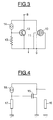
- FIGS 2 and 3 show the structure of the different constituents.
- the MOS transistor comprises a drain 8, a source 9 and a grid 10 formed on a substrate 11.
- a parasitic bipolar transistor 12 whose collector is formed by drain 8, whose transmitter is formed by the source 9 and whose base can be modeled as being connected to ground by a substrate resistor 13 and by a current source 14 connected to drain 8.
- the drain 8 is connected to a first supply voltage, while the source 9, the grid 10 and the substrate 11 are short-circuited and connected to a second voltage feed. From the saturation regime of the MOS transistor, a high voltage on the drain triggers the avalanche of the drain / substrate junction by generation of electron-hole pairs, thus creating a current of substrate. The voltage across the substrate resistance increases, thus polarizing the source / substrate junction. The bipolar transistor parasite is thus initiated, the phenomenon of breakage then occurs.
- the component At high current, the component returns to a second breaking regime irreversible and which results in a destruction of the crystal lattice of polysilicon of the channel formed between the drain and the source.
- the emitter After the avalanche of the collector-base junction of the parasitic bipolar transistor, the emitter connected to ground allows direct connection of the base-emitter, this which generates the reversal or snap-back effect.
- the current generator 14 which has been represented in FIGS. 2 and 3 between the collector and the base of the simulated parasitic bipolar transistor first the leakage currents of the drain / substrate junction. Subsequently, it simulates the avalanche of the junction and the polarization of the NPN parasitic bipolar transistor.
- transistors whose the channel is as short as possible since the shorter the channel, the lower the breakdown voltage, due to the increase in the drain current and increasing the number of electron-hole pairs generated, at constant channel width.
- a decrease in the width of channel results in a decrease in the voltage and current of the second break 6 illustrated in Figure 1. Even if the release of the channel does not intervene in the tension of the first break 5, a width reduced will increase the thermal effect of the second break 6 since the field lines are then more unidirectional, implying a decrease in the torque of the second break. It is therefore particularly interesting to use MOS transistors of small dimensions.
- a decrease in the resistance of component 16 occurs results in a decrease in the resistance of the whole of this circuit.
- a reduction in the resistance of component 17 results in a decrease in the gate voltage of the MOS transistor 15 and a increase in resistance between the drain and the source of said transistor MOS 15, this being in a linear region.
- the invention thus makes it possible to take advantage of a characteristic natural MOS transistors usually considered a drawback to make an integrated potentiometer which can be adjusted resistance value in a fine way to obtain integrated circuits produced in very large series and with high precision.
Landscapes
- Metal-Oxide And Bipolar Metal-Oxide Semiconductor Integrated Circuits (AREA)
- Semiconductor Integrated Circuits (AREA)
- Insulated Gate Type Field-Effect Transistor (AREA)
Abstract
Description
- avalanche de la jonction drain/substrat,
- polarisation du transistor bipolaire parasite du transistor MOS,
- claquage irréversible de la jonction drain/substrat,
- court-circuit entre le drain et la source.
Claims (9)
- Procédé pour obtenir une résistance électrique ajustable, dans lequel on applique à un transistor MOS intégré une première tension sur sa source, sa grille et son substrat, et une deuxième tension sur son drain, les première et deuxième tensions étant aptes à amorcer un claquage du transistor MOS par :avalanche de la jonction drain/substrat,polarisation du transistor bipolaire parasite du transistor MOS,claquage irréversible de la jonction drain/substrat,court-circuit entre le drain et la source.
- Procédé selon la revendication 1, dans lequel la résistance électrique obtenue est ajustable de façon unidirectionnelle, sa valeur étant déterminée par le courant du aux première et deuxième tensions et pouvant être modifiée par application d'autres tensions avec une limitation en courant plus élevée, les première et deuxième tensions étant fournies par un générateur avec limitation de courant.
- Procédé selon la revendication 1 ou 2, dans lequel l'une des première et deuxième tensions est constante, et l'autre tension est une rampe à évolution monotone.
- Procédé selon l'une des revendications précédentes, dans lequel l'application des première et deuxième tensions a lieu avant une étape d'encapsulation d'un circuit dont fait partie le transistor MOS.
- Procédé selon l'une des revendications 1 à 3, dans lequel l'application des première et deuxième tensions a lieu après une étape d'encapsulation d'un circuit dont fait partie le transistor MOS.
- Procédé selon la revendication 5, dans lequel la commande du claquage du transistor MOS est effectuée par les broches classiques du circuit intégré : masse, alimentation, entrée(s), sortie(s).
- Composant électronique actif intégré, comprenant un transistor MOS, caractérisé par le fait que le dit transistor MOS est claqué par avalanche de la jonction drain/substrat, polarisation du transistor bipolaire parasite (12) du transistor MOS, claquage irréversible de la jonction drain/substrat, et court-circuit entre le drain (8) et la source (9), de façon que le dit composant forme une résistance ajustable de valeur déterminée par le courant du à la différence de tension entre drain et source du transistor MOS.
- Circuit électronique, caractérisé par le fait qu'il comprend au moins deux composants (16, 17) selon la revendication 7 pour former une résistance électrique ajustable de façon bidirectionnelle.
- Circuit électronique selon la revendication 8, caractérisé par le fait qu'il comprend un transistor MOS (15), un premier composant (16) selon la revendication 7 disposé en parallèle entre le drain et la source du transistor MOS, un deuxième composant (17) selon la revendication 7 disposé entre la grille du transistor MOS et la masse, et une source de courant (18) disposée entre la grille et l'alimentation.
Applications Claiming Priority (2)
| Application Number | Priority Date | Filing Date | Title |
|---|---|---|---|
| FR9912381A FR2799885B1 (fr) | 1999-10-05 | 1999-10-05 | Potentiometre integre et procede de fabrication correspondant |
| FR9912381 | 1999-10-05 |
Publications (1)
| Publication Number | Publication Date |
|---|---|
| EP1091419A1 true EP1091419A1 (fr) | 2001-04-11 |
Family
ID=9550570
Family Applications (1)
| Application Number | Title | Priority Date | Filing Date |
|---|---|---|---|
| EP00402686A Pending EP1091419A1 (fr) | 1999-10-05 | 2000-09-29 | Potentiomètre intégré et procédé de fabrication correspondant |
Country Status (3)
| Country | Link |
|---|---|
| US (1) | US6377115B1 (fr) |
| EP (1) | EP1091419A1 (fr) |
| FR (1) | FR2799885B1 (fr) |
Families Citing this family (2)
| Publication number | Priority date | Publication date | Assignee | Title |
|---|---|---|---|---|
| CN105789330B (zh) * | 2014-12-25 | 2019-04-16 | 北大方正集团有限公司 | 半导体电阻 |
| CN105845738B (zh) * | 2015-01-15 | 2018-09-14 | 北大方正集团有限公司 | 高压电阻 |
Citations (3)
| Publication number | Priority date | Publication date | Assignee | Title |
|---|---|---|---|---|
| US3893085A (en) * | 1973-11-28 | 1975-07-01 | Ibm | Read mostly memory cell having bipolar and FAMOS transistor |
| US4146902A (en) * | 1975-12-03 | 1979-03-27 | Nippon Telegraph And Telephone Public Corp. | Irreversible semiconductor switching element and semiconductor memory device utilizing the same |
| EP0656690A2 (fr) * | 1993-12-02 | 1995-06-07 | Kabushiki Kaisha Toshiba | Circuit à transistors |
Family Cites Families (3)
| Publication number | Priority date | Publication date | Assignee | Title |
|---|---|---|---|---|
| US3818245A (en) * | 1973-01-05 | 1974-06-18 | Tokyo Shibaura Electric Co | Driving circuit for an indicating device using insulated-gate field effect transistors |
| US5270533A (en) * | 1992-06-23 | 1993-12-14 | Smiths Industries | Stabilization biasing circuit for avalanche photodiodes |
| FR2754652B1 (fr) * | 1996-10-16 | 1998-12-24 | Sgs Thomson Microelectronics | Circuit de commande au zero de tension d'un triac |
-
1999
- 1999-10-05 FR FR9912381A patent/FR2799885B1/fr not_active Expired - Fee Related
-
2000
- 2000-09-29 EP EP00402686A patent/EP1091419A1/fr active Pending
- 2000-10-04 US US09/678,711 patent/US6377115B1/en not_active Expired - Lifetime
Patent Citations (3)
| Publication number | Priority date | Publication date | Assignee | Title |
|---|---|---|---|---|
| US3893085A (en) * | 1973-11-28 | 1975-07-01 | Ibm | Read mostly memory cell having bipolar and FAMOS transistor |
| US4146902A (en) * | 1975-12-03 | 1979-03-27 | Nippon Telegraph And Telephone Public Corp. | Irreversible semiconductor switching element and semiconductor memory device utilizing the same |
| EP0656690A2 (fr) * | 1993-12-02 | 1995-06-07 | Kabushiki Kaisha Toshiba | Circuit à transistors |
Non-Patent Citations (1)
| Title |
|---|
| PAN T -W ET AL: "A 50-DB VARIABLE GAIN AMPLIFIER USING PARASITIC BIPOLAR TRANSISTORSIN CMOS", IEEE JOURNAL OF SOLID-STATE CIRCUITS,US,IEEE INC. NEW YORK, vol. 24, no. 4, 1 August 1989 (1989-08-01), pages 951 - 961, XP000066223, ISSN: 0018-9200 * |
Also Published As
| Publication number | Publication date |
|---|---|
| FR2799885B1 (fr) | 2002-01-11 |
| FR2799885A1 (fr) | 2001-04-20 |
| US6377115B1 (en) | 2002-04-23 |
Similar Documents
| Publication | Publication Date | Title |
|---|---|---|
| CH642451A5 (fr) | Dispositif detecteur de temperature. | |
| EP0006474A1 (fr) | Procédé de correction du coefficient en tension de résistances semi-conductrices diffusées ou implantées | |
| EP2913849B1 (fr) | Dispositif electronique avec transistor hemt polarisé en inverse | |
| EP3232479A1 (fr) | Structure de diode | |
| EP3627275A1 (fr) | Dispositif électronique capable de former un capteur de température ou une source de courant délivrant un courant indépendant de la température | |
| FR3009149A1 (fr) | Element a retard variable | |
| FR2825806A1 (fr) | Circuit de polarisation a point de fonctionnement stable en tension et en temperature | |
| EP2775529A2 (fr) | Transistor à effet tunnel | |
| EP3185288A1 (fr) | Procédé de fabrication d'un transistor jfet au sein d'un circuit intégré et circuit intégré correspondant | |
| FR2512589A1 (fr) | Resistance variable reglee par une tension pour circuit electronique | |
| FR2799885A1 (fr) | Potentiometre integre et procede de fabrication correspondant | |
| EP2560066B1 (fr) | Procédé d'ajustement d'une tension de référence sur la base d'un circuit band-gap | |
| WO2016050879A1 (fr) | Transistor à effet de champ avec contact de drain mixte optimisé et procédé de fabrication | |
| EP1384267B1 (fr) | Dispositif d'ajustement des circuits avant mise en boitier | |
| CH651160A5 (fr) | Amplificateur differentiel a transistors bipolaires realises en technologie cmos. | |
| FR2596202A1 (fr) | Structure de transistor npn equivalent a tension de claquage plus elevee que la tension de claquage intrinseque des transistors npn | |
| FR3058857A1 (fr) | Capteur d'images cmos a bruit reduit | |
| EP4297090A1 (fr) | Dispositif microélectronique à deux transistors à effet de champ | |
| WO2000077856A1 (fr) | Dispositif semi-conducteur a tension de seuil compensee et procede de fabrication | |
| WO2017055709A1 (fr) | Circuit electronique elementaire pour etage d'amplification ou de recopie de signaux analogiques | |
| EP1895596A1 (fr) | Cellule mémoire DRAM sans capacité constituée d'un dispositif de type MOSFET partiellement déserté comportant un isolant de grille en deux parties | |
| FR2890239A1 (fr) | Compensation des derives electriques de transistors mos | |
| EP1638146A2 (fr) | Circuit électronique à double alimentation et à moyens de protection contre les claquages, et moyens de protection correspondants | |
| FR2738682A1 (fr) | Dispositif de protection contre des surtensions | |
| FR3115631A1 (fr) | Composant semiconducteur de circuit intégré |
Legal Events
| Date | Code | Title | Description |
|---|---|---|---|
| PUAI | Public reference made under article 153(3) epc to a published international application that has entered the european phase |
Free format text: ORIGINAL CODE: 0009012 |
|
| AK | Designated contracting states |
Kind code of ref document: A1 Designated state(s): DE FR GB IT |
|
| AX | Request for extension of the european patent |
Free format text: AL;LT;LV;MK;RO;SI |
|
| RIN1 | Information on inventor provided before grant (corrected) |
Inventor name: DUFAZA, CHRISTIAN Inventor name: FOREL, CHRISTOPHE Inventor name: AUVERGNE, DANIEL Inventor name: LAVILLE SEBASTIEN |
|
| RIN1 | Information on inventor provided before grant (corrected) |
Inventor name: LAVILLE, SEBASTIEN Inventor name: AUVERGNE, DANIEL Inventor name: FOREL, CHRISTOPHE Inventor name: DUFAZA, CHRISTIAN |
|
| 17P | Request for examination filed |
Effective date: 20011011 |
|
| RAP1 | Party data changed (applicant data changed or rights of an application transferred) |
Owner name: STMICROELECTRONICS S.A. |
|
| AKX | Designation fees paid |
Free format text: DE FR GB IT |
|
| STAA | Information on the status of an ep patent application or granted ep patent |
Free format text: STATUS: THE APPLICATION IS DEEMED TO BE WITHDRAWN |
|
| D18D | Application deemed to be withdrawn (deleted) | ||
| 18D | Application deemed to be withdrawn |
Effective date: 20080401 |