EP1091370A2 - Magnetic optical member and method of producing the same - Google Patents
Magnetic optical member and method of producing the same Download PDFInfo
- Publication number
- EP1091370A2 EP1091370A2 EP00113874A EP00113874A EP1091370A2 EP 1091370 A2 EP1091370 A2 EP 1091370A2 EP 00113874 A EP00113874 A EP 00113874A EP 00113874 A EP00113874 A EP 00113874A EP 1091370 A2 EP1091370 A2 EP 1091370A2
- Authority
- EP
- European Patent Office
- Prior art keywords
- magnetic optical
- substrate
- heat
- thin film
- magnetic
- Prior art date
- Legal status (The legal status is an assumption and is not a legal conclusion. Google has not performed a legal analysis and makes no representation as to the accuracy of the status listed.)
- Withdrawn
Links
Images




Classifications
-
- H—ELECTRICITY
- H01—ELECTRIC ELEMENTS
- H01F—MAGNETS; INDUCTANCES; TRANSFORMERS; SELECTION OF MATERIALS FOR THEIR MAGNETIC PROPERTIES
- H01F10/00—Thin magnetic films, e.g. of one-domain structure
- H01F10/08—Thin magnetic films, e.g. of one-domain structure characterised by magnetic layers
- H01F10/10—Thin magnetic films, e.g. of one-domain structure characterised by magnetic layers characterised by the composition
- H01F10/18—Thin magnetic films, e.g. of one-domain structure characterised by magnetic layers characterised by the composition being compounds
- H01F10/20—Ferrites
- H01F10/24—Garnets
- H01F10/245—Modifications for enhancing interaction with electromagnetic wave energy
-
- G—PHYSICS
- G11—INFORMATION STORAGE
- G11B—INFORMATION STORAGE BASED ON RELATIVE MOVEMENT BETWEEN RECORD CARRIER AND TRANSDUCER
- G11B11/00—Recording on or reproducing from the same record carrier wherein for these two operations the methods are covered by different main groups of groups G11B3/00 - G11B7/00 or by different subgroups of group G11B9/00; Record carriers therefor
- G11B11/10—Recording on or reproducing from the same record carrier wherein for these two operations the methods are covered by different main groups of groups G11B3/00 - G11B7/00 or by different subgroups of group G11B9/00; Record carriers therefor using recording by magnetic means or other means for magnetisation or demagnetisation of a record carrier, e.g. light induced spin magnetisation; Demagnetisation by thermal or stress means in the presence or not of an orienting magnetic field
- G11B11/105—Recording on or reproducing from the same record carrier wherein for these two operations the methods are covered by different main groups of groups G11B3/00 - G11B7/00 or by different subgroups of group G11B9/00; Record carriers therefor using recording by magnetic means or other means for magnetisation or demagnetisation of a record carrier, e.g. light induced spin magnetisation; Demagnetisation by thermal or stress means in the presence or not of an orienting magnetic field using a beam of light or a magnetic field for recording by change of magnetisation and a beam of light for reproducing, i.e. magneto-optical, e.g. light-induced thermomagnetic recording, spin magnetisation recording, Kerr or Faraday effect reproducing
- G11B11/10582—Record carriers characterised by the selection of the material or by the structure or form
-
- G—PHYSICS
- G11—INFORMATION STORAGE
- G11B—INFORMATION STORAGE BASED ON RELATIVE MOVEMENT BETWEEN RECORD CARRIER AND TRANSDUCER
- G11B11/00—Recording on or reproducing from the same record carrier wherein for these two operations the methods are covered by different main groups of groups G11B3/00 - G11B7/00 or by different subgroups of group G11B9/00; Record carriers therefor
- G11B11/10—Recording on or reproducing from the same record carrier wherein for these two operations the methods are covered by different main groups of groups G11B3/00 - G11B7/00 or by different subgroups of group G11B9/00; Record carriers therefor using recording by magnetic means or other means for magnetisation or demagnetisation of a record carrier, e.g. light induced spin magnetisation; Demagnetisation by thermal or stress means in the presence or not of an orienting magnetic field
- G11B11/105—Recording on or reproducing from the same record carrier wherein for these two operations the methods are covered by different main groups of groups G11B3/00 - G11B7/00 or by different subgroups of group G11B9/00; Record carriers therefor using recording by magnetic means or other means for magnetisation or demagnetisation of a record carrier, e.g. light induced spin magnetisation; Demagnetisation by thermal or stress means in the presence or not of an orienting magnetic field using a beam of light or a magnetic field for recording by change of magnetisation and a beam of light for reproducing, i.e. magneto-optical, e.g. light-induced thermomagnetic recording, spin magnetisation recording, Kerr or Faraday effect reproducing
- G11B11/10582—Record carriers characterised by the selection of the material or by the structure or form
- G11B11/10584—Record carriers characterised by the selection of the material or by the structure or form characterised by the form, e.g. comprising mechanical protection elements
-
- G—PHYSICS
- G11—INFORMATION STORAGE
- G11B—INFORMATION STORAGE BASED ON RELATIVE MOVEMENT BETWEEN RECORD CARRIER AND TRANSDUCER
- G11B11/00—Recording on or reproducing from the same record carrier wherein for these two operations the methods are covered by different main groups of groups G11B3/00 - G11B7/00 or by different subgroups of group G11B9/00; Record carriers therefor
- G11B11/10—Recording on or reproducing from the same record carrier wherein for these two operations the methods are covered by different main groups of groups G11B3/00 - G11B7/00 or by different subgroups of group G11B9/00; Record carriers therefor using recording by magnetic means or other means for magnetisation or demagnetisation of a record carrier, e.g. light induced spin magnetisation; Demagnetisation by thermal or stress means in the presence or not of an orienting magnetic field
- G11B11/105—Recording on or reproducing from the same record carrier wherein for these two operations the methods are covered by different main groups of groups G11B3/00 - G11B7/00 or by different subgroups of group G11B9/00; Record carriers therefor using recording by magnetic means or other means for magnetisation or demagnetisation of a record carrier, e.g. light induced spin magnetisation; Demagnetisation by thermal or stress means in the presence or not of an orienting magnetic field using a beam of light or a magnetic field for recording by change of magnetisation and a beam of light for reproducing, i.e. magneto-optical, e.g. light-induced thermomagnetic recording, spin magnetisation recording, Kerr or Faraday effect reproducing
- G11B11/10582—Record carriers characterised by the selection of the material or by the structure or form
- G11B11/10586—Record carriers characterised by the selection of the material or by the structure or form characterised by the selection of the material
-
- H—ELECTRICITY
- H01—ELECTRIC ELEMENTS
- H01F—MAGNETS; INDUCTANCES; TRANSFORMERS; SELECTION OF MATERIALS FOR THEIR MAGNETIC PROPERTIES
- H01F10/00—Thin magnetic films, e.g. of one-domain structure
- H01F10/26—Thin magnetic films, e.g. of one-domain structure characterised by the substrate or intermediate layers
- H01F10/28—Thin magnetic films, e.g. of one-domain structure characterised by the substrate or intermediate layers characterised by the composition of the substrate
-
- H—ELECTRICITY
- H01—ELECTRIC ELEMENTS
- H01F—MAGNETS; INDUCTANCES; TRANSFORMERS; SELECTION OF MATERIALS FOR THEIR MAGNETIC PROPERTIES
- H01F41/00—Apparatus or processes specially adapted for manufacturing or assembling magnets, inductances or transformers; Apparatus or processes specially adapted for manufacturing materials characterised by their magnetic properties
- H01F41/14—Apparatus or processes specially adapted for manufacturing or assembling magnets, inductances or transformers; Apparatus or processes specially adapted for manufacturing materials characterised by their magnetic properties for applying magnetic films to substrates
- H01F41/18—Apparatus or processes specially adapted for manufacturing or assembling magnets, inductances or transformers; Apparatus or processes specially adapted for manufacturing materials characterised by their magnetic properties for applying magnetic films to substrates by cathode sputtering
- H01F41/186—Apparatus or processes specially adapted for manufacturing or assembling magnets, inductances or transformers; Apparatus or processes specially adapted for manufacturing materials characterised by their magnetic properties for applying magnetic films to substrates by cathode sputtering for applying a magnetic garnet film
-
- H—ELECTRICITY
- H01—ELECTRIC ELEMENTS
- H01F—MAGNETS; INDUCTANCES; TRANSFORMERS; SELECTION OF MATERIALS FOR THEIR MAGNETIC PROPERTIES
- H01F41/00—Apparatus or processes specially adapted for manufacturing or assembling magnets, inductances or transformers; Apparatus or processes specially adapted for manufacturing materials characterised by their magnetic properties
- H01F41/14—Apparatus or processes specially adapted for manufacturing or assembling magnets, inductances or transformers; Apparatus or processes specially adapted for manufacturing materials characterised by their magnetic properties for applying magnetic films to substrates
- H01F41/22—Heat treatment; Thermal decomposition; Chemical vapour deposition
-
- G—PHYSICS
- G02—OPTICS
- G02F—OPTICAL DEVICES OR ARRANGEMENTS FOR THE CONTROL OF LIGHT BY MODIFICATION OF THE OPTICAL PROPERTIES OF THE MEDIA OF THE ELEMENTS INVOLVED THEREIN; NON-LINEAR OPTICS; FREQUENCY-CHANGING OF LIGHT; OPTICAL LOGIC ELEMENTS; OPTICAL ANALOGUE/DIGITAL CONVERTERS
- G02F1/00—Devices or arrangements for the control of the intensity, colour, phase, polarisation or direction of light arriving from an independent light source, e.g. switching, gating or modulating; Non-linear optics
- G02F1/0009—Materials therefor
- G02F1/0036—Magneto-optical materials
Definitions
- the present invention relates to a magnetic optical member used in an optical isolator and an optical magnetic recording medium and the like, and to a method of producing the same.
- An optical isolator used in optical fiber communication systems generally includes, for example, a pair of polarizers and a Faraday rotator interposed between the pair of polarizers.
- the Faraday rotator has the Faraday effect (magneto-optical effect) and rotates a polarizing surface of incident light by 45 degrees, that is the Faraday rotational angle is set to 45 degrees.
- an optical device utilizing the above-mentioned magneto-optical effect such as an optical magnetic recording medium (an optical magnetic disk) and an optical switch has been greatly used.
- an optical magnetic recording medium an optical magnetic disk
- temperature of the optical magnetic recording medium is locally increased by irradiation with laser light and recording is made with an external magnetic field only in the local portion where coercive force was decreased by the temperature increase. Since the spot diameter of the laser light can be reduced to about its wavelength, that is, a submicron length or so by narrowing the light with a lens, high density recording can be performed when combined with a vertically magnetized film as a recording medium.
- the reproduction of information recorded on the optical magnetic recording medium utilizes the principle (Kerr effect) that when an optical magnetic recording medium is irradiated with linearly polarized laser light, rotation is made in mutually opposite directions depending on the direction of the polarizing surface to the reflected light, that is, depending on whether the direction is upward or downward with respect to the vertical direction to the film surface.
- On the optical magnetic recording medium an optical magnetic disk
- a laser light guiding groove is formed into a spiral shape so that minute recording bits can be correctly recorded and reproduced.
- the reproducing device optical magnetic disk drive
- the reproducing device is provided with an automatic focusing mechanism and an automatic tracking mechanism for tracking the laser light along the groove in the optical system (pick-up head).
- an optical magnetic recording medium having a large Kerr rotational angle for short wavelength laser light is required.
- rare earth iron garnet based materials for example, bismuth-substituted rare earth iron-garnet (BiYIG) and the like have a large Kerr rotation (magneto-optical effect) at the short wavelength, even if the recording spot diameter, that is, the recording area is reduced, a large signal can be obtained.
- BiYIG bismuth-substituted rare earth iron-garnet
- the crystal structure of the BiYIG is amorphous just after the film formation, and annealing treatment to enhance crystallinity at 600°C or more is needed for obtaining large Hc (and excellent magnetic optical characteristics).
- the optical magnetic recording medium is generally placed on a resin substrate, which is deformed by the above-mentioned heat treatment. Therefore, under the above circumstances, it is difficult to form the optical magnetic recording medium using a rare earth iron garnet based magnetic material, and an excellent magneto-optical effect that the rare earth iron garnet based material possesses cannot be utilized.
- the present invention has been made in view of the above-mentioned circumstances and, therefore, an object of the present invention is to provide a magnetic optical member that can obtain a large magneto-optical effect using a rare earth iron garnet based material, and a method of producing the same.
- a magnetic optical member is characterized by comprising a non-heat-resisting substrate on which a magnetic optical thin film made of crystalline rare earth iron garnet is formed.
- the magnetic optical member in the first aspect of the present invention is characterized in that there are provided two dielectric multi-layer films having a cyclic structure in which plural kinds of dielectric materials having different optical characteristics are alternately laminated with regularity in thickness, and in that the magnetic optical thin film is placed between the two dielectric multi-layer films.
- the magnetic optical member in the first or second aspect of the present invention is characterized in that the non-heat-resisting substrate is a thermoplastic resin substrate.
- the magnetic optical member in any one of the first to third aspects of the present invention is characterized in that the non-heat-resisting substrate is a tape-shaped, film-shaped, or sheet-shaped substrate.
- the magnetic optical member in any one of the first to fourth aspects of the present invention is characterized in that the magnetic optical thin film is capable of magnetic recording.
- a method of producing a magnetic optical member comprising: two dielectric multi-layer films having a cyclic structure in which plural kinds of dielectric materials having different optical characteristics are alternately laminated with regularity in thickness; a magnetic optical thin film of rare earth iron-garnet, placed between the two dielectric multi-layers; and a non-heat-resisting substrate on which the layers and film are formed, is characterized in that the magnetic optical thin film is crystallized without deforming the non-heat-resisting substrate by the pulse heating wherein infrared beam is intermittently irradiated.
- the method of producing a magnetic optical member in the sixth aspect of the present invention is characterized in that the magnetic optical thin film is heated without disordering the cyclic structure of the dielectric multi-layer films.
- the method of producing a magnetic optical member in the sixth or seventh aspect of the present invention is characterized in that the non-heat-resisting substrate is cooled during heating the magnetic optical thin film.
- the method of producing a magnetic optical member in the sixth aspect of the present invention is characterized by using, in place of the infrared beam, laser light having a wavelength with which the light is not absorbed in the non-heat-resisting substrate but is absorbed in the magnetic optical thin film.
- the method of producing a magnetic optical member in the ninth aspect of the present invention is characterized in that the laser light has a wavelength with which the light is not absorbed in the dielectric multi-layer film.
- the method of producing a magnetic optical member in the tenth aspect of the present invention is characterized in that scanning with the laser light is performed.
- the method of producing a magnetic optical member in any one of the sixth to eleventh aspects of the present invention is characterized in that the non-heat-resisting substrate is a thermoplastic resin substrate.
- the method of producing a magnetic optical member in any one of the sixth to twelfth aspects of the present invention is characterized in that the non-heat-resisting substrate is a tape-shaped, film-shaped, or sheet-shaped substrate.
- the method of producing a magnetic optical member in any one of the sixth to thirteenth aspects of the present invention is characterized in that the magnetic optical thin film is capable of magnetic recording.
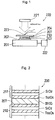
- an indium sheet 202 is set on a water-cooled substrate holder 201, a non-heat-resisting substrate 203 is placed on the indium sheet 202, and a glassy carbon 204 as a light condensing plate is set on the non-heat-resisting substrate 203.
- n layer 210 On the non-heat-resisting substrate 203 is laminated a (SiO 2 /Ta 2 O 5 ) n layer 210 (one of dielectric multi-layer films, n: the number of the laminated layers) in which a Ta 2 0 5 film (dielectric material) and a SiO 2 film (dielectric material) having different optical characteristics are alternately laminated with regularity in thickness.
- the Ta 2 0 5 film (dielectric material) and the SiO 2 film (dielectric material) are transparent in the visible ray region and are formed with an oxide having high environmental stability.
- the non-heat-resisting substrate 203 is made of a thermoplastic resin such as PMMA (polymethyl methacrylate) or PC (polycarbonate) or the like, and takes a tape shape, a film shape, or a sheet shape.
- a thermoplastic resin such as PMMA (polymethyl methacrylate) or PC (polycarbonate) or the like, and takes a tape shape, a film shape, or a sheet shape.
- n layer 210 is formed a bismuth substituted yttrium-iron-garnet thin film (BiYIG thin film) 207 (a magnetic optical thin film) which becomes capable of magnetic recording by heat treatment described later. Then, the BiYIG thin film 207 in this state is subjected to heat treatment for crystallization with an infrared ray introducing heater 220 as will be described later.
- BiYIG thin film bismuth substituted yttrium-iron-garnet thin film
- a sputtering device is used.
- the infrared ray introducing heater 220 includes an infrared ray generating portion 221 for generating an infrared beam, a glassy carbon 204 for condensing the infrared beam, a cooling mechanism 222 for cooling the substrate holder 201, and a thermocouple 223 that is placed in contact with the surface of the glassy carbon 204 and is used as a temperature monitor during heating.
- the non-heat-resisting substrate 203 and the (SiO 2 /Ta 2 O 5 ) n layer 210 are cooled through the substrate holder 201.
- the BiYIG thin film 207 is heated by the glassy carbon 204 whose temperature has been increased with infrared rays, to thereby crystallize the film and obtain excellent magnetic characteristics.
- the infrared beam is intermittently emitted (pulse-heated).
- the BiYIG thin film 207 is formed on the (SiO 2 /Ta 2 O 5 ) n layer 210 and is subjected to heat treatment for crystallization with infrared rays while cooling the non-heat-resisting substrate 203 and the (SiO 2 /Ta 2 O 5 ) n layer 210 through the substrate holder 201. Having been cooled, the non-heat-resisting substrate 203 is prevented from being deformed. Thus, heat treatment to crystallize the BiYIG thin film 207 can be performed.
- the BiYIG thin film 207 is crystallized by the above heat treatment, obtaining a large magneto-optical effect.
- thermoplastic resin substrate or a tape-shaped, film-shaped or sheet-shaped substrate can be used as the non-heat-resisting substrate 203, whereby easy handling of the substrate and downsizing can be realized.
- the (SiO 2 /Ta 2 O 5 ) n layer 210 is cooled as described above, preventing the interdiffusion of Ta 2 0 5 and SiO 2 in the (SiO 2 /Ta 2 O 5 ) n layer 210, so that the heat treatment for crystallization of the BiYIG thin film 207 can be performed. Further, by subjecting the BiYIG thin film 207 to heat treatment to crystallize, excellent magnetic characteristics are generated, resulting in the production of the one dimensional magnetic optical crystal 200 (one dimensional photonic crystal) having excellent magnetic optical characteristics. This one dimensional magnetic optical crystal 200 can be used as an optical magnetic recording medium, owing to the excellent magnetic characteristics of the BiYIG thin film 207 obtained through crystallization.
- the one dimensional magnetic optical crystal 200 of (SiO 2 /Ta 2 O 5 ) n /BiYIG/(Ta 2 O 5 /SiO 2 ) n structure can find another use such as an optical isolator by separating the non-heat-resisting substrate 203 joined thereto.
- the first embodiment takes as an example a case where the non-heat-resisting substrate 203 and the (SiO 2 /Ta 2 O 5 ) n layer 210 are cooled through the substrate holder 201.
- the non-heat-resisting substrate 203 and (SiO 2 /Ta 2 O 5 ) n layer 210 may be directly cooled.
- thermocouple 223 is allowed to contact with the surface of the glassy carbon 204 to monitor the temperature.
- the heat treatment pattern is shown in Fig. 3.
- the X ray diffraction pattern and the Faraday rotational angle when the member is subjected to the heat treatment for crystallization by such heat treatment are shown in Fig. 4 and Fig. 5, respectively.
- the BiYIG thin film 207 that has an amorphous structure immediately after the film formation, crystallization thereof progresses at a heat treatment temperature of 850 °C, and the Faraday rotational angle shows the same value as in the case where the film is heated and crystallized with a conventional electric furnace. Further, no surface roughening or a crack is found in the BiYIG thin film 207 at all.
- a substrate made of a thermoplastic resin such as PMMA (polymethyl methacrylate) and PC (polycarbonate) is heated by the same heating process to perform a preliminary experiment.
- PMMA polymethyl methacrylate
- PC polycarbonate
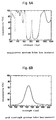
- heating treatment is performed on the multi-layer film having the (SiO 2 /Ta 2 O 5 ) n /(Ta 2 O 5 /SiO 2 ) n structure by the same heating process, and transmissivity spectrum is measured on the multi-layer film before heating and after heating.
- the results are shown in Figs. 6A, 6B and Figs. 7A, 7B.
- the design wavelength at this point is 750 nm and the thickness of each layer is ⁇ /4 of the optical wavelength.
- Fig. 6A shows a transmissivity spectrum before heat treatment
- Fig. 6B shows the peak wavelength spectrum (partially enlarged transmissivity spectrum in Fig. 6A).
- Fig. 7A shows a transmissivity spectrum after heat treatment
- Fig. 7B shows the peak wavelength spectrum in Fig. 7A (partially enlarged transmissivity spectrum in Fig. 7A).
- one dimensional magnetic optical crystal 200 (one dimensional photonic crystal) with the (SiO 2 /Ta 2 O 5 ) n /BiYIG/(Ta 2 O 5 /SiO 2 ) n structure which is formed by subjecting the (SiO 2 /Ta 2 O 5 ) n /BiYIG to heat treatment and depositing the (Ta 2 O 5 /SiO 2 ) n film thereon, the transmitted wavelength spectrum and Faraday rotational angle are measured. The results are shown in Fig. 8 and Fig. 9. As shown in Fig. 9, this one dimensional magnetic optical crystal 200 is found to have a large Faraday rotational angle.
- the infrared beam is adapted to be intermittently emitted (pulse heated), the crystallization of the BiYIG thin film 207 uniformly progresses to thereby obtain high accuracy.
- the infrared beam is condensed with the glassy carbon 204 to rapidly carry out the heat treatment.
- this embodiment may be configured so that the heat treatment is carried out without providing this glassy carbon 204.
- the first embodiment takes as an example the case where the heat treatment for crystallization of the BiYIG thin film 207 is carried out using infrared beam from the infrared ray introducing heater 220.
- the heat treatment for crystallization of the BiYIG thin film 207 may be carried out using laser light from a laser heater 230 (hereinafter referred to as a second embodiment) provided in place of the infrared ray introducing heater 220 as shown in Fig.10.
- a non-heat-resisting substrate 203 is set on a substrate holder 201 with one surface of which the (SiO 2 /Ta 2 O 5 ) n /BiYIG film is formed upward, and the (SiO 2 /Ta 2 O 5 ) n /BiYIG is irradiated with laser light from a laser light source 231 while scanning the laser light in a wide range to crystallize the BiYIG thin film 207.
- the laser light having a wavelength with which the light is not absorbed into the non-heat-resisting substrate 203 and the (SiO 2 /Ta 2 O 5 ) n layer 210 (dielectric multi-layer film) but is absorbed into the BiYIG thin film 207 (magnetic material film).
- the laser light having a wavelength with which the light is not absorbed into the non-heat-resisting substrate 203 and the (SiO 2 /Ta 2 O 5 ) n layer 210 (dielectric multi-layer film) but is absorbed into the BiYIG thin film 207 (magnetic material film).
- the (SiO 2 /Ta 2 O 5 ) n /BiYIG film is irradiated with the laser light having a wavelength with which the light is not absorbed into the non-heat-resisting substrate 203 and the (SiO 2 /Ta 2 O 5 ) n layer 210 (dielectric multi-layer film) but is absorbed into the BiYIG thin film 207 (magnetic material film), the (SiO 2 /Ta 2 O 5 ) n layer 210 (dielectric multi-layer film) is prevented from temperature rise also by the irradiation of the laser light, so that interdiffusion of Ta 2 0 5 and SiO 2 in (SiO 2 /Ta 2 O 5 ) n layer 210 is prevented.
- the BiYIG thin film 207 is heated by the irradiation of the laser light and is crystallized.
- the non-heat-resisting substrate 203 does not absorb the laser light and is prevented from temperature rise.
- a thermoplastic resin substrate or a tape-shaped, film-shaped, or sheet shaped substrate can be used, realizing easy handling of the substrate and downsizing.
- the crystallizing heat treatment of the BiYIG thin film 207 can be performed. Further, by subjecting the BiYIG thin film 207 to heat treatment to crystallize, excellent magnetic characteristics are generated and the one dimensional magnetic optical crystal 200 (one dimensional photonic crystal) having excellent magnetic optical characteristics is produced. This one dimensional magnetic optical crystal 200 can be used as an optical magnetic recording medium, owing to excellent magnetic characteristics of the BiYIG thin film 207 obtained through crystallization.
- the laser light is adapted to be intermittently emitted (pulse heated), crystallization of the BiYIG thin film 207 uniformly progresses to thereby obtain high accuracy.
- the (SiO 2 /Ta 2 O 5 ) n /BiYIG is irradiated with the laser light. Accordingly, heating of the BiYIG thin film 207 can rapidly progress, whereby improvement of the productivity can be attained.
- the cooling mechanism 222 and the cooling treatment which are required in the first embodiment are not needed. Therefore, the configuration of this embodiment becomes simpler and no cooling operation is needed, improving the productivity of the invention.
- the one dimensional magnetic optical crystal 200 which can be obtained in the first and second embodiments has the large Faraday effect as mentioned above, and can exhibit excellent functions when used in various optical devices such as an optical magnetic recording medium (optical magnetic recording disk) and an optical isolator.
- the first and second embodiments take as an example a case where the BiYIG thin film 207 is used.
- the present invention is not limited to this and can use other rare earth iron-garnet thin films.
- the magnetic optical member comprising a rare earth iron-garnet magnetic optical thin film and the crystalline magnetic optical thin film can exert excellent magneto-optical effects.
- the rare earth iron-garnet magnetic optical thin film is crystallized by pulse heating in which infrared beam is intermittently emitted without deforming the non-heat-resisting substrate.
- the non-heat-resisting substrate is formed with a thermoplastic resin, or in a tape shape, a film shape or a sheet shape, it can be further easily handled as compared with the case where a glass substrate is used, and can be reduced in size.
- the non-heat-resisting substrate a thermoplastic resin substrate or a tape-shaped, film-shaped, or sheet-shaped substrate can be used, whereby easy handling of the substrate and downsizing can be realized. Additionally, since a glass substrate is not required to use, the guiding groove for laser light is easy to form.
- the substrate is not limited to glass (heat-resisting member), making the member applicable in wider field, and improving the productivity of the invention.
Landscapes
- Engineering & Computer Science (AREA)
- Power Engineering (AREA)
- Physics & Mathematics (AREA)
- Manufacturing & Machinery (AREA)
- Electromagnetism (AREA)
- Chemical & Material Sciences (AREA)
- Materials Engineering (AREA)
- Thermal Sciences (AREA)
- Thin Magnetic Films (AREA)
- Manufacturing Of Magnetic Record Carriers (AREA)
- Optical Modulation, Optical Deflection, Nonlinear Optics, Optical Demodulation, Optical Logic Elements (AREA)
Abstract
Description
Claims (14)
- A magnetic optical member comprising a non-heat-resisting substrate on which a magnetic optical thin film of crystalline rare earth iron-garnet is formed.
- A magnetic optical member according to claim 1, wherein there are provided two dielectric multi-layer films having a cyclic structure in which plural kinds of dielectric materials having different optical characteristics are alternately laminated with regularity in thickness, and wherein said magnetic optical thin film is placed between said two dielectric multi-layer films.
- A magnetic optical member according to claim 1 or 2, wherein said non-heat-resisting substrate is a thermoplastic resin substrate.
- A magnetic optical member according to any one of claims 1 to 3, wherein said non-heat-resisting substrate is a tape-shaped, film-shaped, or sheet-shaped substrate.
- A magnetic optical member according to any one of claims 1 to 4, wherein said magnetic optical thin film is capable of magnetic recording.
- A method of producing a magnetic optical member comprising: two dielectric multi-layer films having a cyclic structure in which plural kinds of dielectric materials having different optical characteristics are alternately laminated with regularity in thickness; a magnetic optical thin film of rare earth iron-garnet placed between said two dielectric multi-layer films; and a non-heat-resisting substrate on which said film are formed, wherein said magnetic optical thin film is crystallized without deforming said non-heat-resisting substrate by the pulse heating of intermittent irradiation of infrared beam.
- A method of producing a magnetic optical member according to claim 6, wherein said magnetic optical thin film is heated without disordering the cyclic structure of said dielectric multi-layer films.
- A method of producing a magnetic optical member according to claim 6 or 7, wherein said non-heat-resisting substrate is cooled during heating the magnetic optical thin film.
- A method of producing a magnetic optical member according to claim 6, wherein laser light having a wavelength with which the light is not absorbed in said non-heat-resisting substrate but is absorbed in said magnetic optical thin film is used in place of the infrared beam.
- A method of producing a magnetic optical member according to claim 9, wherein said laser light has a wavelength with which the light is not absorbed in said dielectric multi-layer film.
- A method of producing a magnetic optical member according to claim 9 or 10, wherein scanning with the laser light is performed.
- A method of producing a magnetic optical member according to any one of claims 6 to 11, wherein said non-heat-resisting substrate is a thermoplastic resin substrate.
- A method of producing a magnetic optical member according to any one of claims 6 to 12, wherein said non-heat-resisting substrate is a tape-shaped, film-shaped, or sheet-shaped substrate.
- A method of producing a magnetic optical member according to anyone of claims 6 to 13, wherein said magnetic optical thin film is capable of magnetic recording.
Applications Claiming Priority (2)
| Application Number | Priority Date | Filing Date | Title |
|---|---|---|---|
| JP28351299A JP2001110635A (en) | 1999-10-04 | 1999-10-04 | Magneto-optical body and producing method therefor |
| JP28351299 | 1999-10-04 |
Publications (2)
| Publication Number | Publication Date |
|---|---|
| EP1091370A2 true EP1091370A2 (en) | 2001-04-11 |
| EP1091370A3 EP1091370A3 (en) | 2004-01-28 |
Family
ID=17666508
Family Applications (1)
| Application Number | Title | Priority Date | Filing Date |
|---|---|---|---|
| EP00113874A Withdrawn EP1091370A3 (en) | 1999-10-04 | 2000-06-30 | Magnetic optical member and method of producing the same |
Country Status (4)
| Country | Link |
|---|---|
| US (1) | US6743465B2 (en) |
| EP (1) | EP1091370A3 (en) |
| JP (1) | JP2001110635A (en) |
| CA (1) | CA2313768A1 (en) |
Cited By (1)
| Publication number | Priority date | Publication date | Assignee | Title |
|---|---|---|---|---|
| EP1102285A3 (en) * | 1999-10-27 | 2006-03-22 | Minebea Co., Ltd. | Magneto-optical member |
Families Citing this family (8)
| Publication number | Priority date | Publication date | Assignee | Title |
|---|---|---|---|---|
| JP4521609B2 (en) * | 2000-09-11 | 2010-08-11 | ミネベア株式会社 | Magneto-optical body and optical isolator using the magneto-optical body |
| JP2002311402A (en) | 2001-04-11 | 2002-10-23 | Minebea Co Ltd | Faraday rotator |
| JP3979138B2 (en) * | 2001-12-20 | 2007-09-19 | 住友電気工業株式会社 | Optical isolator and polarizer |
| JP2005121715A (en) * | 2003-10-14 | 2005-05-12 | Ricoh Co Ltd | Light switch |
| KR100571871B1 (en) * | 2003-10-23 | 2006-04-17 | 한국과학기술연구원 | Integrated optical isolator |
| WO2010092722A1 (en) * | 2009-02-10 | 2010-08-19 | コニカミノルタオプト株式会社 | Optical element and process for producing same |
| WO2017087793A1 (en) | 2015-11-18 | 2017-05-26 | Case Western Reserve University | Methods for fabrication of an electrode delivery system |
| JP7841703B2 (en) * | 2022-03-29 | 2026-04-07 | 京セラ株式会社 | Isolator and method for manufacturing an isolator |
Family Cites Families (18)
| Publication number | Priority date | Publication date | Assignee | Title |
|---|---|---|---|---|
| GB1393337A (en) * | 1972-12-29 | 1975-05-07 | Ibm | Method of growing a single crystal film |
| JPS5792591A (en) * | 1980-11-28 | 1982-06-09 | Ngk Insulators Ltd | Production of single crystal |
| JPS59227056A (en) | 1983-06-07 | 1984-12-20 | Canon Inc | Photomagnetic recording medium |
| EP0239390A3 (en) | 1986-03-27 | 1989-04-26 | Canon Kabushiki Kaisha | Optomagnetic recording medium |
| US4952295A (en) * | 1988-04-15 | 1990-08-28 | Matsushita Electric Industrial Co., Ltd. | Method of producing a deposition film of composite material |
| JPH02223040A (en) * | 1988-11-04 | 1990-09-05 | Fuji Photo Film Co Ltd | Magneto-optical recording medium |
| EP0407945B1 (en) * | 1989-07-11 | 1995-01-04 | Sony Corporation | Method of heat-treating an oxide optical crystal and a heat treatment apparatus for carrying out the same |
| EP0428155A3 (en) * | 1989-11-14 | 1992-05-20 | Ube Industries, Ltd. | Rare earth-iron-garnet fine particles and magneto-optical material using the same |
| FR2655463B1 (en) * | 1989-12-06 | 1995-06-30 | Commissariat Energie Atomique | PROCESS FOR PREPARING A MAGNETOOPTIC MEMORY. |
| DE4008075A1 (en) | 1990-03-14 | 1991-09-19 | Basf Ag | MAGNETOOPTICAL DATA PLATE |
| JPH05250745A (en) * | 1992-03-05 | 1993-09-28 | Kobe Steel Ltd | Fabrication of optical disc medium |
| US5492775A (en) * | 1993-05-28 | 1996-02-20 | International Business Machines Corporation | Barium ferrite thin film for longitudinal recording |
| CA2127059A1 (en) | 1993-07-02 | 1995-01-03 | Masahiko Sekiya | Magneto-optical recording medium |
| US5923625A (en) | 1995-07-13 | 1999-07-13 | Hitachi Maxell, Ltd. | Magneto-optical recording medium and method for recording and reproduction thereon |
| JPH1048421A (en) * | 1996-08-05 | 1998-02-20 | Mitsubishi Gas Chem Co Inc | Faraday rotator |
| JP3929183B2 (en) * | 1997-11-14 | 2007-06-13 | 富士通株式会社 | Multilayer resonance element, magneto-optical recording medium and reproducing method thereof |
| US6262949B1 (en) * | 1997-11-14 | 2001-07-17 | Fujitsu Limited | Multilayer resonance device and magneto-optical recording medium with magnetic center layer of a different thickness than that of the components of the reflecting layers |
| JPH11283289A (en) * | 1998-01-30 | 1999-10-15 | Hitachi Maxell Ltd | Magneto-optical recording medium, reproducing method and reproducing apparatus |
-
1999
- 1999-10-04 JP JP28351299A patent/JP2001110635A/en active Pending
-
2000
- 2000-06-30 EP EP00113874A patent/EP1091370A3/en not_active Withdrawn
- 2000-07-07 CA CA002313768A patent/CA2313768A1/en not_active Abandoned
-
2001
- 2001-10-12 US US09/974,850 patent/US6743465B2/en not_active Expired - Fee Related
Cited By (1)
| Publication number | Priority date | Publication date | Assignee | Title |
|---|---|---|---|---|
| EP1102285A3 (en) * | 1999-10-27 | 2006-03-22 | Minebea Co., Ltd. | Magneto-optical member |
Also Published As
| Publication number | Publication date |
|---|---|
| JP2001110635A (en) | 2001-04-20 |
| CA2313768A1 (en) | 2001-04-04 |
| EP1091370A3 (en) | 2004-01-28 |
| US6743465B2 (en) | 2004-06-01 |
| US20020025450A1 (en) | 2002-02-28 |
Similar Documents
| Publication | Publication Date | Title |
|---|---|---|
| US6226258B1 (en) | Optical recording medium with transmissivity controlling layer | |
| US6743465B2 (en) | Magnetic optical member with a polymer substrate | |
| JP2001014633A (en) | Information recording medium, magnetic storage device using the same, and magneto-optical storage device | |
| US4839226A (en) | Magneto-optical recording medium | |
| US7368146B2 (en) | Magneto-optical recording medium, manufacturing method thereof and magneto-optical data recording and playback device | |
| US4633273A (en) | Information recording medium including antimony-selenium compounds | |
| EP0994472A1 (en) | Magnetic recording medium | |
| US4893910A (en) | Magneto-optical recording system having medium with domainless control layer | |
| JP2822531B2 (en) | Magneto-optical recording medium and magneto-optical recording / erasing method | |
| JP3424095B2 (en) | Magneto-optical body and optical isolator using this magneto-optical body | |
| JP2966937B2 (en) | Magneto-optical memory manufacturing method | |
| JPS59215037A (en) | Recording media for recording/playback equipment | |
| JPS61248232A (en) | Optical recording method and optical recording medium | |
| JPS59215044A (en) | Recording medium of recording and reproducing device | |
| JP2553100B2 (en) | Information operation method of information recording medium | |
| JPH0328739B2 (en) | ||
| JP2809818B2 (en) | recoding media | |
| JP2002139718A (en) | Magneto-optical body and method of manufacturing foe the same | |
| Baba et al. | Fabrication and Patterning of Submierometer-Thick Optical Polarizing Films for 800 nm Using Stretched Silver Island Multilayers | |
| JP2712347B2 (en) | Magneto-optical memory device and method of manufacturing the same | |
| JP4532459B2 (en) | Optical information recording medium | |
| JPS59171057A (en) | Magneto-optical recording medium | |
| JP2003308632A (en) | Optical information recording medium, information recording / reproducing apparatus, and method for manufacturing optical information recording medium | |
| JPS63117357A (en) | Magneto-optical disk and its manufacture | |
| JPS62157345A (en) | Photomagnetic recording carrier |
Legal Events
| Date | Code | Title | Description |
|---|---|---|---|
| PUAI | Public reference made under article 153(3) epc to a published international application that has entered the european phase |
Free format text: ORIGINAL CODE: 0009012 |
|
| AK | Designated contracting states |
Kind code of ref document: A2 Designated state(s): AT BE CH CY DE DK ES FI FR GB GR IE IT LI LU MC NL PT SE |
|
| AX | Request for extension of the european patent |
Free format text: AL;LT;LV;MK;RO;SI |
|
| PUAL | Search report despatched |
Free format text: ORIGINAL CODE: 0009013 |
|
| AK | Designated contracting states |
Kind code of ref document: A3 Designated state(s): AT BE CH CY DE DK ES FI FR GB GR IE IT LI LU MC NL PT SE |
|
| AX | Request for extension of the european patent |
Extension state: AL LT LV MK RO SI |
|
| RIC1 | Information provided on ipc code assigned before grant |
Ipc: 7H 01F 10/28 B Ipc: 7H 01F 41/22 B Ipc: 7G 11B 11/105 B Ipc: 7H 01F 10/24 B Ipc: 7H 01F 41/18 A |
|
| 17P | Request for examination filed |
Effective date: 20040319 |
|
| AKX | Designation fees paid |
Designated state(s): DE |
|
| STAA | Information on the status of an ep patent application or granted ep patent |
Free format text: STATUS: THE APPLICATION IS DEEMED TO BE WITHDRAWN |
|
| 18D | Application deemed to be withdrawn |
Effective date: 20080103 |