EP1089221A2 - Nadelimpulsbasierte hybride Datenverarbeitung - Google Patents
Nadelimpulsbasierte hybride Datenverarbeitung Download PDFInfo
- Publication number
- EP1089221A2 EP1089221A2 EP00308088A EP00308088A EP1089221A2 EP 1089221 A2 EP1089221 A2 EP 1089221A2 EP 00308088 A EP00308088 A EP 00308088A EP 00308088 A EP00308088 A EP 00308088A EP 1089221 A2 EP1089221 A2 EP 1089221A2
- Authority
- EP
- European Patent Office
- Prior art keywords
- analog
- digital
- spiking
- hybrid
- state machine
- Prior art date
- Legal status (The legal status is an assumption and is not a legal conclusion. Google has not performed a legal analysis and makes no representation as to the accuracy of the status listed.)
- Withdrawn
Links
Images


Classifications
-
- G—PHYSICS
- G06—COMPUTING OR CALCULATING; COUNTING
- G06N—COMPUTING ARRANGEMENTS BASED ON SPECIFIC COMPUTATIONAL MODELS
- G06N3/00—Computing arrangements based on biological models
- G06N3/02—Neural networks
- G06N3/04—Architecture, e.g. interconnection topology
- G06N3/049—Temporal neural networks, e.g. delay elements, oscillating neurons or pulsed inputs
-
- G—PHYSICS
- G06—COMPUTING OR CALCULATING; COUNTING
- G06N—COMPUTING ARRANGEMENTS BASED ON SPECIFIC COMPUTATIONAL MODELS
- G06N3/00—Computing arrangements based on biological models
- G06N3/02—Neural networks
- G06N3/06—Physical realisation, i.e. hardware implementation of neural networks, neurons or parts of neurons
- G06N3/063—Physical realisation, i.e. hardware implementation of neural networks, neurons or parts of neurons using electronic means
- G06N3/065—Analogue means
Definitions
- the present invention relates generally to the field of electronic computers and computation. More particularly, the present invention relates, in one aspect, to hybrid analog and digital computation. Still more particularly, aspects of the present invention relate to spike-based computing using hybrid analog-digital techniques and organizations.
- Primitives of computation arise from the physics of the computing devices: Primitives of computation arise from the mathematics of Boolean logic: physical relations of transistor, capacitors, resistors, floating-gate device, Kirchoff's current and voltage Lawa etc.
- the use of these primitives is an art form, and does not lend itself easily to automation.
- the amount of computation performed by a single transistor is high. logical relations like AND, OR, NOT, NAND, XOR.
- the use of these primitives is a science, and lends itself easily to automation.
- the transistor is used as a switch, and the amount of computation performed by a single transistor is low. 3.
- One wire represents many bits of information at a given time.
- One wire represents 1 bit of information at a given time. 4.
- Computation is offset-prone since it's sensitive to mismatches in the parameters of the physical devices. The degradation in performance is graceful. Computation is not offset-prove since it's insensitive to mismatches in the parameters of the physical devices. However, a single bit error can result in catastrophic failure 5.
- Noise is generally due to thermal fluctuations in physical devices. Noise is due to roundoff error and temporal aliasing. 6. Signal is not restored at each stage of the computation. Signal is restored to 1 or 0 at each stage of the computation. 7. In a cascade of analog stages, noise starts to accumulate. Thus, complex systems with many stages are difficult to build. Roundoff-error does not accumulate significantly for many computations. Thus, complex systems with many stages are easy to build. 8. Not easily programmable. Easily programmable.
- the present invention provides computational structures and techniques that are not purely analog or purely digital, but a hybrid mixture of both forms. These hybrid computational structures and organizations advantageously employ spiking signals similar to those present in animal neural systems to efficiently and accurately represent and process information.
- illustrative application of present inventive techniques employs moderate-precision analog elements to collectively compute a precise result; interleaved discrete signal restoration of the analog information prevents analog noise and offset from degrading the computational results.
- these hybrid techniques are employed in systems with a multi-wire representation of information that divides information processing into independent moderate-precision parts suitable for processing using moderate-precision analog stages. Unlike digital computation, precision is not necessarily limited in these illustrative organizations to 1-bit per wire. Thus, with appropriate operating speeds and noise associated with particular implementing technologies, suitable configuration and adaptation permits preservation of needed precision. Likewise, computing primitives do not necessarily arise from logic; they can include analog primitives.
- Distributed analog systems in accordance with the present illustrative embodiments are to be distinguished from so-called multi-level logic schemes, which can convey more than 1 bit of information per wire but nevertheless employ logical primitives that define rules for switching between various levels.
- Noise immunity is advantageously achieved in current illustrative embodiments via frequent discrete signal restoration of analog signals on low-precision channels.
- Such signal restoration is performed to a precision required of the channel. For example, a 2-bit precise analog channel is restored to the one of four discrete levels closest to the analog value. Since analog primitives are resolution independent, their implementation is a weak function of the precision that we choose to restore them to.
- Spiking signals prove to be well adapted for hybrid computing, in part because the number of spikes is a discrete (countable) value, while inter-spike intervals are analog values.
- Spikes are advantageously used for, inter alia , overranging-and-reset signals to solve dynamic-range problems for analog variables, as start and stop asynchronous event signals, for signal restoration, and as the interface between continuous analog dynamical systems and discrete dynamical systems in an important novel machine that we term a hybrid state machine (HSM).
- HSM hybrid state machine
- the HSM is an extension of known digital finite state machines and may be applied in 2-step, successive-subranging, or pipelined analog-to-digital conversion, in pattern recognition with learning, in vector quantization, in sequence recognition and many other applications.
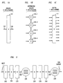
- FIGs. 1A-C illustrate and contrast respective analog, distributed analog and digital information representation and processing in accordance with one aspect of the present invention.
- a traditional single-wire 8-bit analog channel 101 is shown having a single input 102 and a single output 103.
- the circuit of FIG. 1A is contrasted with the 8-bit 8-channel (1-bit/channel) digital arrangement 111 of FIG. 1C.
- each input and each output represents a single bit.
- the illustrative distributed channel circuit of FIG. 1B is seen to comprise four communicating channels 120-1 through 120-4, each of which represents 2 bits/channel in accordance with one aspect of the present invention.
- channel should be understood to include (as appropriate for a given context) not only one or more transmission paths (e . g ., wires) for conveying continuous or discrete analog information and/or discrete digital signals, but also such storage, incrementing, coupling, rounding and other processing elements as may be used to combine, store and transfer computing primitives and signals.
- transmission paths e . g ., wires
- blocks 120-1 through 120-4 represent interacting low-precision analog processors. It will be appreciated that each of the low-precision analog processors will exhibit a precision of operations depending on the device characteristics and the nature of the signals to be processed.
- the incorporated Sarpeshkar paper provides further background on tradeoffs between computation and communication in choosing precision for analog channels.
- FIG. 2 illustrates periodic signal restoration via analog-digital-analog (A/D/A) conversion after a number of analog operations.
- the A/D/A behaves simply like an analog-to-digital converter followed by a digital-to-analog converter, though not necessarily implemented as such.
- A/D/A 225 functions to restore the analog signal appearing on lead 220 after analog operations by illustrative analog processors 205, 210 and 215 to one of a few discrete levels known as "attractor levels.”
- the number of attractor levels scales exponentially with the precision of the analog channels.
- the distance between attractor levels must be much greater (typically a few standard deviations depending on how high a bit error rate is tolerable) than the accumulated noise and offset between restoration stages.
- the signal restored to a discrete analog value at the output of A/D/A 225 is then illustratively processed by other analog processors (e . g ., processors 230, 235 and 240 in FIG. 2) before the output on analog path 245 is again restored by an A/D/A circuit 250 to produce the final output on single-wire path 260.
- the signal-restoration arrangement of FIG. 2 is a generalization of the 0-or-1 restoration scheme of typical prior art digital systems. Such digital systems typically require that the noise between stages be much less than the distance in voltage separation between the voltage for a '0' and that for a '1'.
- the optimal amount of analog processing that may be performed before a signal restoration is implemented will vary with application and is analyzed in the incorporated Sarpeshkar paper.
- Prior A/D/A circuits have been proposed for use as building blocks for certain storage and processing applications. See, for example, G. Cauwenberghs, "A Micropower CMOS Algorithmic A/D/A Converter, IEEE Transactions on Circuits and Systems I., Fundamental Theory and Applications, Vol . 42 (1995), No. 11, pp. 913-919. Such prior use did not extend, however, to use of A/D/A arrangements in hybrid systems as presently disclosed.
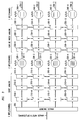
- FIG. 3 shows an illustrative system employing distributed analog processors and restoration of signals to discrete values after such processing. More specifically, an illustrative encoder 305 receives input on channel 300 from a source of 8-bit/channel information and encodes this information into four 2-bit/channel distributed analog processors. Encoder 305 will typically be an A/D converter, a bank-of-bandpass filters, or an electronic cochlea or retina. See C.A. Mead, Analog VLSI and Neural Systems , Addison-Wesley, Reading, MA, 1989, for illustrative electronic cochlea and retina circuits.
- This encoding cost incurred by encoder 305 in FIG. 3 is illustratively a purely analog computation whose costs are paid once at the front end of the system.
- the information output from encoder 305 is then processed in a distributed analog fashion, with illustrative interacting analog blocks 310-1 through 310-12, and is periodically restored via interacting A/D/A blocks 320-1 through 320-4.
- the outputs of A/D/A circuits 321-i are again applied to interconnected distributed analog processors, here 330-1, 4, 7, and 10 as shown in FIG. 3.
- the outputs of analog processors 330-3,6,9 and 12 are applied to respective A/D/A circuits 340-1 through 340-4 to again restore the processed signals to discrete levels on output leads 350-1 through 350-4.
- FIG. 3 illustrates by example the use of two different levels of precision in performing the level restorations in A/D/A circuits.
- restorations by A/D/A circuits are performed to a (relatively) fine level of precision (2 bits).
- the A/D/A operations by A/D/A circuits 350-1 through 350-4 are illustratively performed to 1-bit precision, as befits restorations of output signals of computations that compress information (e.g. decision making, pattern recognition etc.).
- analog processing blocks prior to the coarse restoration stages 340-i will tolerate a higher level of noise because of the greater separation of discrete levels.
- FIG. 5 shows illustrative capacitors 510 and 560 that serve to receive input charge. Each capacitor's state is advantageously changed by charging the capacitor with the sum of all its input currents ⁇ i I i . Unless otherwise mentioned, we will, for simplicity, also assume that all I i are positive, though no such restriction applies in the general case.
- the time period for integration of applied currents is taken as t in , a period that is conveniently gated by a pulse input, or is ungated.
- every analog state variable will likely reach the upper limit of its dynamic range, e . g ., the power supply voltage - or a fraction of the power supply voltage. It proves convenient in many contexts to prevent this from occurring, as will be appreciated from the following discussion, So, a threshold level of charge, Q T , is selected, such that if Q state ⁇ Q T , charging continues. But, if Q state > Q T , the state variable is reset to 0, and a signal is sent to a neighboring channel indicating that we have performed a reset; charging then resumes.
- the signal sent to the neighboring channel takes the form of a spike signal of the form described, e .
- the channel to which the illustrative spike signal is sent advantageously includes a similar charge-and-reset unit on another nearby capacitor. The spike then causes the neighboring channel to increment its charge by a discrete amount that is typically a fraction of Q T .
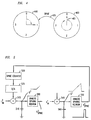
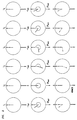
- FIG. 4 illustrates the charge-and-fire operation just described.
- a first circle 400 represents real numbers by their angular position of an arrow or vector 401 on the unit circle.
- the representation "wraps around” by resetting to 0, with the accompanying transmission of a (spike or other) signal 405 to the neighboring channel (represented by circle 410).
- the illustrative spike signal indicates that the preceding accumulate-and-fire circuit has caused the corresponding charge signal representation to perform one full revolution.
- the adjacent channel keeps track of the number of full revolutions performed at its neighbor circle 400, by a rotational increment at circle 410.
- the charge thus deposited on the capacitor corresponding to the angular displacement on circle 410 typically reflects a charge of less than Q T on that capacitor. This idea can be repeated ad infinitum , so that complete revolutions of the cited neighbor circle are accounted for by partial increments of yet another channel, and so on. It will be recognized that the approach just described overcomes limitations of the prior art regarding limited-dynamic-range for an analog variable.
- the above-described strategy represents information about a variable across many channels.
- One way of preserving the 2-bit representation across channels in is to increment the neighboring channel by ⁇ /2 whenever the current channel has finished a full revolution of 2 ⁇ .
- Such a scheme is illustrated in FIG. 5, where we charge the neighboring channel (the capacitor 510) by 1 unit when the current channel (capacitor 560) has completed a full revolution of 4 units.
- full revolutions of a neighbor result in a quarter-revolution increments of yet another neighbor to the left of it, and so on, a method is provided for approximating an analog number in a number representation based on radix 4.
- each of the channels of the described distributed number representation may also have its own analog input currents that arise from a source other than the immediate neighbor to their right.
- spiking outputs from spiking neuron circuit 550 reflecting a full charge on capacitor 560 (2 ⁇ rotation of its corresponding vector) are applied by connection to the neighboring channel to create an incremental charge on capacitor 510 for that neighboring channel vector
- the spiking signal from neuron circuit 550 advantageously is applied to current summer through a spike counter 520 and a (simple) digital-to-analog converter 525.
- an arriving spiking pulse can gate a standard charging current to the neighboring capacitor.
- This charging current may be chosen such that the charge is incremented by one unit.
- Such a scheme can be implemented using well-known circuit design techniques with as few as two transistors in series (one for gating and one for the current source). Any accumulated offsets due to mismatches in the current sources are irrelevant so long as we ensure that the sum of all these offsets is less than half the separation between discrete attractor levels prior to the roundoff operation.
- input currents I 2 / in other than the inter-channel spiking input from neuron circuit 550 are applied to charge a capacitor.
- the capacitor has received the threshold amount of charge (the capacitor has reached a corresponding threshold voltage) it fires a spike via a spiking neuron circuit.
- the inputs such as I 2 / in shown in FIG. 5 represent analog input currents to the respective channel for charging the respective channel capacitor to reflect signal conditions other than the spiking input from a neighboring channel.
- arbitrary logic and arithmetic functions can be performed on circuits based on the present inventive teachings as represented in simple form in FIG. 5.
- Performing an A/D conversion followed by a D/A conversion conveniently performs the A/D/A process used in the rounding operations described above and illustrated in FIGs. 2 and 3.
- a continuous variable is converted to its nearest discrete approximation, which is generally represented as a multi-bit binary number.
- a simple D/A converter then converts the binary number back to a continuous number to implement an A/D/A; the whole A/D/A process then performs a rounding operation.
- the incorporated patent application entitled Current-Mode Spike-Based Analog to Digital Conversion includes a number of figures and descriptions relating to the flow of operations in various analog-to-digital converter architectures.
- spikes illustratively cause transitions from one mode of operation with one configuration of neuronal charging currents to another mode of operation with another configuration of neuronal charging currents.
- the neuronal charging currents in turn generate spikes.
- flow diagrams are used in the design of a variety of useful functions, with analog-to-digital conversion being a good example.
- the following descriptions provide a formal method for characterizing a class of machines using these flow diagrams.
- the class of machines so described and characterized are conveniently referred to as hybrid state machines ( HSMs ).
- HSMs hybrid state machines
- hybrid state machines extend and expand the concept of finite state machines well known in digital computation.
- FIG. 6 An illustrative representation of a prior art finite state machine is shown in FIG. 6.
- a finite state machine is described by a flow diagram of discrete states, with transitions between discrete states always occurring in accordance with discrete clock cycles of a periodic clock (identified as Clk in FIG. 7).
- the inputs and outputs of the finite state machine are given by the binary vectors DI and DO respectively.
- the state of the machine is thus specified by the integer D .
- the transition to a next state depends only on the current state, and on the current value of the inputs. That is, to describe a finite state machine completely, we need only specify
- hybrid state machines possess both discrete digital states and continuous analog states, next-state functions for discrete and continuous states, analog and digital output functions, and interaction functions that define the interactions between the machine's analog and digital parts.
- no clock is required - all transitions are triggered by spiking events.
- Illustrative spiking circuits and signals are described in my incorporated patent application entitled Spiking Neuron Circuit . It will be appreciated that traditional finite-state machines are a special case of hybrid state machines with only digital inputs, with only discrete states, and with only one special input (the clock) that is capable of triggering transitions between states.
- FIG. 7 shows the architecture of an illustrative hybrid state machine.
- the machine is shown comprising two principal parts: (i) an analog part 720 with analog states AS (illustratively encoded on a set of capacitor charge variables), and with analog inputs and outputs AI and AO on leads 721 and 722, respectively; and (ii) a digital part 710 with discrete states DS encoded on a set of register variables stored in register 715 and having digital inputs and outputs DI and DO on leads 711 and 712, respectively.
- Analog part 720 also comprises analog processing element (s) 727, while digital part 710 further comprises combination logic 717.
- digital part 710 may alter the values of a set of binary outputs (binary control vector, 730) to control switches in the analog part 720, consequently affecting the analog system's operation.
- analog part 720 generates spiking events as an output spike vector, Sp , which triggers transitions between discrete states in digital part 710.
- Digital control of the analog part 720 of the hybrid state machine of FIG. 7 may be exercised in at least three ways.
- D/A converters DACs
- DACs D/A converters
- a current equal to 4 I 0 will illustratively be created by switching particular control bits supplied to a DAC to the bit pattern 100.
- This 4 I 0 current then changes the state of a capacitor in analog system 720 for which this current is a charging input.
- Any analog parameters such as thresholds, pulse widths, charging currents, capacitance values etc. may be altered this way.
- digital control bits alter the parameters of analog system 720 by setting selected analog parameters to zero while enabling other analog parameters to express their value.
- an analog input current, I in from outside the hybrid state machine may be allowed to assume its value during a sensing operation or it may be effectively set to zero, depending on the state of a specified control bit.
- digital control bits may reconfigure an analog topology by turning on or off particular switches included in analog processing unit 727 in analog portion 720. For example, an operational amplifier that is present in the analog system may be disconnected from the rest of the system when a particular digital control bit is 1.
- Control by analog part 720 of digital part 710 is effected by having particular spikes or particular spiking patterns trigger transitions between the discrete states.
- arbitrary spiking patterns may be recognized by a hybrid state machine that has all its transitions triggered by the arrival of a particular spike.
- the particular spike used to effect this transition may differ from state to state, but any given transition is always caused by one spike.
- This spike-pattern-recognition machine may be embedded within a larger hybrid state machine and have the spike-pattern-recognition machine generate a spike when the appropriate spiking pattern is recognized.
- all hybrid state machines make transitions based on only a single triggering spike.
- transitions between discrete states may be conditioned on a spike arrival as well as on the states of other digital inputs.
- the digital portion of a hybrid state machine (styled a spike-triggered finite state machine) is described in detail in my incorporated patent application filed on the same day entitled A Spike-Triggered Asynchronous Finite State Machine .
- Nonvolatile analog memory is difficult to realize in practice, we will generally assume that analog states are volatile and destructible, at least over a long time scale. Nonvolatile digital state is easily realized using such devices as SRAMs. Thus, if it is important to store analog state variables over a time scale that is much longer than the typical leak time of capacitors used in analog part 720, it will prove convenient to perform analog-to-digital conversion to the precision needed and store the analog state digitally. Such conversion may easily be performed using techniques described, e . g ., in my incorporated patent application Current-Mode Spike-Based Analog-to-Digital Conversion .
- a hybrid state machine for performing A/D conversion is readily embedded within a larger hybrid state machine.
- it proves convenient to transition from states of the larger machine to states of the conversion machine when we want to perform analog-to-digital conversion, and then return to the large machine when we complete the conversion.
- an analog-to-digital-conversion "subroutine" that we call from a larger (hybrid state machine) program. If we need to recreate some analog state on a capacitor, and this state has been stored digitally, we employ a standard digital-to- analog converter to charge the capacitor for a fixed amount of time with a current that represents the result of the digital-to-analog conversion.
- the storage and re-creation sequence for an analog state variable is an illustrative form of signal restoration implemented via the A/D/A technique described above in connection with FIGs. 2 and 3.
- A/D/A technique described above in connection with FIGs. 2 and 3.
- Certain changes in discrete states in digital part 710 of the hybrid state machine of FIG. 7 may result in no changes in analog part 720.
- A/D architectures e . g ., appearing in my incorporated patent application Current-Mode Spike-Based Analog-to-Digital Conversion
- counting spikes in a particular phase of A/D conversion alters the discrete states of a counter - but does not affect any analog parameters.
- Analog parameters advantageously change only after a transition to another phase of operation; such a transition is illustratively triggered by spikes that are not related to the spikes counted in the prior phase of operation.
- hybrid state machines As preamble, it proves advantageous to more formally define such a hybrid state machine.
- a hybrid state machine we need to specify its initial states, its next-state functions, its output functions, and its interaction functions that describe the interactions between its analog and digital parts.
- the digital inputs and outputs are given by the binary vectors DI and DO respectively
- the analog inputs and outputs are given by the real vectors AI and AO respectively
- the digital state is represented by the integer DS
- the analog state is represented by the vector AS (or, sometimes, QS )
- the spiking state variables are represented by the binary vector Sp
- the binary parameter vector C represents all the digital bits that control the analog part of the machine.
- FIG. 8 illustrates the state evolution for an illustrative winner-take-all computation in a hybrid state machine.
- a set of neurons each illustratively of the type shown in FIGs. 4 and 5, whose states have all been initialized at zero, receive respective currents corresponding to the input analog values.
- the largest input (I 2 ) causes its neuron to be the first to fire a spike, which spike is reported to the digital portion 710 of the hybrid machine of FIG. 7.
- This spike from the winning neuron causes a transition to a corresponding winning state that labels input I 2 to be the winner.
- the spike from the winning neuron may directly reset all non-winning inputs through interactions within the analog part of the state machine.
- This strategy seeks to avoid having other neurons develop into winners during the time needed to establish the first winner.
- the spike To perform direct reset during the transition, the spike must have a pulse width that is sufficiently long to accomplish a complete reset of the charge on a neuron.
- the spike-triggered finite state-machine 710 in FIG. 7 allows the machine to be in multiple discrete states simultaneously, thus allowing for multiple winners if the race is very close. Multiple winners may also arise because of mismatches in neuronal thresholds or capacitances.
- a winner may be disabled (but without resetting other neurons), thus permitting then-current losers to compete to determine a second-best neuron. If after the second best neuron is determined we disable its input (but not that of the other remaining neurons), we may obtain a third-best neuron. So, by repeating the procedure until all involved neurons are accounted for, we sort the input currents according to their values. When, at any stage of the process, there is more than one winner, all winners at that stage are disabled from competing in future stages.
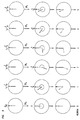
- FIG. 9 shows how we may use a hybrid state machine to recognize the direction of a vector, independent of its magnitude.
- N 5 in FIG. 9
- One of the neurons shown as neuron 0 in FIG. 9
- the other neurons are labeled from 1 to N , and perform computations on the N components of the vector.
- the current I 0 is such that it is greater than all other current components of the input vector I in , i . e ., I 0 > I i / in , for all i .
- the remaining N neurons are then charged with currents of I 0 - I i / in respectively.
- the other neurons have established positive residues proportional to I 0 - I i / in .
- the residue of the i th neuron is given by This means that the negative residues of the neurons, Q i / n , i .
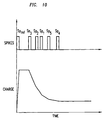
- FIG. 10 Curves relating to a method for measuring synchrony are illustrated in FIG. 10.
- a reference spike Sp ref causes a large burst of charge, Q mx , to build up on a capacitor.
- t pw is the pulse width of Sp ref .
- a spike Sp OR which is the logical OR of the spikes from neurons 1 to N .
- the capacitor holds its value, which is now a measure of synchrony amongst Sp l through Sp N .
- neuron i As soon as Sp i arrives, neuron i 's charging current is turned off to prevent the neuron from refiring.
- the capacitor on which the synchrony computation is performed may be the integration capacitor of another neuron; in that case, we must ensure that Q mx ⁇ Q T to prevent spiking.
- each spike contributes a penalty term in the summation that is in proportion to its distance from the first spike. If I lk is small compared with I 0 , then we do not penalize jitter much, and our pattern comparison between the stored weight vector and the input vector is forgiving. If I lk is large compared with I 0 , then we penalize jitter strongly, and our pattern comparison between the stored weight vector and the input vector is strict.
- FIG. 11 shows a building-block circuit that may be used to implement synchrony-measuring computations via simple logic.
- several such building-block circuits are connected together at a common V out node with global inputs V exc , V lk , Sp ref , and Sp frst that are the same across all spiking-input channels, and local inputs Sp i that differ from channel to channel.
- V exc global inputs
- V lk V lk
- Sp ref global inputs
- Sp frst that are the same across all spiking-input channels
- local inputs Sp i that differ from channel to channel.
- the voltage V exc enables us to control the amount of excitation charge dumped onto the synchrony output, marked V out in FIG. 11.
- Sp ref also serves to reset state variables on capacitors to initial values.
- the signal Sp frst corresponds to Sp OR
- the signal Sp i corresponds to the spiking input from neuron i .
- the voltage V lk controls the amount of leak current due to any spike.
- V lk may be different for different spikes if, e . g ., we want to weight certain components more heavily than others in our recognition. For example, components with greater variability in the data that are not as important for recognition may have slow leaks in the synchrony-measuring circuit while components with small variability in the data that are important for recognition may have fast leaks in the synchrony-measuring circuit.
- a solution that often proves optimum is to distribute the summation onto many capacitors and then add the final answers that accrue on these capacitors. Distributing the addition onto various capacitors is performed by having each capacitor get inputs from Sp ref to build up its excitation charge, from Sp OR to start the decay due to the first spike, and then have inputs from only the leak currents that correspond to the set of spikes that the capacitor is responsible for.
- the final addition of the residues on the capacitors after all spikes have arrived may be accomplished with hybrid state machines that perform addition of residues; these machines are described below.
- I 0 may be adapted via feed-forward circuits to be about twice that of the maximum value of Iin i . If I 0 is too much larger than the max. value of I i / in then the subtraction computation has to be done with great precision since we are subtracting very small numbers from a large number. If I 0 is Just a little larger than the maximum value of I i / in , then we risk getting a negative answer in the subtraction, due to offsets, which will result in zero current in our first-quadrant computations (only positive currents implies first-quadrant operation). Winner-take-all state machines based, e . g ., on the arrangement of FIG. 8 may be used to obtain the index i that corresponds to the maximum value of I i / in .
- a simple technique for adjusting the weight vectors is to use spike timing as a cue for learning. If we pick any arbitrary weight-vector from among the set of I i / w as a reference, then the spikes due to the other vectors will be early or late with respect to the spike fired by the reference vector.
- a spike-ordering circuit can detect the difference in spike timing and speed up or slow down the times of arrival of other spikes by adjusting their weight currents with respect to the reference Thus, if a spike is early, we reduce the weight current that produces this spike; if a spike is late we increase the weight current that produces the spike.
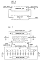
- FIG. 12A shows a circuit that detects the order between 2 spikes Sp 1 and Sp 2
- FIG. 12B shows a circuit that uses outputs from this circuit to perform adaptation.
- the voltages V p and V n are reset to V DD by an active low reference spike Sp ref (corresponding to Sp ref in FIG. 10) through transistors M11 and M12 respectively. These transistors are strong (have W / L's that are large, e . g ., 10 times larger) compared with the W / Ls of other transistors in the circuit), and are capable of overwhelming the positive-feedback state storage performed by M 7, M 9, and M 5 for V p , and by M8, M 10, and M6 for V n respectively.
- the positive feedback speeds up the response of the V p and V n voltages in the downward direction (towards ground), and helps store low values at either node - but is inactive in storing high values.
- FIG. 12B shows how the outputs of FIG. 12A may be used to perform adaptation.
- the voltages V TP and V TN set the time constants for upward and downward adaptation of the voltage V adpt respectively. Under normal operation, standard current-minor techniques would be used such that V TP and V TN are automatically adjusted to yield equal upward and downward rates of adaptation.
- V p is active (low)
- V adpt adapts in an upward direction through charging of the capacitor C .
- V n is active (low)
- V adpt adapts in a downward direction through discharging of the capacitor C.
- FIG. 12A and FIG. 12B implement a push-pull scheme for adapting V adpt in response to information about the order of spikes Sp 1 and Sp 2 .
- the voltage V adpt would in turn control a current that affects the spike order such that we have a closed feedback loop.
- an A/D quantization may be performed on this current to store its learned value digitally.
- the circuit of FIG. 11 also provides information about spike order, but in a more analog fashion. If Sp frst is replaced by Sp 1 , and Sp i by Sp 2 , then V out provides an analog measure of the difference in spike times between Sp 1 and Sp 2 , but only if Sp 1 occurs before Sp 2 . If we have another channel of the same circuit with the roles of Sp 1 and Sp 2 reversed, then we may obtain information about spike-time differences for both spike orderings. The difference in the output voltages of two such channels then yields a signed measure of the difference in spike times between Sp 1 and Sp 2 ; the difference may be utilized in a feedback loop to perform learning.
- Vector quantization is performed using the present inventive principles by performing a pattern match of an input vector to many stored weight vectors in parallel.
- the pattern matching is performed as described above, e . g ., in connection with FIG. 9.
- Application of the inventive pattern matching techniques generates score residues on capacitors, which are now designed to be parts of neuron circuits. The highest score residue corresponds to the best pattern match.
- the pattern-match scores for each vector may be distributed across many neurons as described above. In the latter case, we enact a first-to-spike race between a set of neurons, with each set composed of a few member neurons rather than just one neuron. All sets begin charging simultaneously with identical charging currents. Each set is charged according to a sequential procedure in which members of the set charge one at a time, fire a spike, shut themselves off and then permit the next member in the set to charge; when all members of the set have finished spiking, the set fires a spike. The earliest spike arrival from a set indicates that the best pattern match occurs for the vector associated with this set.
- Trellis vector quantization is an important technique for recognizing temporal sequences in speech. See, for example, B. Juan, "Design and performance of trellis vector quantizers for speech signals," IEEE Trans. Acoustics, Speech & Sig. Proc ., ASSP-36, 9: 1423-1431, Sept. 1988.
- a finite state machine transitions between states. In each state, vector quantization to a particular set of vectors is performed, which may change from state to state. The next-state transition function depends on the outcome of the current quantization as well as the current state.
- various temporal ordering constraints about a sequence of input vectors may be encoded in the structure of the finite state machine and in the set of quantization vectors in each state. It is also possible to construct pruning algorithms that train the machine from input data.
- Trellis vector quantization maps very naturally to an HSM architecture.
- the FSM of the quantizer is implemented by the spike-triggered FSM of the HSM.
- the weight vectors used for comparison are changed via a binary control vector that alters DAC input-bit information.
- First-spike information which encodes the best pattern match in each state may directly be used to trigger transitions to the next state. Learning is accomplished by spike-time adaptation algorithms as we have previously discussed.
- every spike in the timing pattern would require one neuron independent of whether it belonged to the same input or not. Recognizing timing patterns in spikes may be useful in feature-based speech recognition where each input spike signals the presence of a particular feature in speech ( e . g . a stop, silence, etc.). Learning timing patterns involves mechanisms of spike-time adaptation as discussed above.
- an HSM to generate any desired timing pattern of spikes by having discrete states with appropriate spike-triggering transitions and appropriate analog neuronal charging currents correspond to the inter-spike intervals in the pattern that we want to reproduce.
- Robots whether artificial or biological, often engage in discrete behaviors, e . g . swimming, running, walking, with each behavior having a smooth analog-dynamical-system description.
- the transitions from one behavior to the other are governed by events that occur in the world or inside the mind of the robot controller ( e . g . it gets tired).
- HSMs have a structure that is very similar - with a number of discrete states, within each of which the parameters of an analog dynamical system may be reconfigured. The transitions between discrete states occur by event-caused spikes.
- HSM's are well suited to the design of robot controllers.
- the control of aircraft involves hybrid control as well, with different controller configurations being used during takeoff, landing, cruising, banking etc.
- FSMs finite state machines
- HSMs hybrid state machines
- analog - Vector typically refers to an external vector of analog inputs (e . g . from a sensory array for smell), or to an internal vector ( e . g . from an on-chip filter-bank array used to decompose speech sounds from an external analog input).
- HSMs will consist of a spike-triggered FSM whose state transitions, states, and parameters in each state are be programmed using a general or special purpose language, and an analog special-purpose dynamical system suited to the task at hand.
- the analog part may involve resistive grids that perform image smoothing, or a filter bank for performing auditory processing.
- hybrid computation with spiking neurons and signal restoration naturally results in a distributed number representation.
- the radix depends on the precision to which we choose to maintain and restore analog information. It is then natural to perform digital arithmetic operations with these numbers. Because hybrid arithmetic operations are carried out in a higher radix than binary, there are fewer stages of processing when compared to normal binary processing, and fewer switching transitions, thus improving power and area efficiency. Furthermore, the use of analog primitives to perform basic arithmetic functions improves the power and area efficiency of implementing devices as well. A number of arithmetic processing techniques will now be described that exploit these and other advantages of hybrid computing.
- Counting is perhaps the most basic arithmetic operation.
- the computational question "Is the number of input pulses greater than 2 11 - 1?", may be answered in a purely digital, in a purely analog, and in a hybrid counter, as illustrated by FIGs. 13A-C.
- illustrative pulse counting is accomplished in the manner shown in FIG. 13A by having incoming pulses clock a 12-bit digital counter, and reading the result from a counter overflow signal at the MSB location.
- pulse counting is accomplished by having a neuron integrate impulses of charge that occur every time a spike is fired.
- the impulses of charge are advantageously chosen to be small enough that 2 12 impulses just cause the neuron to fire an overranging spike.
- the pulse-to-charge conversion may be accomplished via the excitatory synapse circuit shown in FIG. 14A, where the value of V wt determines the size of the charge events.
- FIG. 14B also shows an inhibitory synapse circuit capable of generating negative charge events as well.
- FIG. 13C shows a hybrid mode of counting in which 3 analog neurons interact with each other such that a sequence of 16 input charge events at any one neuron causes the generation of an overranging spike that is fed to its neighbor on the left.
- An overranging spike from the leftmost neuron in FIG. 13C signals that more than 2 11 - 1 spikes have arrived at the input.
- sub-threshold analog charge values are evaluated via the subranging analog-to-digital conversion techniques described in the incorporated patent application entitled Current-Mode Spike-Based Analog-to-Digital Conversion . Note that the hybrid counter may also be implemented in other configurations, e .
- non-integer powers of 2 may be used in the radix.
- a chief benefit of described hybrid schemes is that switching power dissipation is reduced because each stage switches less frequently than a binary stage. At the same time, large amounts of spatial or power resources are not spent in trying to maintain high precision in each hybrid stage. Thus many interacting moderate-precision analog processors can operate more efficiently than can purely analog or purely digital techniques. Analog feedback or calibration techniques may be used to improve the precision per hybrid stage. Since such techniques may operate on a very slow time scale or may be performed only occasionally, they yield little power overhead, although they do consume some device area.
- each pulse advantageously contributes an amount of charge such that when a pulse that causes overranging arrives, the pulse causes the charge accumulated on the neuron to slightly exceed the threshold of firing.
- the charge contribution per pulse must also be accurate enough such that the pulse that arrives before the one that causes overranging does not itself cause overranging.
- High-precision digital arithmetic e . g ., the addition of two 32-bit numbers
- the elementary adder units of digital arithmetic are logic circuits called full adders and half adders.
- Full adders take two 1-bit binary numbers A n and B n . and a 1-bit binary carry C n , and generate a local sum output S n and a carry output C n +l that is fed as an input to an adjacent higher-order channel.
- a half adder performs the same function as a full adder except that it does not accept a carry input C n .
- High-precision digital arithmetic may also be performed by present inventive hybrid computation techniques. This discussion focuses on how hybrid techniques may be used to add two 32-bit digital numbers. Other addition problems, e . g . how to add multiple numbers, is solved by a straightforward extension of the techniques used to solve this basic problem.
- the input bits are advantageously first grouped into moderate-precision chunks, typically 2-bit or 4-bit chunks. However, depending on the precision per channel in the hybrid technique any number of bits per chunk may be used.
- Each such chunk is converted to an analog current via a standard D/A operation.
- the analog currents are added through elementary analog operations described below.
- the interactions between channels are performed via overranging spike carries as illustrated in FIGS. 4 and 5, and pulse-to-charge synapses as illustrated, e . g ., in FIG. 14A and described below.
- the final answer on the various neuronal channels is read out by performing analog-to-digital conversion of the charge residues on each of the channels in parallel. Analog-to-digital conversion of charge residues is described in detail in my incorporated patent application entitled Current-Mode Spike-Based Analog-to-Digital Conversion .
- both charge residues may be positive and present on two neurons, N 1 and N 2 , and we may have no access to the input currents that created them.
- a timing neuron T to convert one of the residues to a negative one.
- the positive residue on N 1 is converted to a negative residue on T .
- Overranging spikes on neurons generate spikes which are fed to the adjacent channels as bursts of charge via a pulse-to-charge synapse as shown in FIGs. 4,5 and FIG. 14A.
- Such synapses are designed so that a full revolution of the channel generating the spike results in a 1/ r revolution of the channel receiving the spike, where r is the radix of the number representation.
- r is the radix of the number representation.
- Inactivating a spiking input may imply that charge is lost from this input for the portion of the time that the output spike overlaps the input spike in duration. To prevent this loss of charge, we must lengthen the pulse width of the input spike by the amount of overlap. Techniques for performing such operations and for compensating for even higher-order errors are discussed below.
- the addition is complete when all 16 channels have finished firing all of their timing spikes, and all output neurons have their spiking outputs at zero. In this situation, all carry propagations have terminated and the residues on the output neurons may be assumed to be correct. Thus, in the KCL case, the addition is complete when all timing neurons at all locations have fired a spike, and all the counting neurons have their outputs at zero. In the addition-of-residues case, the addition is complete when the timing neuron at all locations has finished firing a spike, the N 2 neuron at all locations has finished firing a spike, and all the N 1 neurons have their spiking outputs at zero. At this point, the residues on the output neurons may be used for further addition via an addition-of-residues technique, or we may perform sub-ranging analog-to-digital conversion on the output residues to obtain a final answer in digital format.
- a circuit for a hybrid state machine is easily constructed from its flow diagram, e . g ., the flow diagrams described above and in my incorporated patent application entitled Current-Mode Spike-Based Analog-to-Digital Conversion .
- Most of the circuit design may be accomplished by translating the description of the state machine into a circuit with the appropriate connectivity and logical interactions between and within building-block circuits.
- Three key building-block circuits in hybrid computation are a spiking neuron circuit, a toggle flip-flop and a spike-triggered finite state machine (FSM). Illustrative circuits of these respective kinds are described in the incorporated patent applications.
Landscapes
- Engineering & Computer Science (AREA)
- Physics & Mathematics (AREA)
- Theoretical Computer Science (AREA)
- Health & Medical Sciences (AREA)
- Life Sciences & Earth Sciences (AREA)
- Biomedical Technology (AREA)
- Biophysics (AREA)
- Evolutionary Computation (AREA)
- General Engineering & Computer Science (AREA)
- Data Mining & Analysis (AREA)
- Artificial Intelligence (AREA)
- General Health & Medical Sciences (AREA)
- Molecular Biology (AREA)
- Computing Systems (AREA)
- Computational Linguistics (AREA)
- General Physics & Mathematics (AREA)
- Mathematical Physics (AREA)
- Software Systems (AREA)
- Neurology (AREA)
- Control By Computers (AREA)
- Feedback Control In General (AREA)
- Analogue/Digital Conversion (AREA)
Applications Claiming Priority (2)
| Application Number | Priority Date | Filing Date | Title |
|---|---|---|---|
| US40753699A | 1999-09-29 | 1999-09-29 | |
| US407536 | 1999-09-29 |
Publications (2)
| Publication Number | Publication Date |
|---|---|
| EP1089221A2 true EP1089221A2 (de) | 2001-04-04 |
| EP1089221A3 EP1089221A3 (de) | 2007-05-02 |
Family
ID=23612491
Family Applications (1)
| Application Number | Title | Priority Date | Filing Date |
|---|---|---|---|
| EP00308088A Withdrawn EP1089221A3 (de) | 1999-09-29 | 2000-09-18 | Nadelimpulsbasierte hybride Datenverarbeitung |
Country Status (2)
| Country | Link |
|---|---|
| EP (1) | EP1089221A3 (de) |
| JP (1) | JP2001143011A (de) |
Cited By (8)
| Publication number | Priority date | Publication date | Assignee | Title |
|---|---|---|---|---|
| WO2004027680A1 (en) * | 2002-09-18 | 2004-04-01 | Canon Kabushiki Kaisha | Arithmetic circuit |
| US7533071B2 (en) | 2005-06-28 | 2009-05-12 | Neurosciences Research Foundation, Inc. | Neural modeling and brain-based devices using special purpose processor |
| US7610326B2 (en) | 2002-09-18 | 2009-10-27 | Canon Kabushiki Kaisha | Arithmetic circuit for calculating a cumulative value as a result of parallel arithmetic processing |
| US7627540B2 (en) | 2005-06-28 | 2009-12-01 | Neurosciences Research Foundation, Inc. | Addressing scheme for neural modeling and brain-based devices using special purpose processor |
| US7765029B2 (en) | 2005-09-13 | 2010-07-27 | Neurosciences Research Foundation, Inc. | Hybrid control device |
| US9104974B2 (en) | 2011-07-27 | 2015-08-11 | Samsung Electronics Co., Ltd. | Apparatus and method for transmitting and receiving determined spike events between neurons in neuromorphic chips utilizing a strobe representing spike occurrence time information |
| RU175095U1 (ru) * | 2015-01-12 | 2017-11-20 | федеральное государственное бюджетное образовательное учреждение высшего образования "Российский государственный гидрометеорологический университет" | Многофункциональный аналого-цифро-аналоговый элемент |
| WO2019211601A1 (en) * | 2018-04-30 | 2019-11-07 | Search For The Next Ltd | An analogue-digital hybrid computer |
Family Cites Families (1)
| Publication number | Priority date | Publication date | Assignee | Title |
|---|---|---|---|---|
| US3437800A (en) * | 1968-01-23 | 1969-04-08 | Hitachi Ltd | Synchronous and asychronous control for hybrid computer |
-
2000
- 2000-09-18 EP EP00308088A patent/EP1089221A3/de not_active Withdrawn
- 2000-09-27 JP JP2000293795A patent/JP2001143011A/ja active Pending
Cited By (12)
| Publication number | Priority date | Publication date | Assignee | Title |
|---|---|---|---|---|
| WO2004027680A1 (en) * | 2002-09-18 | 2004-04-01 | Canon Kabushiki Kaisha | Arithmetic circuit |
| US7610326B2 (en) | 2002-09-18 | 2009-10-27 | Canon Kabushiki Kaisha | Arithmetic circuit for calculating a cumulative value as a result of parallel arithmetic processing |
| US7533071B2 (en) | 2005-06-28 | 2009-05-12 | Neurosciences Research Foundation, Inc. | Neural modeling and brain-based devices using special purpose processor |
| US7627540B2 (en) | 2005-06-28 | 2009-12-01 | Neurosciences Research Foundation, Inc. | Addressing scheme for neural modeling and brain-based devices using special purpose processor |
| US8126828B2 (en) | 2005-06-28 | 2012-02-28 | Neuroscience Research Foundation, Inc. | Special purpose processor implementing a synthetic neural model of the human brain |
| US8326782B2 (en) | 2005-06-28 | 2012-12-04 | Neurosciences Research Foundation, Inc. | Addressing scheme for neural modeling and brain-based devices using special purpose processor |
| US7765029B2 (en) | 2005-09-13 | 2010-07-27 | Neurosciences Research Foundation, Inc. | Hybrid control device |
| US20120209432A1 (en) * | 2005-09-13 | 2012-08-16 | Neurosciences Research Foundation, Inc. | Hybrid control device |
| US8583286B2 (en) * | 2005-09-13 | 2013-11-12 | Neurosciences Research Foundation, Inc. | Hybrid control device |
| US9104974B2 (en) | 2011-07-27 | 2015-08-11 | Samsung Electronics Co., Ltd. | Apparatus and method for transmitting and receiving determined spike events between neurons in neuromorphic chips utilizing a strobe representing spike occurrence time information |
| RU175095U1 (ru) * | 2015-01-12 | 2017-11-20 | федеральное государственное бюджетное образовательное учреждение высшего образования "Российский государственный гидрометеорологический университет" | Многофункциональный аналого-цифро-аналоговый элемент |
| WO2019211601A1 (en) * | 2018-04-30 | 2019-11-07 | Search For The Next Ltd | An analogue-digital hybrid computer |
Also Published As
| Publication number | Publication date |
|---|---|
| EP1089221A3 (de) | 2007-05-02 |
| JP2001143011A (ja) | 2001-05-25 |
Similar Documents
| Publication | Publication Date | Title |
|---|---|---|
| US20220414025A1 (en) | System and methods for mixed-signal computing | |
| CN112445456B (zh) | 使用乘法器-累加器电路的系统、计算装置和方法 | |
| Dundar et al. | The effects of quantization on multilayer neural networks | |
| Shrestha et al. | In-hardware learning of multilayer spiking neural networks on a neuromorphic processor | |
| US20230359571A1 (en) | System and methods for mixed-signal computing | |
| KR20220086694A (ko) | 멤리스터 기반 신경 네트워크 트레이닝 방법 및 그 트레이닝 장치 | |
| US20220058492A1 (en) | Delta-sigma modulation neurons for high-precision training of memristive synapses in deep neural networks | |
| CN110288510B (zh) | 一种近传感器视觉感知处理芯片及物联网传感装置 | |
| EP1089436A2 (de) | Auf Nadelpulsen basierter Analog-Digital-Wandlung des Stromtyps | |
| KR101965850B1 (ko) | 인공 신경망에 사용되는 활성 함수의 확률적 구현 방법 및 그를 포함하는 시스템 | |
| Hasler | Opportunities in physical computing driven by analog realization | |
| TWI894388B (zh) | 用於分佈式多組件突觸計算結構之尖峰神經網路及方法 | |
| EP1089221A2 (de) | Nadelimpulsbasierte hybride Datenverarbeitung | |
| Fang et al. | An event-driven neuromorphic system with biologically plausible temporal dynamics | |
| Sarpeshkar et al. | Scalable hybrid computation with spikes | |
| US5140531A (en) | Analog neural nets supplied digital synapse signals on a bit-slice basis | |
| Yeo et al. | A power and area efficient CMOS stochastic neuron for neural networks employing resistive crossbar array | |
| JPH10134033A (ja) | コンボリューション操作を行うための電子装置 | |
| CN112734022A (zh) | 一种具有识别和排序功能的四字符忆阻神经网络电路 | |
| Zhao et al. | RACE-IT: A Reconfigurable Analog Computing Engine for In-Memory Transformer Acceleration | |
| Minai et al. | Disambiguation of pattern sequences with recurrent networks | |
| JPH04281584A (ja) | 複数の入力信号の重みづけられた複数の加算を行う装置 | |
| Craven | Inter-chip communications in an analogue neural network utilising frequency division multiplexing | |
| AbuHamra et al. | Memory-Centric Computing for Image Classification Using SNN with RRAM | |
| Rossmann et al. | short-and long-term dynamics in a stochastic pulse stream neuron implemented in FPGA |
Legal Events
| Date | Code | Title | Description |
|---|---|---|---|
| PUAI | Public reference made under article 153(3) epc to a published international application that has entered the european phase |
Free format text: ORIGINAL CODE: 0009012 |
|
| AK | Designated contracting states |
Kind code of ref document: A2 Designated state(s): AT BE CH CY DE DK ES FI FR GB GR IE IT LI LU MC NL PT SE |
|
| AX | Request for extension of the european patent |
Free format text: AL;LT;LV;MK;RO;SI |
|
| PUAL | Search report despatched |
Free format text: ORIGINAL CODE: 0009013 |
|
| AK | Designated contracting states |
Kind code of ref document: A3 Designated state(s): AT BE CH CY DE DK ES FI FR GB GR IE IT LI LU MC NL PT SE |
|
| AX | Request for extension of the european patent |
Extension state: AL LT LV MK RO SI |
|
| AKX | Designation fees paid | ||
| REG | Reference to a national code |
Ref country code: DE Ref legal event code: 8566 |
|
| STAA | Information on the status of an ep patent application or granted ep patent |
Free format text: STATUS: THE APPLICATION IS DEEMED TO BE WITHDRAWN |
|
| 18D | Application deemed to be withdrawn |
Effective date: 20071103 |