EP1087472A1 - Communication connector assembly with crosstalk compensation - Google Patents
Communication connector assembly with crosstalk compensation Download PDFInfo
- Publication number
- EP1087472A1 EP1087472A1 EP00307833A EP00307833A EP1087472A1 EP 1087472 A1 EP1087472 A1 EP 1087472A1 EP 00307833 A EP00307833 A EP 00307833A EP 00307833 A EP00307833 A EP 00307833A EP 1087472 A1 EP1087472 A1 EP 1087472A1
- Authority
- EP
- European Patent Office
- Prior art keywords
- contact wires
- connector
- board
- contact
- wire board
- Prior art date
- Legal status (The legal status is an assumption and is not a legal conclusion. Google has not performed a legal analysis and makes no representation as to the accuracy of the status listed.)
- Granted
Links
- 238000004891 communication Methods 0.000 title claims abstract description 19
- 230000013011 mating Effects 0.000 claims abstract description 20
- 230000008878 coupling Effects 0.000 description 12
- 238000010168 coupling process Methods 0.000 description 12
- 238000005859 coupling reaction Methods 0.000 description 12
- 230000001939 inductive effect Effects 0.000 description 8
- 239000004020 conductor Substances 0.000 description 4
- 238000005259 measurement Methods 0.000 description 4
- 239000000463 material Substances 0.000 description 3
- 230000005540 biological transmission Effects 0.000 description 2
- 229910000906 Bronze Inorganic materials 0.000 description 1
- RYGMFSIKBFXOCR-UHFFFAOYSA-N Copper Chemical compound [Cu] RYGMFSIKBFXOCR-UHFFFAOYSA-N 0.000 description 1
- 229910000881 Cu alloy Inorganic materials 0.000 description 1
- OAICVXFJPJFONN-UHFFFAOYSA-N Phosphorus Chemical compound [P] OAICVXFJPJFONN-UHFFFAOYSA-N 0.000 description 1
- 239000004676 acrylonitrile butadiene styrene Substances 0.000 description 1
- 230000000712 assembly Effects 0.000 description 1
- 238000000429 assembly Methods 0.000 description 1
- 230000009286 beneficial effect Effects 0.000 description 1
- DMFGNRRURHSENX-UHFFFAOYSA-N beryllium copper Chemical compound [Be].[Cu] DMFGNRRURHSENX-UHFFFAOYSA-N 0.000 description 1
- 239000010974 bronze Substances 0.000 description 1
- KUNSUQLRTQLHQQ-UHFFFAOYSA-N copper tin Chemical compound [Cu].[Sn] KUNSUQLRTQLHQQ-UHFFFAOYSA-N 0.000 description 1
- 230000000694 effects Effects 0.000 description 1
- 238000010292 electrical insulation Methods 0.000 description 1
- 238000009413 insulation Methods 0.000 description 1
- WABPQHHGFIMREM-UHFFFAOYSA-N lead(0) Chemical compound [Pb] WABPQHHGFIMREM-UHFFFAOYSA-N 0.000 description 1
- 238000000034 method Methods 0.000 description 1
- 239000000203 mixture Substances 0.000 description 1
- 238000012986 modification Methods 0.000 description 1
- 230000004048 modification Effects 0.000 description 1
- 239000004033 plastic Substances 0.000 description 1
- 229920003023 plastic Polymers 0.000 description 1
- 239000004417 polycarbonate Substances 0.000 description 1
- 229920000515 polycarbonate Polymers 0.000 description 1
- 239000000758 substrate Substances 0.000 description 1
- 238000003466 welding Methods 0.000 description 1
Images




Classifications
-
- H—ELECTRICITY
- H01—ELECTRIC ELEMENTS
- H01R—ELECTRICALLY-CONDUCTIVE CONNECTIONS; STRUCTURAL ASSOCIATIONS OF A PLURALITY OF MUTUALLY-INSULATED ELECTRICAL CONNECTING ELEMENTS; COUPLING DEVICES; CURRENT COLLECTORS
- H01R13/00—Details of coupling devices of the kinds covered by groups H01R12/70 or H01R24/00 - H01R33/00
- H01R13/646—Details of coupling devices of the kinds covered by groups H01R12/70 or H01R24/00 - H01R33/00 specially adapted for high-frequency, e.g. structures providing an impedance match or phase match
- H01R13/6461—Means for preventing cross-talk
- H01R13/6467—Means for preventing cross-talk by cross-over of signal conductors
-
- Y—GENERAL TAGGING OF NEW TECHNOLOGICAL DEVELOPMENTS; GENERAL TAGGING OF CROSS-SECTIONAL TECHNOLOGIES SPANNING OVER SEVERAL SECTIONS OF THE IPC; TECHNICAL SUBJECTS COVERED BY FORMER USPC CROSS-REFERENCE ART COLLECTIONS [XRACs] AND DIGESTS
- Y10—TECHNICAL SUBJECTS COVERED BY FORMER USPC
- Y10S—TECHNICAL SUBJECTS COVERED BY FORMER USPC CROSS-REFERENCE ART COLLECTIONS [XRACs] AND DIGESTS
- Y10S439/00—Electrical connectors
- Y10S439/941—Crosstalk suppression
Definitions
- This invention relates to communication connectors that are configured to compensate for crosstalk produced between different signal paths through the connector.
- crosstalk occurs when signals conducted over a first signal path, e.g., a pair of terminal contact wires associated with a communication connector, are partly transferred by inductive or capacitive coupling into a second signal path, e.g., another pair of terminal contact wires in the same connector.
- the transferred signals define "crosstalk" in the second signal path, and such crosstalk degrades any signals that are being routed over the second path.
- an industry type RJ-45 communication connector typically includes four pairs of terminal wires defining four different signal paths.
- all four pairs of terminal wires extend closely parallel to one another over the lengths of the connector bodies.
- signal crosstalk may be induced between and among different pairs of terminal wires, particularly in a mated RJ-45 plug and jack combination. The amplitude of the crosstalk becomes stronger as the coupled signal frequencies or data rates increase.
- NEXT near-end crosstalk
- U.S. Patent 5,186,647 to Denkmann, et al (Feb. 16, 1993), which is assigned to the assignee of the present invention and application, discloses an electrical connector with crosstalk compensation for conducting high frequency signals.
- the connector has a pair of metallic lead frames mounted flush with a dielectric spring block, with connector terminals formed at opposite ends of the lead frames.
- the lead frames themselves include flat elongated conductors each of which includes a spring terminal contact wire at one end for contacting a corresponding terminal of a mating connector, and an insulation displacing connector (IDC) terminal at the other end for connection with an outside insulated wire lead.
- IDC insulation displacing connector
- the lead frames are placed one over the other on the spring block, and three conductors of one lead frame have cross-over sections formed to overlap corresponding cross-over sections formed in three conductors of the other lead frame. All relevant portions of the '647 patent are incorporated by reference herein.
- U.S. Patent 5,580,270 (Dec. 3, 1996) also discloses an electrical plug connector having crossed pairs of contact strips.
- Crosstalk compensation circuitry may also be provided on or within layers of a printed wire board, to which spring terminal contact wires of a communication jack are connected within the jack housing.
- the terminal contact wires have base portions that enter a wire board alternatingly along two rows which are perpendicular to the direction of the contact wires, thus defining a staggered wire board entry pattern or "footprint". Coupling of a polarity opposite to that needed for crosstalk compensation may be introduced among the base portions of the contact wires, however, and the amount of crosstalk compensation needed elsewhere (e.g., on the wire board) to achieve Category 6 performance may need to be increased as a result.
- a so-called "MAX 6" modular jack outlet available from The Siemon Company has a printed wire board and four pairs of contact wires that extend generally normal to the board. No cross-over is formed in any of the wire pairs, and the contact wires enter the wire board along three rows.
- a communication jack connector which, when mated with a typical RJ-45 plug, provides such crosstalk compensation that the mated connectors will meet or exceed the proposed Category 6 performance levels, is highly desirable.
- a communication connector assembly includes a wire board, and a number of elongated terminal contact wires that extend in a generally horizontal direction with respect to a top surface of the wire board.
- Each of the contact wires has a free end portion for making electrical contact with a mating connector, the latter acting to introduce offending crosstalk from a line of contact with the contact wires over a first region of the wires.
- a base portion opposite the free end portion is formed to connect each contact wire to the wire board, and the base portion projects in a generally normal direction with respect to the top surface of the board.
- At least one pair of adjacent contact wires has a cross-over section that demarcates a second region in which generally horizontal portions of the contact wires are coupled for crosstalk compensation.
- the base portions of the contact wires enter the wire board with an entry pattern that is dimensioned and arranged to produce a third region in which the base portions are also coupled for crosstalk compensation.
- FIG. 1 is a perspective view of a first embodiment of a communication connector assembly 10, and a communications jack frame or housing 12 with which the assembly 10 is associated.
- the jack housing 12 has a front face in which a plug opening 13 is formed.
- the plug opening 13 has an axis P along the direction of which a mating plug connector may be inserted in the jack housing 12.
- FIG. 2 is an enlarged, perspective view of a wire board portion of the connector assembly 10 in FIG. 1.
- the communication connector assembly 10 includes a generally rectangular printed wire board 14.
- the board 14 may be in the form of, e.g., a single or a multi-layer dielectric substrate.
- a number, e.g., eight elongated terminal contact wires 18a-18h extend in a generally horizontal direction with respect to a top surface of the wire board 14, substantially parallel to one another.
- the contact wires are generally uniformly spaced a certain distance (e.g., 0.090 inches) from the top surface of the wire board 14, and free end portions of the contact wires project beyond a front edge 19 of the board.
- the contact wires 18a-18h are also configured to deflect resiliently toward the board 14 when the wires are engaged by a mating connector along the direction of the plug opening axis P, i.e., in a direction parallel to the wire board 14.
- the terminal contact wires 18a-18h may be formed from, e.g., a copper alloy such as spring-tempered phosphor bronze, beryllium copper, or the like.
- a typical cross-section for the contact wires 18a-18h is approximately 0.015 inches square.
- the board 14 may incorporate electrical circuit components and devices arranged to compensate for connector-induced crosstalk. Such devices may include wire traces printed on or within layers of the board 14, as disclosed in the mentioned '741 application. Crosstalk compensation provided by the board 14 may be in addition to an initial, stage of crosstalk compensation provided by the terminal contact wires 18a-18h, as explained below.
- the terminal contact wires 18a-18h have associated base portions 20a-20h opposite their free end portions (see FIG. 2). Each base portion is formed to connect a contact wire to one or more conductors on or within the wire board 14.
- the base portions 20a-20h may be soldered or press-fit in plated terminal openings formed through the board, to connect with corresponding conductive paths on or within the board.
- the base portions 20a-20h project in a generally normal direction with respect to the top surface of the wire board 14 (see FIG. 3).
- the base portions 20a-20h enter the wire board 14 with a "duo diagonal " footprint, described below in connection with FIG. 4.
- the base portions of the terminal contact wires enter the wire board with a "saw tooth” footprint which is also described below in connection with FIGS. 5 and 6.
- An electrically insulative, dielectric terminal housing 50 (FIG. 1) covers a rear portion of the wire board 14. Outside insulated wire leads may be connected to upstanding terminals 56a to 56h on the board which terminals are only partly surrounded by housing terminal guards.
- the housing 50 is formed of a plastics or other insulative material that meets all applicable standards with respect to electrical insulation and flammability. Such materials include but are not limited to polycarbonate, ABS, and blends thereof.
- the housing 50 has, for example, at least one fastening or mounting post (not shown) that projects from a bottom surface of the housing to pass through one or more openings 58 in the board 14.
- Terminals 56a-56h are mounted at opposite sides of the rear portion of the wire board 14, as seen in FIGS. 1 and 2. Each of the terminals 56a-56h has a mounting portion that is soldered or press fit in a corresponding terminal mounting hole in board 14, to connect via a conductive path (not shown) with a corresponding one of the terminal contact wires 18a-18h.
- the fastening post of the housing 50 aligns with the opening 58 in the board 14, and passes through to project below the board.
- a cover 60 is formed of the same or a similar material as that of the terminal housing 50.
- the cover 60 is arranged to protect the rear portion of the wire board from below.
- Cover 60 has at least one opening 62 which aligns with the tip of the fastening post of housing 50 below the wire board 14.
- the board 14 is thus secured between the terminal housing 50 and the cover 60, and a tip of the housing fastening post or posts are joined to the body of the cover 60.
- a known ultrasonic welding process may be used to melt and fuse the post tip and the surrounding cover body with one another. With the wire board 14 thus captured between the terminal housing 50 and the cover 60, the rear portion of the wire board is protectively enclosed. See U.S. Patent 5,924,896 issued July 20, 1999, and assigned to the assignee of the present invention and application. All relevant portions of the '896 patent are incorporated by reference herein.
- the free end portions of the terminal contact wires 18a-18h are formed to make electrical contact with corresponding contact wires of a mating plug connector 88 (see FIG. 3).
- a line of contact 72 is defined transversely of the contact wires, along which the contact wires make electrical contact with corresponding terminals of the plug connector 88.
- the contact wires 18a-18h are engaged by the mating plug connector 88 in the direction of the plug opening axis P, their free end portions deflect in unison in the direction of the board 14 as shown in FIG. 3.
- different pairs of the eight terminal contact wires 18a-18h are numbered and identified as follows, with reference to FIGS. 4 and 5.
- Contact wire pair nos. 1, 2 and 4 have cross-over sections 74 at which each contact wire of a given pair is stepped toward and crosses over the other contact wire of the pair, with a generally "S"-shaped side-wise step 76.
- the terminal contact wires curve arcuately above and below their common plane at each cross-over section 74, as seen in FIGS. 2 and 3.
- Opposing faces of the step 76 in the contact wires are spaced typically by about 0.035 inches (i.e., enough to prevent shorting when the terminal wires are engaged by a mating connector).
- the cross-over sections 74 are formed on pairs 1, 2 and 4, i.e., contact wires 18d & 18e; 18a & 18b; and 18g & 18h.
- the "pair 3" contact wires (18c and 18f) straddle either side of contact wire pair no. 1 (wires 18d and 18e), and no cross-over section is associated with the "pair 3" contact wires 18c, 18f. That is, contact wires 18c and 18f extend without a side-wise step, and pairs of contact wires that have the cross-over sections are adjacent either side of the "pair 3" contact wires 18c & 18f.
- the cross-over sections 74 are relatively close to the line of contact 72. Thus, crosstalk compensation by the connector assembly 10 begins to operate near the line of contact 72, beginning with the cross-over sections 74 whose centers may be located, for example, approximately 0.148 inches from the line of contact 72.
- FIGS. 1 - 3 also show a terminal wire guide block 78 mounted over the front edge 19 of the wire board 14.
- the guide block 78 has equi-spaced vertical guide ways 86.
- the free end portions of the terminal contact wires are arranged to extend within corresponding ones of guide ways 86, and to be guided individually for vertical movement when deflected by the terminals of the mating plug connector 88 as in FIG. 3.
- the wire board 14 with the terminal contact wires 18a-18h projecting from its front edge 19, is inserted in a passage 89 that opens in a rear wall of the jack housing 12.
- Side edges of the board 14 may be guided for entry into the housing 12 by, e.g., flanges that project inwardly from side walls of the jack housing 12.
- the jack housing has a slotted catch bar 90 protruding horizontally off of a bottom wall 91 of the housing.
- the bar 90 is arranged to receive and to hold a flange 92 (FIG. 1) that projects downward beneath the wire board cover 60, and the wire board 14 is thus fixed securely in an operative position inside the jack housing.
- the surface of the wire board 14 is parallel to the plug opening axis P, along the direction of which the plug connector 88 engages and disengages the free end portions of the contact wires 18a-18h.
- the connector assembly 10 produces predominantly inductive crosstalk compensation coupling among co-planar portions of the terminal contact wires 18a-18h, beyond the cross-over sections 74, in such a manner as to create an initial stage of crosstalk compensation.
- This initial stage opposes or compensates for crosstalk introduced when the free end portions of the contact wires operatively engage the terminals of the plug connector 88.
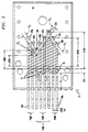
- FIG. 4 is a plan view of the connector assembly 10, wherein the base portions 20a-20h enter the wire board 14 with a duo-diagonal footprint pattern. Measurements shown on the drawing are typical dimensions in inches, and are not intended to limit the invention with respect to any particular dimension or sets of dimensions.
- the points of entry of the base portions define four rows on the wire board 14, which rows are substantially perpendicular to the long direction of the terminal contact wires 18a-18h. The points of entry also define two successive diagonal lines through the rows.
- Region A 1 corresponds to a zone in which offending crosstalk is introduced by a mating connector. Since region A 1 begins with the line of contact 72, and ends at the center of the cross-over sections 74, the horizontal distance of region A 1 is kept as short as possible, e.g., about 0.148 inches in FIG. 4. Here, a short distance minimizes transmission delay and reduces the overall amount of inductive and capacitive compensation required of the connector assembly 10 to counter the effects of the offending crosstalk.
- the points of entry of the base portions define four rows on the wire board 14, which rows are substantially perpendicular to the long direction of the terminal contact wires 18a-18h. The points of entry also define two successive diagonal lines through the rows.
- Region A 2 defines a zone in which portions of the contact wires 18a-18h are horizontal and coplanar with one another between the cross-over sections 74 and the base portions 20a-20h, with a substantially uniform spacing (e.g., about .090 inches) above the board surface. See FIG. 3. Sides of adjacent contact terminal wires are spaced apart typically by about 0.025 inches in region A 2 , and inductive and capacitive compensation coupling is very effective among the contact wires.
- Region A 3 in FIG. 4 represents a zone where the contact wires bend and the base portions 20a-20h extend generally normally of the wire board 14 to enter terminal openings in the board.
- centers of adjacent base portions are spaced typically by about 0.060 inches in the long direction of the contact wires, i.e., by a spacing greater than the typical 0.040 inch center-to-center spacing of the contact wires at their line of contact 72 with a mating connector.
- the region A 3 includes adjacent base portions which are substantially parallel and co-planar with one another in a direction normal to the wire board 14. Inductive as well as capacitive crosstalk compensation coupling will therefore be produced among the base portions in region A 3 , when the adjacent base portions are ordered as shown in FIG. 4 and described below.
- FIG. 5 is a plan view of the connector assembly 10, wherein the base portions 20a-20h of the terminal contact wires enter the wire board 14 with a foot print pattern resembling a coarse saw tooth.
- FIG. 6 is a perspective view of the wire board 14 in FIG. 5. The points of entry of the base portions define four rows on the wire board 14, which rows are sustantially perpendicular to the long direction of the contact wires. The entry pattern also forms a saw tooth running through the rows.
- the length of region A 1 in the direction of the contact wires is kept relatively short (e.g., about 0.148 inches) to minimize transmission delay and to reduce the amount of inductive and capacitive compensation needed to counter the offending crosstalk.
- Region A 2 in FIG. 5 depicts an effective inductive and capacitive coupling zone among horizontal portions of the terminal contact wires 18a-18h.
- the contact wires lie in substantially the same plane and are horizontal with respect to the surface of the wire board 14, with a substantially uniform spacing (e.g., 0.090 inches ⁇ above the surface of the board 14.
- a substantially uniform spacing e.g., 0.090 inches ⁇ above the surface of the board 14.
- Region A 3 in FIG. 5 represents a zone where the contact wires bend and the base portions 20a-20h extend generally normal to the wire board 14, to enter terminal openings in the board. Adjacent base portions in region A 3 are spaced apart typically by about 0.060 inches in the long direction of the contact wires, i.e., by a spacing greater than the typical 0.040 inch spacing between centers of the contact wires at their line of contact 72 with a mating connector.
- the region A 3 comprises adjacent base portions which are substantially parallel and co-planar with one another in a direction normal to the wire board 14. Inductive and capacitive crosstalk compensation coupling is produced among the base portions in region A 3 , when the adjacent base portions are ordered as shown in FIG. 5 and described below.
- contact wire 18d of pair 1 is adjacent to contact wire 18c of pair 3.
- a relation that contributes effectively to crosstalk compensation is one that positions base portion 20e of pair 1 closer to base portion 20c of pair 3, and base portion 20d of pair 1 further from base portion 20c of pair 3.
- base portion 20d of pair 1 is positioned closer to base portion 20f of pair 3, while base portion 20e of pair 1 is placed further from base portion 20f of pair 3.
- the configurations in either of FIGS. 4 or 5 satisfy such relationships.
- terminal contact wire 18c of pair 3 is adjacent to wire 18b of pair 2.
- a relation that contributes effectively to crosstalk compensation is one that brings base portion 20c of pair 3 closer to base portion 20a of pair 2, and base portion 20c of pair 3 further from base portion 20b of pair 2.
- base portion 20c is adjacent to base portion 20a in the region A 3
- base portion 20b is separated from base portion 20c by the base portion 20a in region A 3 .
- the entry patterns for base portions 20d, 20e of pair 1, and 20a, 20b of pair 2 in FIGS. 4 and 5, are such that the sum of (a) the distance between base portions 20a and 20d, and (b) the distance between base portions 20b and 20e; minus the sum of (c) the distance between base portions 20a and 20e, and (d) the distance between base portions 20b and 20d, is minimized.
- Such a relation tends to minimize the amount of any offending crosstalk introduced by the base portions.
- FIGS. 7 and 8 are tables showing NEXT measurement results when using the duo-diagonal entry pattern of the contact wire base portions 20a-20h, as in FIGS. 1-4, and with additional compensation within the wire board 14.
- Category 6 performance was obtained in both forward (FIG. 7) and reverse (FIG. 8) crosstalk measurements.
Landscapes
- Coupling Device And Connection With Printed Circuit (AREA)
- Details Of Connecting Devices For Male And Female Coupling (AREA)
Abstract
Description
- This invention relates to communication connectors that are configured to compensate for crosstalk produced between different signal paths through the connector.
- There is a need for a durable, high-frequency communication connector assembly that compensates for (i.e., cancels or reduces) crosstalk produced between different signal paths carried through the connector. As defined herein, crosstalk occurs when signals conducted over a first signal path,e.g., a pair of terminal contact wires associated with a communication connector, are partly transferred by inductive or capacitive coupling into a second signal path, e.g., another pair of terminal contact wires in the same connector. The transferred signals define "crosstalk" in the second signal path, and such crosstalk degrades any signals that are being routed over the second path.
- For example, an industry type RJ-45 communication connector typically includes four pairs of terminal wires defining four different signal paths. In the conventional RJ-45 plug and jack connectors, all four pairs of terminal wires extend closely parallel to one another over the lengths of the connector bodies. Thus, signal crosstalk may be induced between and among different pairs of terminal wires, particularly in a mated RJ-45 plug and jack combination. The amplitude of the crosstalk becomes stronger as the coupled signal frequencies or data rates increase.
- Applicable industry standards for rating the degree to which communication connectors exhibit crosstalk, do so in terms of near-end crosstalk or "NEXT". Moreover, NEXT ratings are typically specified for mated plug and jack combinations, wherein the input terminals of the plug connector are used as a reference plane. Communication links using unshielded twisted pairs (UTP) of copper wire are now expected to support data rates up to not only 100 MHz or industry standard "Category 5" performance, but to meet proposed "
Category 6" performance levels which call for at least 46 dB crosstalk loss at 250 MHz. - U.S. Patent 5,186,647 to Denkmann, et al (Feb. 16, 1993), which is assigned to the assignee of the present invention and application, discloses an electrical connector with crosstalk compensation for conducting high frequency signals. The connector has a pair of metallic lead frames mounted flush with a dielectric spring block, with connector terminals formed at opposite ends of the lead frames. The lead frames themselves include flat elongated conductors each of which includes a spring terminal contact wire at one end for contacting a corresponding terminal of a mating connector, and an insulation displacing connector (IDC) terminal at the other end for connection with an outside insulated wire lead. The lead frames are placed one over the other on the spring block, and three conductors of one lead frame have cross-over sections formed to overlap corresponding cross-over sections formed in three conductors of the other lead frame. All relevant portions of the '647 patent are incorporated by reference herein. U.S. Patent 5,580,270 (Dec. 3, 1996) also discloses an electrical plug connector having crossed pairs of contact strips.
- Crosstalk compensation circuitry may also be provided on or within layers of a printed wire board, to which spring terminal contact wires of a communication jack are connected within the jack housing. See U.S. Patent Application No. 08/923,741 filed September 29, 1997, and assigned to the assignee of the present application and invention. All relevant portions of the '741 application are incorporated by reference herein. See also U.S. Patent 5,299,956 (Apr. 5, 1994).
- U.S. Patent Application No. 09/264,506 filed March 8, 1999, and assigned to the assignee of the present invention and application, discloses a communication connector assembly having generally co-planar terminal contact wires. Certain pairs of the contact wires have opposed cross-over sections near their line of contact with a mating connector, and a coupling region along the wires beyond the cross-over sections compensates for crosstalk introduced by the mating connector. All relevant portions of the '506 application are also incorporated by reference herein.
- In the connector assembly of the above '506 application, the terminal contact wires have base portions that enter a wire board alternatingly along two rows which are perpendicular to the direction of the contact wires, thus defining a staggered wire board entry pattern or "footprint". Coupling of a polarity opposite to that needed for crosstalk compensation may be introduced among the base portions of the contact wires, however, and the amount of crosstalk compensation needed elsewhere (e.g., on the wire board) to achieve
Category 6 performance may need to be increased as a result. - A so-called "MAX 6" modular jack outlet available from The Siemon Company has a printed wire board and four pairs of contact wires that extend generally normal to the board. No cross-over is formed in any of the wire pairs, and the contact wires enter the wire board along three rows.
- A communication jack connector which, when mated with a typical RJ-45 plug, provides such crosstalk compensation that the mated connectors will meet or exceed the proposed
Category 6 performance levels, is highly desirable. - According to the invention, a communication connector assembly includes a wire board, and a number of elongated terminal contact wires that extend in a generally horizontal direction with respect to a top surface of the wire board. Each of the contact wires has a free end portion for making electrical contact with a mating connector, the latter acting to introduce offending crosstalk from a line of contact with the contact wires over a first region of the wires. A base portion opposite the free end portion is formed to connect each contact wire to the wire board, and the base portion projects in a generally normal direction with respect to the top surface of the board. At least one pair of adjacent contact wires has a cross-over section that demarcates a second region in which generally horizontal portions of the contact wires are coupled for crosstalk compensation. The base portions of the contact wires enter the wire board with an entry pattern that is dimensioned and arranged to produce a third region in which the base portions are also coupled for crosstalk compensation.
- For a better understanding of the invention, reference is made to the following description taken in conjunction with the accompanying drawing, and the scope of the invention will be pointed out by the appended claims.
- In the drawing:
- FIG. 1 is a perspective view of a first embodiment of a communication connector assembly according to the invention;
- FIG. 2 is an enlarged, perspective view of a wire board portion of the connector assembly in FIG. 1;
- FIG. 3 is a side view of the wire board portion as seen from the right in FIG. 2, with the wire board portion inserted in a jack frame;
- FIG. 4 is a plan view of the wire board portion in FIG. 2;
- FIG. 5 is a plan view of a second embodiment of the wire board portion of the connector assembly in FIG. 1;
- FIG. 6 is a perspective view of the wire board portion in FIG. 5; and
- FIGS. 7 and 8 are tables showing measurement
results meeting Category 6 levels with the embodiment of FIGS. 1 - 4. -
- FIG. 1 is a perspective view of a first embodiment of a
communication connector assembly 10, and a communications jack frame orhousing 12 with which theassembly 10 is associated. Thejack housing 12 has a front face in which a plug opening 13 is formed. The plug opening 13 has an axis P along the direction of which a mating plug connector may be inserted in thejack housing 12. FIG. 2 is an enlarged, perspective view of a wire board portion of theconnector assembly 10 in FIG. 1. - In the illustrated embodiment, the
communication connector assembly 10 includes a generally rectangular printedwire board 14. Theboard 14 may be in the form of, e.g., a single or a multi-layer dielectric substrate. A number, e.g., eight elongatedterminal contact wires 18a-18h extend in a generally horizontal direction with respect to a top surface of thewire board 14, substantially parallel to one another. The contact wires are generally uniformly spaced a certain distance (e.g., 0.090 inches) from the top surface of thewire board 14, and free end portions of the contact wires project beyond afront edge 19 of the board. Thecontact wires 18a-18h are also configured to deflect resiliently toward theboard 14 when the wires are engaged by a mating connector along the direction of the plug opening axis P, i.e., in a direction parallel to thewire board 14. - The
terminal contact wires 18a-18h may be formed from, e.g., a copper alloy such as spring-tempered phosphor bronze, beryllium copper, or the like. A typical cross-section for thecontact wires 18a-18h is approximately 0.015 inches square. - The
board 14 may incorporate electrical circuit components and devices arranged to compensate for connector-induced crosstalk. Such devices may include wire traces printed on or within layers of theboard 14, as disclosed in the mentioned '741 application. Crosstalk compensation provided by theboard 14 may be in addition to an initial, stage of crosstalk compensation provided by theterminal contact wires 18a-18h, as explained below. - The
terminal contact wires 18a-18h have associatedbase portions 20a-20h opposite their free end portions (see FIG. 2). Each base portion is formed to connect a contact wire to one or more conductors on or within thewire board 14. For example, thebase portions 20a-20h may be soldered or press-fit in plated terminal openings formed through the board, to connect with corresponding conductive paths on or within the board. Thebase portions 20a-20h project in a generally normal direction with respect to the top surface of the wire board 14 (see FIG. 3). - In the embodiment of FIG. 2, the
base portions 20a-20h enter thewire board 14 with a "duo diagonal" footprint, described below in connection with FIG. 4. In a second embodiment of theconnector assembly 10, the base portions of the terminal contact wires enter the wire board with a "saw tooth" footprint which is also described below in connection with FIGS. 5 and 6. - An electrically insulative, dielectric terminal housing 50 (FIG. 1) covers a rear portion of the
wire board 14. Outside insulated wire leads may be connected toupstanding terminals 56a to 56h on the board which terminals are only partly surrounded by housing terminal guards. Thehousing 50 is formed of a plastics or other insulative material that meets all applicable standards with respect to electrical insulation and flammability. Such materials include but are not limited to polycarbonate, ABS, and blends thereof. Thehousing 50 has, for example, at least one fastening or mounting post (not shown) that projects from a bottom surface of the housing to pass through one ormore openings 58 in theboard 14. -
Terminals 56a-56h are mounted at opposite sides of the rear portion of thewire board 14, as seen in FIGS. 1 and 2. Each of theterminals 56a-56h has a mounting portion that is soldered or press fit in a corresponding terminal mounting hole inboard 14, to connect via a conductive path (not shown) with a corresponding one of theterminal contact wires 18a-18h. When theterminal housing 50 is aligned above theIDC terminals 56a-56h, and thehousing 50 is lowered to receive the IDC terminals in corresponding slots in the terminal guards, the fastening post of thehousing 50 aligns with theopening 58 in theboard 14, and passes through to project below the board. - A
cover 60 is formed of the same or a similar material as that of theterminal housing 50. Thecover 60 is arranged to protect the rear portion of the wire board from below.Cover 60 has at least oneopening 62 which aligns with the tip of the fastening post ofhousing 50 below thewire board 14. Theboard 14 is thus secured between theterminal housing 50 and thecover 60, and a tip of the housing fastening post or posts are joined to the body of thecover 60. For example, a known ultrasonic welding process may be used to melt and fuse the post tip and the surrounding cover body with one another. With thewire board 14 thus captured between theterminal housing 50 and thecover 60, the rear portion of the wire board is protectively enclosed. See U.S. Patent 5,924,896 issued July 20, 1999, and assigned to the assignee of the present invention and application. All relevant portions of the '896 patent are incorporated by reference herein. - The free end portions of the
terminal contact wires 18a-18h are formed to make electrical contact with corresponding contact wires of a mating plug connector 88 (see FIG. 3). A line ofcontact 72 is defined transversely of the contact wires, along which the contact wires make electrical contact with corresponding terminals of the plug connector 88. Specifically, when thecontact wires 18a-18h are engaged by the mating plug connector 88 in the direction of the plug opening axis P, their free end portions deflect in unison in the direction of theboard 14 as shown in FIG. 3. In the following disclosure, different pairs of the eightterminal contact wires 18a-18h are numbered and identified as follows, with reference to FIGS. 4 and 5.PAIR NO. CONTACT WIRES 1 18d, 18e 2 18a, 18b 3 18c, 18f 4 18g, 18h - Contact wire pair nos. 1, 2 and 4, have
cross-over sections 74 at which each contact wire of a given pair is stepped toward and crosses over the other contact wire of the pair, with a generally "S"-shapedside-wise step 76. The terminal contact wires curve arcuately above and below their common plane at eachcross-over section 74, as seen in FIGS. 2 and 3. Opposing faces of thestep 76 in the contact wires are spaced typically by about 0.035 inches (i.e., enough to prevent shorting when the terminal wires are engaged by a mating connector). - In the illustrated embodiment, the
cross-over sections 74 are formed onpairs contact wires 18d & 18e; 18a & 18b; and 18g & 18h. The "pair 3" contact wires (18c and 18f) straddle either side of contact wire pair no. 1 (wires pair 3"contact wires contact wires pair 3"contact wires 18c & 18f. - The
cross-over sections 74 are relatively close to the line ofcontact 72. Thus, crosstalk compensation by theconnector assembly 10 begins to operate near the line ofcontact 72, beginning with thecross-over sections 74 whose centers may be located, for example, approximately 0.148 inches from the line ofcontact 72. - FIGS. 1 - 3 also show a terminal
wire guide block 78 mounted over thefront edge 19 of thewire board 14. Theguide block 78 has equi-spacedvertical guide ways 86. The free end portions of the terminal contact wires are arranged to extend within corresponding ones ofguide ways 86, and to be guided individually for vertical movement when deflected by the terminals of the mating plug connector 88 as in FIG. 3. - In FIG. 3, the
wire board 14 with theterminal contact wires 18a-18h projecting from itsfront edge 19, is inserted in apassage 89 that opens in a rear wall of thejack housing 12. Side edges of theboard 14 may be guided for entry into thehousing 12 by, e.g., flanges that project inwardly from side walls of thejack housing 12. The jack housing has a slottedcatch bar 90 protruding horizontally off of abottom wall 91 of the housing. Thebar 90 is arranged to receive and to hold a flange 92 (FIG. 1) that projects downward beneath thewire board cover 60, and thewire board 14 is thus fixed securely in an operative position inside the jack housing. With theentire connector assembly 10 joined to thejack housing 12, the surface of thewire board 14 is parallel to the plug opening axis P, along the direction of which the plug connector 88 engages and disengages the free end portions of thecontact wires 18a-18h. - As disclosed herein, the
connector assembly 10 produces predominantly inductive crosstalk compensation coupling among co-planar portions of theterminal contact wires 18a-18h, beyond thecross-over sections 74, in such a manner as to create an initial stage of crosstalk compensation. This initial stage opposes or compensates for crosstalk introduced when the free end portions of the contact wires operatively engage the terminals of the plug connector 88. - FIG. 4 is a plan view of the
connector assembly 10, wherein thebase portions 20a-20h enter thewire board 14 with a duo-diagonal footprint pattern. Measurements shown on the drawing are typical dimensions in inches, and are not intended to limit the invention with respect to any particular dimension or sets of dimensions. The points of entry of the base portions define four rows on thewire board 14, which rows are substantially perpendicular to the long direction of theterminal contact wires 18a-18h. The points of entry also define two successive diagonal lines through the rows. - Region A1 corresponds to a zone in which offending crosstalk is introduced by a mating connector. Since region A1 begins with the line of
contact 72, and ends at the center of thecross-over sections 74, the horizontal distance of region A1 is kept as short as possible, e.g., about 0.148 inches in FIG. 4. Here, a short distance minimizes transmission delay and reduces the overall amount of inductive and capacitive compensation required of theconnector assembly 10 to counter the effects of the offending crosstalk. The points of entry of the base portions define four rows on thewire board 14, which rows are substantially perpendicular to the long direction of theterminal contact wires 18a-18h. The points of entry also define two successive diagonal lines through the rows. - Region A2 defines a zone in which portions of the
contact wires 18a-18h are horizontal and coplanar with one another between thecross-over sections 74 and thebase portions 20a-20h, with a substantially uniform spacing (e.g., about .090 inches) above the board surface. See FIG. 3. Sides of adjacent contact terminal wires are spaced apart typically by about 0.025 inches in region A2, and inductive and capacitive compensation coupling is very effective among the contact wires. - Region A3 in FIG. 4 represents a zone where the contact wires bend and the
base portions 20a-20h extend generally normally of thewire board 14 to enter terminal openings in the board. In region A3, centers of adjacent base portions are spaced typically by about 0.060 inches in the long direction of the contact wires, i.e., by a spacing greater than the typical 0.040 inch center-to-center spacing of the contact wires at their line ofcontact 72 with a mating connector. - As seen in FIGS. 3 and 4, the region A3 includes adjacent base portions which are substantially parallel and co-planar with one another in a direction normal to the
wire board 14. Inductive as well as capacitive crosstalk compensation coupling will therefore be produced among the base portions in region A3, when the adjacent base portions are ordered as shown in FIG. 4 and described below. - FIG. 5 is a plan view of the
connector assembly 10, wherein thebase portions 20a-20h of the terminal contact wires enter thewire board 14 with a foot print pattern resembling a coarse saw tooth. FIG. 6 is a perspective view of thewire board 14 in FIG. 5. The points of entry of the base portions define four rows on thewire board 14, which rows are sustantially perpendicular to the long direction of the contact wires. The entry pattern also forms a saw tooth running through the rows. - A region A1 in FIG. 5, between the line of
contact 72 and a center line through thecross-over sections 74 of the contact wires, defines a zone where offending crosstalk may be introduced by a mating connector. As mentioned, the length of region A1 in the direction of the contact wires is kept relatively short (e.g., about 0.148 inches) to minimize transmission delay and to reduce the amount of inductive and capacitive compensation needed to counter the offending crosstalk. - Region A2 in FIG. 5 depicts an effective inductive and capacitive coupling zone among horizontal portions of the
terminal contact wires 18a-18h. In region A2, the contact wires lie in substantially the same plane and are horizontal with respect to the surface of thewire board 14, with a substantially uniform spacing (e.g., 0.090 inches} above the surface of theboard 14. Assuming a typical center-to-center spacing of 0.040 inches for the contact wires at the line ofcontact 72, and 0.015 inch square cross sections for the contact wires, sides of adjacent wires in region A2 are spaced typically about 0.025 inches apart. - Region A3 in FIG. 5 represents a zone where the contact wires bend and the
base portions 20a-20h extend generally normal to thewire board 14, to enter terminal openings in the board. Adjacent base portions in region A3 are spaced apart typically by about 0.060 inches in the long direction of the contact wires, i.e., by a spacing greater than the typical 0.040 inch spacing between centers of the contact wires at their line ofcontact 72 with a mating connector. - As seen in FIGS. 3 and 5, the region A3 comprises adjacent base portions which are substantially parallel and co-planar with one another in a direction normal to the
wire board 14. Inductive and capacitive crosstalk compensation coupling is produced among the base portions in region A3, when the adjacent base portions are ordered as shown in FIG. 5 and described below. - At the line of
contact 72, it is seen in FIGS. 4 and 5 thatcontact wire 18d ofpair 1 is adjacent to contactwire 18c ofpair 3. At the wire board entry regions A3, a relation that contributes effectively to crosstalk compensation is one that positionsbase portion 20e ofpair 1 closer tobase portion 20c ofpair 3, andbase portion 20d ofpair 1 further frombase portion 20c ofpair 3. Likewise,base portion 20d ofpair 1 is positioned closer tobase portion 20f ofpair 3, whilebase portion 20e ofpair 1 is placed further frombase portion 20f ofpair 3. The configurations in either of FIGS. 4 or 5 satisfy such relationships. - At the line of
contact 72,terminal contact wire 18c ofpair 3 is adjacent to wire 18b ofpair 2. At the wire board entry region A3, a relation that contributes effectively to crosstalk compensation is one that bringsbase portion 20c ofpair 3 closer tobase portion 20a ofpair 2, andbase portion 20c ofpair 3 further frombase portion 20b ofpair 2. As seen in FIGS. 4 and 5,base portion 20c is adjacent tobase portion 20a in the region A3, whilebase portion 20b is separated frombase portion 20c by thebase portion 20a in region A3. - With respect to
base portions - The entry patterns for
base portions pair pair 2 in FIGS. 4 and 5, are such that the sum of (a) the distance betweenbase portions base portions base portions base portions - For
base portions pair 1, andbase portions pair 4, the relationship in their wire board entry pattern corresponds to that described forpairs - With the
cross-over sections 74 formed in wire pairs 1, 2 and 4, either of the "duo-diagonal" or the "saw tooth" entry patterns of FIGS. 4 and 5 produces crosstalk compensation coupling among thebase portions 20a-20h of the terminal contact wires, which coupling is of a polarity opposite that of any offending crosstalk introduced into region A1 of the contact wires by a mating connector. As mentioned earlier, prior connector assemblies may have such wire board entry patterns that coupling of the same polarity as that of offending crosstalk, is produced at base portions of some of the assembly contact wires. Thus, any beneficial compensation coupling produced in other sections of the contact wires may be negated by the wire board entry pattern in the connector assembly. The overall configurations of FIGS. 4 and 5 therefore give rise to the following important benefits: - 1. The amount of additional compensation stages
required on or within the
wire board 14 is minimized; - 2.
Proposed Category 6 requirements can be met with better margins; and - 3. A better return loss can be realized.
-
- FIGS. 7 and 8 are tables showing NEXT measurement results when using the duo-diagonal entry pattern of the contact
wire base portions 20a-20h, as in FIGS. 1-4, and with additional compensation within thewire board 14. Category 6 performance was obtained in both forward (FIG. 7) and reverse (FIG. 8) crosstalk measurements. - While the foregoing description represents preferred embodiments of the invention, it will be obvious to those skilled in the art that various changes and modifications may be made, without departing from the spirit and scope of the invention pointed out by the following claims.
Claims (12)
- A communication connector assembly, comprising:a wire board;a number of elongated terminal contact wires extending in a generally horizontal direction with respect to a top surface of the wire board, wherein each of the contact wires includesa free end portion for making electrical contact with a mating connector, the mating connector operating to introduce offending crosstalk from a line of contact with the contact wires over a first region of the contact wires; anda base portion opposite the free end portion, wherein the base portion is formed to connect each contact wire to the board, and the base portion projects in a generally normal direction with respect to the top surface of the board;at least one pair of adjacent contact wires has a cross-over section that demarcates a second region in which generally horizontal portions of the contact wires are coupled for crosstalk compensation; andthe base portions of the terminal contact wires enter the wire board with an entry pattern that is dimensioned and arranged to produce a third region wherein the base portions are also coupled for crosstalk compensation.
- A connector assembly according to claim 1, wherein the assembly has eight of said terminal contact wires, and said cross-over section is formed in a central pair of adjacent contact wires.
- A connector assembly according to claim 2, wherein a cross-over section is also formed in each of two end pairs of adjacent terminal contact wires.
- A connector assembly according to claim 3, wherein the base portions of the terminal contact wires enter the wire board along four rows that are substantially perpendicular to the long direction of the contact wires.
- A connector assembly according to claim 4, wherein points of entry of the base portions in the wire board define two successive diagonals through said rows.
- A connector assembly according to claim 4, wherein points of entry of the base portions in the wire board define a coarse saw tooth through said rows.
- A communication jack connector, comprising:a jack housing having a plug opening, the plug opening having an axis and the housing being constructed and arranged for receiving a mating plug connector in the plug opening along the direction of the plug axis; anda communication connector assembly for electrically contacting said mating plug connector when the plug connector is received in the jack housing, said connector assembly comprisinga wire board a front portion of which is supported in the jack housing;a number of elongated terminal contact wires extending in a generally horizontal direction with respect to a top surface of the wire board, wherein each of the contact wires includesa free end portion for making electrical contact with the plug connector inside the jack housing, the plug connector operating to introduce offending crosstalk from a line of contact with the contact wires over a first region of the contact wires; anda base portion opposite the free end portion, wherein the base portion is formed to connect each contact wire to the board, and the base portion projects in a generally normal direction with respect to the top surface of the board;at least one pair of adjacent contact wires has a cross-over section that demarcates a second region in which generally horizontal portions of the contact wires are coupled for crosstalk compensation; andthe base portions of the terminal contact wires enter the wire board with an entry pattern that is dimensioned and arranged to produce a third region wherein the base portions are also coupled for crosstalk compensation.
- A jack connector to claim 7, wherein the connector assembly has eight of said terminal contact wires, and said cross-over section is formed in a central pair of adjacent contact wires.
- A jack connector according to claim 8, wherein a cross-over section is also formed in each of two end pairs of adjacent terminal contact wires.
- A jack connector according to claim 9, wherein the base portions of the terminal contact wires enter the wire board along four rows that are substantially perpendicular to the long direction of the contact wires.
- A jack connector according to claim 10, wherein points of entry of the base portions in the wire board define two successive diagonals through said rows.
- A jack connector according to claim 10, wherein points of entry of the base portions in the wire board define a coarse saw tooth through said rows.
Applications Claiming Priority (2)
| Application Number | Priority Date | Filing Date | Title |
|---|---|---|---|
| US400637 | 1999-09-21 | ||
| US09/400,637 US6196880B1 (en) | 1999-09-21 | 1999-09-21 | Communication connector assembly with crosstalk compensation |
Publications (2)
| Publication Number | Publication Date |
|---|---|
| EP1087472A1 true EP1087472A1 (en) | 2001-03-28 |
| EP1087472B1 EP1087472B1 (en) | 2003-12-03 |
Family
ID=23584412
Family Applications (1)
| Application Number | Title | Priority Date | Filing Date |
|---|---|---|---|
| EP00307833A Expired - Lifetime EP1087472B1 (en) | 1999-09-21 | 2000-09-11 | Communication connector assembly with crosstalk compensation |
Country Status (5)
| Country | Link |
|---|---|
| US (1) | US6196880B1 (en) |
| EP (1) | EP1087472B1 (en) |
| JP (1) | JP3553478B2 (en) |
| CA (1) | CA2318673C (en) |
| DE (1) | DE60006916T2 (en) |
Cited By (3)
| Publication number | Priority date | Publication date | Assignee | Title |
|---|---|---|---|---|
| US7377818B2 (en) | 2005-03-09 | 2008-05-27 | Adc Gmbh | Pressure module |
| US7387533B2 (en) | 2005-03-09 | 2008-06-17 | Adc Gmbh | Connecting socket for a data network |
| CN104685729A (en) * | 2012-07-16 | 2015-06-03 | 美国北卡罗来纳康普公司 | Balanced pin and socket connectors |
Families Citing this family (96)
| Publication number | Priority date | Publication date | Assignee | Title |
|---|---|---|---|---|
| US6334792B1 (en) | 1999-01-15 | 2002-01-01 | Adc Telecommunications, Inc. | Connector including reduced crosstalk spring insert |
| US6533618B1 (en) | 2000-03-31 | 2003-03-18 | Ortronics, Inc. | Bi-directional balance low noise communication interface |
| US6749466B1 (en) * | 2000-08-14 | 2004-06-15 | Hubbell Incorporated | Electrical connector contact configurations |
| US6379157B1 (en) * | 2000-08-18 | 2002-04-30 | Leviton Manufacturing Co., Inc. | Communication connector with inductive compensation |
| US6331126B1 (en) * | 2000-09-07 | 2001-12-18 | Sentinel Holding, Inc. | High speed modular jack |
| US6350158B1 (en) * | 2000-09-19 | 2002-02-26 | Avaya Technology Corp. | Low crosstalk communication connector |
| US6413121B1 (en) * | 2001-05-22 | 2002-07-02 | Hon Hai Precision Ind. Co., Ltd. | RJ modular connector having printed circuit board having conductive trace to balance electrical couplings between terminals |
| US6464541B1 (en) | 2001-05-23 | 2002-10-15 | Avaya Technology Corp. | Simultaneous near-end and far-end crosstalk compensation in a communication connector |
| US6443777B1 (en) | 2001-06-22 | 2002-09-03 | Avaya Technology Corp. | Inductive crosstalk compensation in a communication connector |
| US6592395B2 (en) | 2001-10-03 | 2003-07-15 | Avaya Technology Corp. | In-line cable connector assembly |
| US6746283B2 (en) | 2002-02-15 | 2004-06-08 | Avaya Technology Corp. | Terminal housing for a communication jack assembly |
| US7474737B2 (en) * | 2002-10-10 | 2009-01-06 | The Siemon Company | Telecommunications test plugs having tuned near end crosstalk |
| US6796847B2 (en) | 2002-10-21 | 2004-09-28 | Hubbell Incorporated | Electrical connector for telecommunications applications |
| US6814624B2 (en) * | 2002-11-22 | 2004-11-09 | Adc Telecommunications, Inc. | Telecommunications jack assembly |
| US7052328B2 (en) | 2002-11-27 | 2006-05-30 | Panduit Corp. | Electronic connector and method of performing electronic connection |
| USD511325S1 (en) | 2003-09-15 | 2005-11-08 | Leviton Manufacturing Co., Inc. | Back end portion of an electrical connector jack |
| BRPI0416827A (en) * | 2003-11-21 | 2007-02-13 | Leviton Manufacturing Co | connection panel with cross speech reduction system and method |
| US7182649B2 (en) | 2003-12-22 | 2007-02-27 | Panduit Corp. | Inductive and capacitive coupling balancing electrical connector |
| US7179131B2 (en) | 2004-02-12 | 2007-02-20 | Panduit Corp. | Methods and apparatus for reducing crosstalk in electrical connectors |
| CN101635416B (en) * | 2004-02-12 | 2011-08-24 | 泛达公司 | Method and apparatus for reducing crosstalk in electrical connectors |
| US10680385B2 (en) | 2004-02-20 | 2020-06-09 | Commscope Technologies Llc | Methods and systems for compensating for alien crosstalk between connectors |
| US20050221678A1 (en) | 2004-02-20 | 2005-10-06 | Hammond Bernard Jr | Methods and systems for compensating for alien crosstalk between connectors |
| US7187766B2 (en) | 2004-02-20 | 2007-03-06 | Adc Incorporated | Methods and systems for compensating for alien crosstalk between connectors |
| CN102082367B (en) * | 2004-03-12 | 2013-11-20 | 泛达公司 | Methods and apparatus for reducing crosstalk in electrical connectors |
| US7153168B2 (en) * | 2004-04-06 | 2006-12-26 | Panduit Corp. | Electrical connector with improved crosstalk compensation |
| CA2464834A1 (en) | 2004-04-19 | 2005-10-19 | Nordx/Cdt Inc. | Connector |
| US6951469B1 (en) * | 2004-07-07 | 2005-10-04 | Hsing Chau Industrial Co., Ltd. | Electric outlet dust protective structure |
| WO2006017332A1 (en) * | 2004-07-13 | 2006-02-16 | Panduit Corp. | Communications connector with flexible printed circuit board |
| US7326089B2 (en) * | 2004-12-07 | 2008-02-05 | Commscope, Inc. Of North Carolina | Communications jack with printed wiring board having self-coupling conductors |
| US7186149B2 (en) * | 2004-12-06 | 2007-03-06 | Commscope Solutions Properties, Llc | Communications connector for imparting enhanced crosstalk compensation between conductors |
| US7264516B2 (en) * | 2004-12-06 | 2007-09-04 | Commscope, Inc. | Communications jack with printed wiring board having paired coupling conductors |
| US7168993B2 (en) * | 2004-12-06 | 2007-01-30 | Commscope Solutions Properties Llc | Communications connector with floating wiring board for imparting crosstalk compensation between conductors |
| EP1820378B1 (en) | 2004-12-07 | 2013-09-18 | Commscope Inc. Of North Carolina | Communications jack with printed wiring board having paired coupling conductors |
| US7166000B2 (en) * | 2004-12-07 | 2007-01-23 | Commscope Solutions Properties, Llc | Communications connector with leadframe contact wires that compensate differential to common mode crosstalk |
| US7204722B2 (en) * | 2004-12-07 | 2007-04-17 | Commscope Solutions Properties, Llc | Communications jack with compensation for differential to differential and differential to common mode crosstalk |
| US7220149B2 (en) * | 2004-12-07 | 2007-05-22 | Commscope Solutions Properties, Llc | Communication plug with balanced wiring to reduce differential to common mode crosstalk |
| US7186148B2 (en) * | 2004-12-07 | 2007-03-06 | Commscope Solutions Properties, Llc | Communications connector for imparting crosstalk compensation between conductors |
| WO2006062629A1 (en) | 2004-12-07 | 2006-06-15 | Commscope Inc. Of North Carolina | Communications jack with printed wiring board having self-coupling conductors |
| ATE505852T1 (en) | 2004-12-07 | 2011-04-15 | Commscope Inc | COMMUNICATION PLUG WITH COMPENSATION OF DIFFERENTIAL TO DIFFERENTIAL AND DIFFERENTIAL TO COMMON CROSSTALK |
| US7320624B2 (en) * | 2004-12-16 | 2008-01-22 | Commscope, Inc. Of North Carolina | Communications jacks with compensation for differential to differential and differential to common mode crosstalk |
| US7175476B2 (en) * | 2005-01-11 | 2007-02-13 | Daeun Electronics Co., Ltd. | Crosstalk canceling pattern for high-speed communications and modular jack having the same |
| EP1842296A1 (en) | 2005-01-28 | 2007-10-10 | Commscope Inc. of North Carolina | Controlled mode conversion connector for reduced alien crosstalk |
| JP2006278288A (en) * | 2005-03-30 | 2006-10-12 | Fujitsu Ltd | Connector mounting structure |
| US7314393B2 (en) * | 2005-05-27 | 2008-01-01 | Commscope, Inc. Of North Carolina | Communications connectors with floating wiring board for imparting crosstalk compensation between conductors |
| US7576996B2 (en) * | 2005-10-11 | 2009-08-18 | The Siemon Company | Telecommunications components having reduced alien crosstalk |
| JP2009527079A (en) * | 2006-02-13 | 2009-07-23 | パンデュイット・コーポレーション | Connector with crosstalk compensation function |
| US7628656B2 (en) * | 2006-03-10 | 2009-12-08 | Tyco Electronics Corporation | Receptacle with crosstalk optimizing contact array |
| US7364470B2 (en) * | 2006-07-05 | 2008-04-29 | Commscope, Inc. Of North Carolina | Communications connectors with signal current splitting |
| WO2008048467A2 (en) | 2006-10-13 | 2008-04-24 | Adc Gmbh | Connecting hardware with multi-stage inductive and capacitive crosstalk compensation |
| DE102007002768A1 (en) * | 2007-01-18 | 2008-07-24 | Adc Gmbh | Electrical contact arrangement for telecommunications and data technology |
| US7874878B2 (en) | 2007-03-20 | 2011-01-25 | Panduit Corp. | Plug/jack system having PCB with lattice network |
| EP2137794B1 (en) * | 2007-03-29 | 2018-03-07 | The Siemon Company | Modular connector with reduced termination variability and improved performance |
| US7427218B1 (en) * | 2007-05-23 | 2008-09-23 | Commscope, Inc. Of North Carolina | Communications connectors with staggered contacts that connect to a printed circuit board via contact pads |
| US7503810B1 (en) * | 2007-09-12 | 2009-03-17 | Commscope, Inc. Of North Carolina | Board edge termination back-end connection assemblies and communications jacks including such assemblies |
| US7857635B2 (en) * | 2007-09-12 | 2010-12-28 | Commscope, Inc. Of North Carolina | Board edge termination back-end connection assemblies and communications connectors including such assemblies |
| KR101602719B1 (en) * | 2008-08-13 | 2016-03-11 | 팬듀트 코포레이션 | Communication connector with multi-stage compensation |
| EP2329566B1 (en) * | 2008-08-20 | 2018-08-01 | Panduit Corp. | High-speed connector with multi-stage compensation |
| US7682203B1 (en) | 2008-11-04 | 2010-03-23 | Commscope, Inc. Of North Carolina | Communications jacks having contact wire configurations that provide crosstalk compensation |
| US7914346B2 (en) | 2008-11-04 | 2011-03-29 | Commscope, Inc. Of North Carolina | Communications jacks having contact wire configurations that provide crosstalk compensation |
| EP2209172A1 (en) * | 2009-01-15 | 2010-07-21 | 3M Innovative Properties Company | Telecommunications Jack with a Multilayer PCB |
| US8145442B2 (en) * | 2009-01-30 | 2012-03-27 | Synopsys, Inc. | Fast and accurate estimation of gate output loading |
| US8197286B2 (en) * | 2009-06-11 | 2012-06-12 | Commscope, Inc. Of North Carolina | Communications plugs having capacitors that inject offending crosstalk after a plug-jack mating point and related connectors and methods |
| GB0914025D0 (en) | 2009-08-11 | 2009-09-16 | 3M Innovative Properties Co | Telecommunications connector |
| US7850492B1 (en) | 2009-11-03 | 2010-12-14 | Panduit Corp. | Communication connector with improved crosstalk compensation |
| CN102315534B (en) | 2010-07-08 | 2014-08-20 | 泰科电子(上海)有限公司 | Electric connector |
| USD637966S1 (en) | 2010-07-29 | 2011-05-17 | Commscope, Inc. Of North Carolina | Keyed communication jack |
| USD637967S1 (en) | 2010-07-29 | 2011-05-17 | Commscope, Inc. Of North Carolina | Keyed communication plug |
| USD637963S1 (en) | 2010-07-29 | 2011-05-17 | Commscope, Inc. Of North Carolina | Keyed communication plug |
| USD637973S1 (en) | 2010-07-29 | 2011-05-17 | Commscope, Inc. Of North Carolina | Keyed communication plug |
| USD637969S1 (en) | 2010-07-29 | 2011-05-17 | Commscope, Inc. Of North Carolina | Keyed communication plug |
| USD637961S1 (en) | 2010-07-29 | 2011-05-17 | Commscope, Inc. Of North Carolina | Keyed communication plug |
| USD637968S1 (en) | 2010-07-29 | 2011-05-17 | Commscope, Inc. Of North Carolina | Keyed communication jack |
| USD637561S1 (en) | 2010-07-29 | 2011-05-10 | Commscope, Inc. Of North Carolina | Keyed communication plug |
| USD637965S1 (en) | 2010-07-29 | 2011-05-17 | Commscope, Inc. Of North Carolina | Keyed communication plug |
| USD637970S1 (en) | 2010-07-29 | 2011-05-17 | Commscope, Inc. Of North Carolina | Keyed communication jack |
| USD637960S1 (en) | 2010-07-29 | 2011-05-17 | Commscope, Inc. Of North Carolina | Keyed communication jack |
| USD637971S1 (en) | 2010-07-29 | 2011-05-17 | Commscope, Inc. Of North Carolina | Keyed communication plug |
| USD637964S1 (en) | 2010-07-29 | 2011-05-17 | Commscope, Inc. Of North Carolina | Keyed communication jack |
| USD637959S1 (en) | 2010-07-29 | 2011-05-17 | Commscope, Inc. Of North Carolina | Keyed communication jack |
| USD637972S1 (en) | 2010-07-29 | 2011-05-17 | Commscope, Inc. Of North Carolina | Keyed communication jack |
| USD637975S1 (en) | 2010-07-29 | 2011-05-17 | Commscope, Inc. Of North Carolina | Keyed communication plug |
| USD637962S1 (en) | 2010-07-29 | 2011-05-17 | Commscope, Inc. Of North Carolina | Keyed communication jack |
| USD637974S1 (en) | 2010-07-29 | 2011-05-17 | Commscope, Inc. Of North Carolina | Keyed communication jack |
| CN103947055B (en) | 2011-11-23 | 2017-03-08 | 泛达公司 | Compensation network using quadrature compensation network |
| US9136647B2 (en) | 2012-06-01 | 2015-09-15 | Panduit Corp. | Communication connector with crosstalk compensation |
| US9246463B2 (en) | 2013-03-07 | 2016-01-26 | Panduit Corp. | Compensation networks and communication connectors using said compensation networks |
| US9257792B2 (en) | 2013-03-14 | 2016-02-09 | Panduit Corp. | Connectors and systems having improved crosstalk performance |
| TWM466379U (en) * | 2013-05-17 | 2013-11-21 | Advanced Connectek Inc | Electrical connector and its transmission module structure |
| CN103390818B (en) * | 2013-08-09 | 2015-08-12 | 浙江一舟电子科技股份有限公司 | A kind of ultrahigh speed communication resistance to crosstalk interface circuit and comprise the socket of this interface circuit |
| EP3163688B1 (en) * | 2015-10-28 | 2021-12-15 | LEONI Kabel GmbH | Connecting element for connecting a first data cable with a second data cable and data line with such a connection element |
| WO2017100114A1 (en) | 2015-12-08 | 2017-06-15 | Panduit Corp. | Rj45 shuttered jacks and related communication systems |
| WO2018067172A1 (en) * | 2016-10-07 | 2018-04-12 | Panduit Corp. | High speed rj45 connector |
| JP6744835B2 (en) | 2017-03-31 | 2020-08-19 | モレックス エルエルシー | connector |
| US10923859B2 (en) * | 2019-04-19 | 2021-02-16 | Intel Corporation | Crosstalk reducing connector pin geometry |
| CN114784574A (en) * | 2022-04-28 | 2022-07-22 | 东莞立德精密工业有限公司 | Network port connector |
| JP2025060290A (en) * | 2023-09-29 | 2025-04-10 | パナソニックIpマネジメント株式会社 | Modular jack and wiring device equipped with same |
Citations (6)
| Publication number | Priority date | Publication date | Assignee | Title |
|---|---|---|---|---|
| EP0558225A1 (en) * | 1992-02-24 | 1993-09-01 | AT&T Corp. | High frequency electrical connector |
| US5586914A (en) * | 1995-05-19 | 1996-12-24 | The Whitaker Corporation | Electrical connector and an associated method for compensating for crosstalk between a plurality of conductors |
| EP0907226A2 (en) * | 1997-08-22 | 1999-04-07 | Lucent Technologies Inc. | Spring wire terminal block for communication jacks |
| US5911602A (en) * | 1996-07-23 | 1999-06-15 | Superior Modular Products Incorporated | Reduced cross talk electrical connector |
| US5921818A (en) * | 1997-06-23 | 1999-07-13 | Lucent Technologies Inc. | Low crosstalk electrical connector |
| US5938479A (en) * | 1997-04-02 | 1999-08-17 | Communications Systems, Inc. | Connector for reducing electromagnetic field coupling |
Family Cites Families (3)
| Publication number | Priority date | Publication date | Assignee | Title |
|---|---|---|---|---|
| US5299956B1 (en) | 1992-03-23 | 1995-10-24 | Superior Modular Prod Inc | Low cross talk electrical connector system |
| GB2273397B (en) | 1992-11-16 | 1997-01-29 | Krone Ag | Electrical connectors |
| AU716436B2 (en) * | 1995-12-25 | 2000-02-24 | Matsushita Electric Works Ltd. | Connector |
-
1999
- 1999-09-21 US US09/400,637 patent/US6196880B1/en not_active Expired - Lifetime
-
2000
- 2000-09-11 DE DE60006916T patent/DE60006916T2/en not_active Expired - Lifetime
- 2000-09-11 CA CA002318673A patent/CA2318673C/en not_active Expired - Lifetime
- 2000-09-11 EP EP00307833A patent/EP1087472B1/en not_active Expired - Lifetime
- 2000-09-20 JP JP2000284629A patent/JP3553478B2/en not_active Expired - Fee Related
Patent Citations (6)
| Publication number | Priority date | Publication date | Assignee | Title |
|---|---|---|---|---|
| EP0558225A1 (en) * | 1992-02-24 | 1993-09-01 | AT&T Corp. | High frequency electrical connector |
| US5586914A (en) * | 1995-05-19 | 1996-12-24 | The Whitaker Corporation | Electrical connector and an associated method for compensating for crosstalk between a plurality of conductors |
| US5911602A (en) * | 1996-07-23 | 1999-06-15 | Superior Modular Products Incorporated | Reduced cross talk electrical connector |
| US5938479A (en) * | 1997-04-02 | 1999-08-17 | Communications Systems, Inc. | Connector for reducing electromagnetic field coupling |
| US5921818A (en) * | 1997-06-23 | 1999-07-13 | Lucent Technologies Inc. | Low crosstalk electrical connector |
| EP0907226A2 (en) * | 1997-08-22 | 1999-04-07 | Lucent Technologies Inc. | Spring wire terminal block for communication jacks |
Cited By (9)
| Publication number | Priority date | Publication date | Assignee | Title |
|---|---|---|---|---|
| US7377818B2 (en) | 2005-03-09 | 2008-05-27 | Adc Gmbh | Pressure module |
| US7387533B2 (en) | 2005-03-09 | 2008-06-17 | Adc Gmbh | Connecting socket for a data network |
| US7517255B2 (en) | 2005-03-09 | 2009-04-14 | Adc Gmbh | Pressure module |
| US7568949B2 (en) | 2005-03-09 | 2009-08-04 | Adc Gmbh | Connecting socket for a data network |
| CN104685729A (en) * | 2012-07-16 | 2015-06-03 | 美国北卡罗来纳康普公司 | Balanced pin and socket connectors |
| CN104685729B (en) * | 2012-07-16 | 2017-08-08 | 美国北卡罗来纳康普公司 | The plug connector and socket connector of balance |
| US9972940B2 (en) | 2012-07-16 | 2018-05-15 | Commscope, Inc. Of North Carolina | Balanced pin and socket connectors |
| US10411409B2 (en) | 2012-07-16 | 2019-09-10 | Commscope, Inc. Of North Carolina | Balanced pin and socket connectors |
| US11303068B2 (en) | 2012-07-16 | 2022-04-12 | Commscope, Inc. Of North Carolina | Balanced pin and socket connectors |
Also Published As
| Publication number | Publication date |
|---|---|
| JP2001118642A (en) | 2001-04-27 |
| DE60006916D1 (en) | 2004-01-15 |
| EP1087472B1 (en) | 2003-12-03 |
| JP3553478B2 (en) | 2004-08-11 |
| DE60006916T2 (en) | 2004-10-28 |
| CA2318673C (en) | 2004-12-14 |
| CA2318673A1 (en) | 2001-03-21 |
| US6196880B1 (en) | 2001-03-06 |
Similar Documents
| Publication | Publication Date | Title |
|---|---|---|
| US6196880B1 (en) | Communication connector assembly with crosstalk compensation | |
| US6350158B1 (en) | Low crosstalk communication connector | |
| US6116964A (en) | High frequency communications connector assembly with crosstalk compensation | |
| CA2310345C (en) | Enhanced communication connector assembly with crosstalk compensation | |
| US6402560B1 (en) | Communication connector with crosstalk compensation | |
| US6443777B1 (en) | Inductive crosstalk compensation in a communication connector | |
| EP1096620B1 (en) | Capacitive crosstalk compensation arrangement for a communication connector | |
| US6592395B2 (en) | In-line cable connector assembly | |
| US6139371A (en) | Communication connector assembly with capacitive crosstalk compensation | |
| US6176742B1 (en) | Capacitive crosstalk compensation arrangement for communication connectors | |
| US7168993B2 (en) | Communications connector with floating wiring board for imparting crosstalk compensation between conductors | |
| US5399106A (en) | High performance electrical connector | |
| US6290546B1 (en) | Communication connector with signal compensation | |
| WO1999019944A1 (en) | High frequency bi-level offset multi-port jack | |
| US6488525B2 (en) | Wire lead guide for communication connectors | |
| US6454590B1 (en) | Positive connection system for high frequency communication connectors |
Legal Events
| Date | Code | Title | Description |
|---|---|---|---|
| PUAI | Public reference made under article 153(3) epc to a published international application that has entered the european phase |
Free format text: ORIGINAL CODE: 0009012 |
|
| AK | Designated contracting states |
Kind code of ref document: A1 Designated state(s): DE FR GB |
|
| AX | Request for extension of the european patent |
Free format text: AL;LT;LV;MK;RO;SI |
|
| 17P | Request for examination filed |
Effective date: 20010926 |
|
| AKX | Designation fees paid |
Free format text: DE FR GB |
|
| 17Q | First examination report despatched |
Effective date: 20020129 |
|
| GRAH | Despatch of communication of intention to grant a patent |
Free format text: ORIGINAL CODE: EPIDOS IGRA |
|
| GRAH | Despatch of communication of intention to grant a patent |
Free format text: ORIGINAL CODE: EPIDOS IGRA |
|
| GRAA | (expected) grant |
Free format text: ORIGINAL CODE: 0009210 |
|
| AK | Designated contracting states |
Kind code of ref document: B1 Designated state(s): DE FR GB |
|
| REG | Reference to a national code |
Ref country code: GB Ref legal event code: FG4D |
|
| REF | Corresponds to: |
Ref document number: 60006916 Country of ref document: DE Date of ref document: 20040115 Kind code of ref document: P |
|
| ET | Fr: translation filed | ||
| PLBE | No opposition filed within time limit |
Free format text: ORIGINAL CODE: 0009261 |
|
| STAA | Information on the status of an ep patent application or granted ep patent |
Free format text: STATUS: NO OPPOSITION FILED WITHIN TIME LIMIT |
|
| 26N | No opposition filed |
Effective date: 20040906 |
|
| REG | Reference to a national code |
Ref country code: FR Ref legal event code: PLFP Year of fee payment: 16 |
|
| PGFP | Annual fee paid to national office [announced via postgrant information from national office to epo] |
Ref country code: FR Payment date: 20150917 Year of fee payment: 16 |
|
| PGFP | Annual fee paid to national office [announced via postgrant information from national office to epo] |
Ref country code: DE Payment date: 20150929 Year of fee payment: 16 |
|
| PGFP | Annual fee paid to national office [announced via postgrant information from national office to epo] |
Ref country code: GB Payment date: 20160927 Year of fee payment: 17 |
|
| REG | Reference to a national code |
Ref country code: DE Ref legal event code: R119 Ref document number: 60006916 Country of ref document: DE |
|
| REG | Reference to a national code |
Ref country code: FR Ref legal event code: ST Effective date: 20170531 |
|
| PG25 | Lapsed in a contracting state [announced via postgrant information from national office to epo] |
Ref country code: DE Free format text: LAPSE BECAUSE OF NON-PAYMENT OF DUE FEES Effective date: 20170401 Ref country code: FR Free format text: LAPSE BECAUSE OF NON-PAYMENT OF DUE FEES Effective date: 20160930 |
|
| GBPC | Gb: european patent ceased through non-payment of renewal fee |
Effective date: 20170911 |
|
| PG25 | Lapsed in a contracting state [announced via postgrant information from national office to epo] |
Ref country code: GB Free format text: LAPSE BECAUSE OF NON-PAYMENT OF DUE FEES Effective date: 20170911 |