EP1087248A1 - Planar optical scanner and its mounting structure - Google Patents
Planar optical scanner and its mounting structure Download PDFInfo
- Publication number
- EP1087248A1 EP1087248A1 EP00905374A EP00905374A EP1087248A1 EP 1087248 A1 EP1087248 A1 EP 1087248A1 EP 00905374 A EP00905374 A EP 00905374A EP 00905374 A EP00905374 A EP 00905374A EP 1087248 A1 EP1087248 A1 EP 1087248A1
- Authority
- EP
- European Patent Office
- Prior art keywords
- optical scanning
- scanning apparatus
- substrate
- drive coil
- mounting
- Prior art date
- Legal status (The legal status is an assumption and is not a legal conclusion. Google has not performed a legal analysis and makes no representation as to the accuracy of the status listed.)
- Granted
Links
Images


Classifications
-
- G—PHYSICS
- G02—OPTICS
- G02B—OPTICAL ELEMENTS, SYSTEMS OR APPARATUS
- G02B26/00—Optical devices or arrangements for the control of light using movable or deformable optical elements
- G02B26/08—Optical devices or arrangements for the control of light using movable or deformable optical elements for controlling the direction of light
- G02B26/10—Scanning systems
- G02B26/105—Scanning systems with one or more pivoting mirrors or galvano-mirrors
-
- G—PHYSICS
- G02—OPTICS
- G02B—OPTICAL ELEMENTS, SYSTEMS OR APPARATUS
- G02B26/00—Optical devices or arrangements for the control of light using movable or deformable optical elements
- G02B26/08—Optical devices or arrangements for the control of light using movable or deformable optical elements for controlling the direction of light
- G02B26/0816—Optical devices or arrangements for the control of light using movable or deformable optical elements for controlling the direction of light by means of one or more reflecting elements
- G02B26/0833—Optical devices or arrangements for the control of light using movable or deformable optical elements for controlling the direction of light by means of one or more reflecting elements the reflecting element being a micromechanical device, e.g. a MEMS mirror, DMD
- G02B26/085—Optical devices or arrangements for the control of light using movable or deformable optical elements for controlling the direction of light by means of one or more reflecting elements the reflecting element being a micromechanical device, e.g. a MEMS mirror, DMD the reflecting means being moved or deformed by electromagnetic means
-
- G—PHYSICS
- G02—OPTICS
- G02B—OPTICAL ELEMENTS, SYSTEMS OR APPARATUS
- G02B7/00—Mountings, adjusting means, or light-tight connections, for optical elements
- G02B7/18—Mountings, adjusting means, or light-tight connections, for optical elements for prisms; for mirrors
- G02B7/182—Mountings, adjusting means, or light-tight connections, for optical elements for prisms; for mirrors for mirrors
- G02B7/1821—Mountings, adjusting means, or light-tight connections, for optical elements for prisms; for mirrors for mirrors for rotating or oscillating mirrors
-
- G—PHYSICS
- G09—EDUCATION; CRYPTOGRAPHY; DISPLAY; ADVERTISING; SEALS
- G09G—ARRANGEMENTS OR CIRCUITS FOR CONTROL OF INDICATING DEVICES USING STATIC MEANS TO PRESENT VARIABLE INFORMATION
- G09G3/00—Control arrangements or circuits, of interest only in connection with visual indicators other than cathode-ray tubes
- G09G3/20—Control arrangements or circuits, of interest only in connection with visual indicators other than cathode-ray tubes for presentation of an assembly of a number of characters, e.g. a page, by composing the assembly by combination of individual elements arranged in a matrix no fixed position being assigned to or needed to be assigned to the individual characters or partial characters
- G09G3/34—Control arrangements or circuits, of interest only in connection with visual indicators other than cathode-ray tubes for presentation of an assembly of a number of characters, e.g. a page, by composing the assembly by combination of individual elements arranged in a matrix no fixed position being assigned to or needed to be assigned to the individual characters or partial characters by control of light from an independent source
Definitions
- the present invention relates to a planar type optical scanning apparatus that is manufactured using semiconductor manufacturing technology, and in particular to a technique for miniaturizing and reducing the cost of planar type optical scanning apparatus.
- the present inventor has previously proposed a very small size planar type optical scanning apparatus which is manufactured by micro machining technology in which semiconductor manufacturing technology is applied, for example a planar type mirror galvanometer (refer to Japanese Unexamined Patent Publication Nos. 7-175005, 7-218857 and 8-322227).
- the planar type optical scanning apparatus comprises a silicon substrate on which is integrally formed a planar movable portion, and an axial support portion of a torsion bar construction, for axially supporting the movable portion so as to be able to swing in a central location of the movable portion, relative to the silicon substrate.
- a mirror is provided in the center of the movable portion, and a drive coil of thin copper film, for generating a magnetic field by means of a current, is provided at the periphery thereof.
- static magnetic field generating devices such as pairs of permanent magnets
- pairs of permanent magnets are provided at the periphery of the movable portion so that the resultant static magnetic fields act on the drive coil portion located on opposite sides of the movable portion, those opposite sides being parallel to the axial direction of the axial support portion.
- pairs of permanent magnets are respectively located above and below the opposite side portions of the movable portion, the construction being such that the static magnetic fields generated between the pairs of permanent magnets intersect the drive coil in predetermined directions.
- the optical scanning apparatus drives the movable portion by the interaction of a magnetic field generated by passing a current through the drive coil, and a static magnetic field generated by the static magnetic field generating devices.
- a static magnetic field is formed by means of the permanent magnets on opposite sides of the movable portion, in a direction so as to intersect the drive coil along the planar face of the movable portion.
- a magnetic force acts in a direction according to Fleming's left hand rule for current, magnetic flux density and force, on the opposite sides of the movable portion in proportion to the current density and magnetic flux density of the drive coil, as represented by the following equation (1), so that the movable portion is rotated.
- F i ⁇ B
- the axial support portion is twisted with the rotation of the movable portion, producing a spring reaction force, so that the movable portion rotates to a position where the magnetic force and the spring reaction force are in equilibrium.
- the angle of rotation of the movable portion is proportional to the current flowing in the drive coil, and hence the rotation angle of the movable portion can be controlled by controlling the current flowing in the drive coil. Consequently, the direction of reflection of light, such as a laser beam incident on the mirror in a plane perpendicular to the axis of the axial support portion, can be freely controlled. Hence scanning of light such as laser scanning is possible by cyclical operation to continuously change the mirror displacement angle.
- the cost of one wafer is the same wherever the same process is used. Consequently, if the number of chips that can be produced on one wafer is increased, in other words if the chips are further miniaturized, the cost is reduced accordingly.
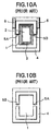
- a mirror 2 and a drive coil 3 are formed on the same face (surface side) of the movable portion 1 shown in FIG. 10 (A) so that the drive coil electrode terminals are positioned on the surface side of the semiconductor substrate.
- the drive coil 3 is arranged around the mirror 2 shown in the figure so that the mirror 2 and the drive coil 3 do not overlap.
- FIG. 10(B) shows the rear surface side of the optical scanning apparatus.
- 4 denotes the semiconductor substrate
- 5A and 5B denote axial support portions of a torsion bar structure for axially supporting the movable portion 1 so as to swing relative to the semiconductor substrate 4
- 6 denotes the electrode terminal of the drive coil 3.
- the present invention takes into consideration the above situation with the object of providing a planar type optical scanning apparatus that, by arranging the mirror on one face of the movable portion and the drive coil on the other face, enables further miniaturization, and in turn can achieve cost reduction.
- a movable portion and an axial support portion for axially supporting the movable portion so as to be able to swing are integrally formed on a semiconductor substrate, a mirror is provided on the surface side of the movable portion, a drive coil is provided on the rear face side of the movable portion, and there is provided a magnetic field generation device for applying a static magnetic field to the drive coil, the construction being such that the movable portion is driven by a magnetic force generated by passing a current through the drive coil.
- a cavity for allowing swinging movement of the movable portion of the optical scanning apparatus, and a conductive pattern are provided in an optical scanning apparatus fixing region of the mounting substrate, the construction being such that when the optical scanning apparatus is fitted in the fixing region, a drive coil electrode terminal provided on the rear face of the semiconductor substrate of the optical scanning apparatus, and the conductive pattern make contact
- the optical scanning apparatus when the optical scanning apparatus is fitted on the mounting substrate, since the drive coil electrode terminals of the optical scanning apparatus side can be electrically connected to terminal pins of the mounting substrate via the conductive patterns, even if the drive coil is formed on the rear face side, the optical scanning apparatus can be easily mounted on the mounting substrate.
- the construction of the mounting substrate is such that terminal pins for feeding out electrodes that are electrically connected to the conductive pattern are fixed at the periphery of the fixing region. Hence it is possible to connect to the outside by the terminal pins using a one-touch operation.
- the construction is such that solder surfaces are formed on the conductive pattern and the drive coil electrode terminal, respectively, and the two solder surfaces are thermo compression bonded to fix the optical scanning apparatus to the fixing region of the mounting substrate. Hence it is possible to secure the optical scanning apparatus and connect the electrode terminals at the same time.
- the structure has an auxiliary substrate provided with a cavity for allowing swinging movement of a movable portion of the optical scanning apparatus, and a conductive pattern at least at the periphery of the cavity of the rear face side, the construction being such that the optical scanning apparatus is fixed on the rear face of the auxiliary substrate from the surface side, and drive coil electrode terminals provided on the rear face of the optical scanning apparatus and the conductive pattern of the auxiliary substrate are electrically connected, while, above the mounting substrate on which a plurality of terminal pins are fitted through to the surface side thereof, the auxiliary substrate is fixed at a distance, with an intervening spacer, so that the protruding ends of the terminal pins on the surface side of the mounting substrate and the conductive pattern are electrically connected.
- the construction may be such that the auxiliary substrate has a plurality of through holes in the periphery of the cavity, and has the conductive pattern for electrically connecting the surface side and the rear face side via the through holes, and the protruding ends of the terminal pins on the surface side of the mounting substrate are passed through the through holes of the auxiliary substrate to solder the terminal pins protruding from the surface side of the auxiliary substrate.
- FIG. 1 and FIG. 2 show the construction of an embodiment of the optical scanning apparatus according to the present invention.
- an optical scanning apparatus 10 has a planar movable plate 12 being a movable portion and torsion bars 13A, 13B serving as axial support portions for axially supporting the movable plate 12 to a silicon substrate 11 serving as a semiconductor substrate, integrally formed by anisotropic etching on, for example, the silicon substrate 11.
- the thickness of the movable plate 12 is made thin compared with the thickness of the silicon substrate 11, so that the movable plate 12 can swing about the axial support portion.
- a mirror 14 formed, for example, by aluminum vapor deposition.
- a drive coil 15 of copper thin film formed, for example, using an electro-typing method or the like.
- a pair of electrode terminals 16A, 16B are formed similarly to the drive coil 15, by an electro-typing method or the like.
- One end of the drive coil 15 is electrically connected to one of the electrode terminals 16A by way of one of the torsion bars 13A, and the other end of the drive coil 15 is electrically connected to the other electrode terminal 16B by way of the other torsion bar 13B.
- a plurality of solder surfaces 22 for fixing the optical scanning apparatus 10 onto a package substrate in a mounting structure is provided on the rear face side of the silicon substrate 11.
- Insulation plates 17, 18 are fixed onto the surface and rear face of the silicon substrate 11. On the surface side insulation plate 17, an open portion 17a is provided so that the movable plate 12 can swing about the axial support portion.
- the insulation plates 17, 18 are provided with permanent magnets 19A, 19B and 20A, 20B serving as pairs of magnetic field generation devices for applying static magnetic fields to the drive coil 15 part, on opposite sides of the movable plate 12 parallel to the axis of the torsion bars 13A, 13B.
- one pair of the permanent magnets 19A, 19B is arranged such that the bottom side thereof is the north pole, and the upper side the south pole, and the other pair of permanent magnets 20A, 20B is arranged such that the bottom side thereof is the south pole, and the upper side the north pole.
- the optical scanning apparatus 10 of this construction since the mirror 14 is formed on the surface side of the movable plate 12, and the drive coil 15 is formed on the rear face side of the movable plate 12, in comparison with the case where the mirror and the drive coil are formed on only the surface side of the movable plate as in the conventional apparatus shown in FIG. 10, if the area of the mirror 14 is the same, the area of the movable plate 12 can be reduced by the formation area of the conventional drive coil, thus enabling miniaturization of the optical scanning apparatus 10.
- the number of chips produced on one wafer is increased.
- the cost for one wafer is the same wherever the same process is used. Therefore, by increasing the number of chips that can be produced on one wafer, the cost can be reduced accordingly, thus enabling reduction of manufacturing costs as well as miniaturization of the optical scanning apparatus 10.
- the area of the movable plate 12 is the same as in the conventional apparatus, the area of the mirror 1 can be enlarged so that there is an advantage in that a larger mirror can be produced at the same cost as a conventional one.
- a current is passed through the drive coil 15 with one electrode terminal 16A as a positive pole and the other electrode terminal 16B as a negative pole.
- a magnetic field is formed by means of the permanent magnets 19A, 19B and 20A, 20B on opposite sides of the movable plate 12, in a direction so as to intersect the drive coil 15 lying along the planar face of the movable plate 12, as shown by arrows in FIG. 1.
- a current flows in the drive coil 15 positioned in this magnetic field, a magnetic force acts on the opposite sides of the movable plate 12 based on the aforementioned equation (1), in a direction according to Fleming's left hand rule, and the movable plate 12 rotates.
- the torsion bars 13A, 13B are twisted with the rotation of the movable portion, producing a spring reaction force in the torsion bars 13A, 13B.
- the movable plate 12 rotates to a position where this spring reaction force and the magnetic force are in equilibrium.
- the angle of rotation of the movable plate 12 is proportional to the current flowing in the drive coil 15. Therefore, by controlling the current amount in the drive coil 15, the rotation angle of the movable plate 12 can be controlled.
- the direction of reflection of a laser beam incident on the mirror 14 in a plane perpendicular to the axis of the torsion bars 13A, 13B can be freely controlled. Hence laser scanning is possible by continuous cyclical operation of the rotation angle of the mirror 14.
- a package substrate 31 serving as a mounting substrate, on which the optical scanning apparatus 10 is mounted is provided with a cavity 32 for allowing swinging movement of the movable plate 12 of the optical scanning apparatus 10, as shown in FIG. 5, in the fixed area of the optical scanning apparatus, positioned almost centrally on the substrate.
- a pair of conductive patterns 33 which are electrically connected to the electrode terminals 16A, 16B on the rear face of the optical scanning apparatus 10, and other conductive patterns 33, and solder faces 34 serving as fixing parts for fitting the optical scanning apparatus 10 are provided.
- Solder faces are also formed on extensions 33A, 33B of the conductive patterns 33, to serve as complementary fixing parts to the solder faces 34.
- two terminal pins 35 which electrically connect to the conductive patterns 33, and other two terminal pins 35 are provided, such that the pins pass through and protrude from the surface side of the substrate 31 via through holes.
- the permanent magnets 37 and 38 are arranged with the optical scanning apparatus 10 between them.
- the arrangement of the permanent magnets is not limited to the construction of this embodiment, and the arrangement may be above and below as shown in FIG. 1.
- the process of mounting the optical scanning apparatus 10 on the package substrate 31 is such that, as shown by the arrows in FIG. 5, the optical scanning apparatus 10 is mounted on the fixed area located almost in the center of the surface of the package substrate 31 from above.
- the mounting is such that solder faces formed on the electrode terminals 16A, 16B of the drive coil on the rear face of the optical scanning apparatus 10 make contact with the solder faces of the extensions 33A, 33B of the conductive patterns 33, and the solder faces 22 on the rear face of the optical scanning apparatus 10 contact the solder faces 34, 34 on the package substrate 31 side.
- a thermo compression bonding process is applied, so that the solder faces contacting each other are bonded, to fix the optical scanning apparatus 10 onto the package substrate 31.
- the optical scanning apparatus 10 is mounted on the package substrate 31.
- the electrode terminals 16A, 16B on the optical scanning apparatus 10 side can be electrically connected to the extensions 33A, 33B of the conductive patterns 33 on the package substrate 31 side. Therefore, even in the case where the drive coil 15 is provided on the rear face side of the movable plate 12, the electrode terminals 16A, 16B of the drive coil 15 can be electrically connected to the terminal pins 35 of the package substrate 31 so that the electrodes can be easily fed to the outside. Since swinging movement of the movable plate 12 can be allowed by the cavity 32 of the package substrate 31, there is no impediment to the operation of the optical scanning apparatus 10.
- the fixing method of the optical scanning apparatus 10 is not limited to the embodiment.
- a construction without terminal pins may be used.
- the optical scanning apparatus 10 can also be easily mounted even though the drive coil 15 is provided on the rear face of the movable plate 12. However, it is necessary to provide the cavity 32 for enabling swinging movement of the movable plate 12, in the package substrate 31. Therefore, there is a concern that the strength of the package substrate 31 may be reduced.
- FIG. 6 shows the mounting structure of a fifth aspect of the present invention, in which an optical scanning apparatus provided with only a drive coil on the rear face of a movable plate can be easily mounted on a package substrate, without reducing the strength of the package substrate.
- an optical scanning apparatus provided with only a drive coil on the rear face of a movable plate can be easily mounted on a package substrate, without reducing the strength of the package substrate.
- the construction is such that an auxiliary substrate 42 is fixed to a package substrate 31' at a distance from a package substrate 31', by interposing spacers 41, and the optical scanning apparatus 10 is fixed onto the rear face of the auxiliary substrate 42, that is, between the package substrate 31' and the auxiliary substrate 42.
- the permanent magnets 37, 38 and the frame-like yoke 36 are provided on the surface of the package substrate 31'.
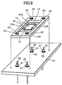
- the auxiliary substrate 42 as shown in FIG. 7 through FIG. 9, has a cavity 42a for allowing swinging movement of the movable plate 12 of the optical scanning apparatus 10, and the through holes 43 in four points at the periphery of the cavity 42a. Furthermore, conductive patterns 44, 45, electrically conducting via the through holes 43, are provided on the surface and rear face of the auxiliary substrate 42. The conductive patterns 45 on the rear face side have extensions 45a, for connecting to the drive coil electrode terminals 16A, 16B on the optical scanning apparatus 10.
- the package substrate 31' is formed similarly to the package substrate 31 of the embodiment of FIG. 4 except that it has no cavity.
- a mounting process of the optical scanning apparatus 10 of the embodiment is described based on FIG. 7 through FIG. 9.
- the optical scanning apparatus 10 With the rear face side of the auxiliary substrate 42 facing upward, the optical scanning apparatus 10 is fitted onto the fixed area positioned approximately centrally on the auxiliary substrate 42 from above as shown by the arrows in FIG. 7, in a condition with the rear face side of the optical scanning apparatus 10 facing upward.
- the electrode terminals 16A, 16B on the optical scanning apparatus 10 side, and the extensions 45a, 45a of the conductive patterns 45 on the rear face side of the auxiliary substrate 42 are electrically connected by bonding wires 46. The situation is shown in FIG. 8.
- the auxiliary substrate 42 is reversed so that the surface side of the auxiliary substrate 42 faces upward.
- the face of the mirror 14 of the optical scanning apparatus 10 faces upward.
- the spacers 41 and the auxiliary substrate 42 are installed sequentially to each protruding end of terminal pins 35 of the package substrate 31' to fix the auxiliary substrate 42 on the package substrate 31'.
- the terminal pins 35 protruding from the surface side of the auxiliary substrate 42 are soldered to fix the auxiliary substrate 42 to the package substrate 31'.
- the electrode terminals 16A, 16B of the drive coil 15 of the optical scanning apparatus 10 are electrically connected to the terminal pins 35 via the conductive patterns 43, 44 and the solder fixing.
- the electrode terminals 16A, 16B of the drive coil 15 can be electrically connected to the terminal pins 35 of the package substrate 31', and the electrodes can be easily fed to the outside. Moreover, since the package substrate 31' has no cavity the strength of the package substrate 31' is improved in comparison with the mounting structure in FIG. 4.
- the area of the movable portion can be reduced so that the optical scanning apparatus can be miniaturized. Consequently, since the number of chips produced on one wafer is increased, the cost can be reduced accordingly, thus enabling reduction of manufacturing costs. Furthermore, if the area of the movable portion is the same as a conventional apparatus, the area of the mirror can be enlarged so that there is an advantage in that a larger mirror can be produced at the same cost as a conventional one.
- the electrode terminals on the optical scanning apparatus side can be electrically connected to the terminal pins on the mounting substrate side. Therefore, even in the case where the drive coil is provided on the rear face side of the movable portion, the electrodes of the optical scanning apparatus can easily be fed outside.
- the conductive patterns can also serve as part of the fixed area, and fitting of the optical scanning apparatus and connection of the electrode terminals are possible at the same time.
- a mounting structure in which an auxiliary substrate is fitted above the mounting substrate via spacers, and a cavity is formed in the auxiliary substrate to fix the optical scanning apparatus even in the case where the drive coil is provided on the rear face side of the movable portion, it is possible to feed out the electrodes of the optical scanning apparatus easily. Furthermore, a cavity for allowing swinging movement of the movable portion of the optical scanning apparatus does not need to be formed in the mounting substrate, and hence the strength of the mounting substrate can be improved.
- the present invention enables miniaturization and cost reduction of a planar type optical scanning apparatus that is manufactured using semiconductor manufacturing technology, and hence miniaturization and cost reduction of various apparatuses which incorporate this planar type optical scanning apparatus can be realized. Therefore the industrial applicability is considerable.
Landscapes
- Physics & Mathematics (AREA)
- General Physics & Mathematics (AREA)
- Optics & Photonics (AREA)
- Electromagnetism (AREA)
- Engineering & Computer Science (AREA)
- Computer Hardware Design (AREA)
- Theoretical Computer Science (AREA)
- Mechanical Optical Scanning Systems (AREA)
- Facsimile Scanning Arrangements (AREA)
- Investigating Or Analysing Materials By The Use Of Chemical Reactions (AREA)
Abstract
Description
Claims (6)
- A planar type optical scanning apparatus,wherein a movable portion and an axial support portion for axially supporting said movable portion so as to be able to swing, are integrally formed on a semiconductor substrate, a mirror is provided on the surface side of said movable portion, a drive coil is provided on the rear face side of said movable portion, and there is provided a magnetic field generation device for applying a static magnetic field to said drive coil, andwherein said movable portion is driven by a magnetic force generated by passing a current through said drive coil.
- A mounting structure for mounting the planar type optical scanning apparatus recited in claim 1 on a mounting substrate, wherein a cavity for allowing swinging movement of the movable portion of the optical scanning apparatus, and a conductive pattern are provided in an optical scanning apparatus fixing region of said mounting substrate, and, when said optical scanning apparatus is fitted in said fixing region, a drive coil electrode terminal provided on the rear face of the semiconductor substrate of the optical scanning apparatus, and said conductive pattern make contact.
- A mounting structure for a planar type optical scanning apparatus according to claim 2, wherein said mounting substrate fixes terminal pins for feeding out electrodes that are electrically connected to said conductive pattern at the periphery of said fixing region.
- A mounting structure for a planar type optical scanning apparatus according to either one of claim 2 and claim 3, wherein solder surfaces are formed on said conductive pattern and said drive coil electrode terminal, respectively, and the two solder surfaces are thermo compression bonded to fix the optical scanning apparatus to the fixing region of said mounting substrate.
- A mounting structure for mounting the planar type optical scanning apparatus recited in claim 1 on a mounting substrate,wherein said structure has an auxiliary substrate provided with a cavity allowing swinging movement of a movable portion of the optical scanning apparatus, and a conductive pattern at least at the periphery of said cavity of the rear face side, andwherein said optical scanning apparatus is fixed on the rear face of said auxiliary substrate from the surface side, and drive coil electrode terminals provided on the rear face of the optical scanning apparatus and the conductive pattern of said auxiliary substrate are electrically connected, while, above said mounting substrate on which a plurality of terminal pins are fitted through to the surface side thereof, said auxiliary substrate is fixed at a distance, with an intervening spacer, so that the protruding ends of the terminal pins on the surface side of said mounting substrate and the conductive pattern of said auxiliary substrate are electrically connected.
- A mounting structure for a planar type optical scanning apparatus according to claim 5, wherein said auxiliary substrate has a plurality of through holes in the periphery of said cavity and said conductive pattern for electrically connecting the surface side and the rear face side via said through holes, and the protruding ends of the terminal pins on the surface side of said mounting substrate are passed through the through holes of said auxiliary substrate to solder the terminal pins protruding from the surface side of said auxiliary substrate.
Applications Claiming Priority (3)
| Application Number | Priority Date | Filing Date | Title |
|---|---|---|---|
| JP5180599 | 1999-02-26 | ||
| JP05180599A JP4111619B2 (en) | 1999-02-26 | 1999-02-26 | Mounting structure of planar optical scanning device |
| PCT/JP2000/001132 WO2000050950A1 (en) | 1999-02-26 | 2000-02-25 | Planar optical scanner and its mounting structure |
Publications (4)
| Publication Number | Publication Date |
|---|---|
| EP1087248A1 true EP1087248A1 (en) | 2001-03-28 |
| EP1087248A4 EP1087248A4 (en) | 2006-06-21 |
| EP1087248B1 EP1087248B1 (en) | 2011-03-16 |
| EP1087248B8 EP1087248B8 (en) | 2011-10-05 |
Family
ID=12897147
Family Applications (1)
| Application Number | Title | Priority Date | Filing Date |
|---|---|---|---|
| EP00905374A Expired - Lifetime EP1087248B8 (en) | 1999-02-26 | 2000-02-25 | Planar optical scanner and its mounting structure |
Country Status (7)
| Country | Link |
|---|---|
| US (1) | US6456413B1 (en) |
| EP (1) | EP1087248B8 (en) |
| JP (1) | JP4111619B2 (en) |
| KR (1) | KR100712297B1 (en) |
| AT (1) | ATE502319T1 (en) |
| DE (1) | DE60045730D1 (en) |
| WO (1) | WO2000050950A1 (en) |
Cited By (4)
| Publication number | Priority date | Publication date | Assignee | Title |
|---|---|---|---|---|
| EP1207416A1 (en) * | 2000-11-20 | 2002-05-22 | Olympus Optical Co., Ltd. | Optical deflector |
| WO2008019753A1 (en) * | 2006-08-18 | 2008-02-21 | Oc Oerlikon Balzers Ag | Mirror drive for projection systems and associated method |
| US7420449B2 (en) | 2006-08-18 | 2008-09-02 | Oc Oerlikon Balzers Ag | Mirror actuating device for projection systems |
| EP3064975A1 (en) * | 2015-03-06 | 2016-09-07 | Ricoh Company, Ltd. | Optical scanning apparatus, substrate fixing method in optical scanning apparatus, image display apparatus, and vehicle |
Families Citing this family (11)
| Publication number | Priority date | Publication date | Assignee | Title |
|---|---|---|---|---|
| JP4544734B2 (en) * | 2000-12-21 | 2010-09-15 | シチズンファインテックミヨタ株式会社 | Planar type galvanometer mirror |
| JP4641378B2 (en) * | 2004-02-16 | 2011-03-02 | キヤノン株式会社 | Optical scanning device and image display device having the same |
| JP2005292381A (en) | 2004-03-31 | 2005-10-20 | Canon Inc | Optical deflector |
| JP4969136B2 (en) * | 2006-04-13 | 2012-07-04 | 日本信号株式会社 | Actuator manufacturing method |
| JP2009014762A (en) * | 2007-06-29 | 2009-01-22 | Olympus Corp | Micromirror device |
| JP5252872B2 (en) * | 2007-09-28 | 2013-07-31 | 日本信号株式会社 | Planar type electromagnetic actuator |
| JP2009154264A (en) * | 2007-12-27 | 2009-07-16 | Stanley Electric Co Ltd | MEMS module |
| WO2015092907A1 (en) * | 2013-12-19 | 2015-06-25 | パイオニア株式会社 | Drive device |
| JP2016006445A (en) * | 2014-06-20 | 2016-01-14 | 船井電機株式会社 | Vibration mirror package and projector |
| JP7015653B2 (en) * | 2017-08-10 | 2022-02-03 | 浜松ホトニクス株式会社 | Optical module and manufacturing method of optical module |
| JP6546370B1 (en) * | 2017-12-01 | 2019-07-17 | 浜松ホトニクス株式会社 | Actuator device |
Family Cites Families (12)
| Publication number | Priority date | Publication date | Assignee | Title |
|---|---|---|---|---|
| US4421381A (en) | 1980-04-04 | 1983-12-20 | Yokogawa Hokushin Electric Corp. | Mechanical vibrating element |
| JPS60107017A (en) | 1983-11-16 | 1985-06-12 | Hitachi Ltd | light deflection element |
| JP2924200B2 (en) | 1990-01-18 | 1999-07-26 | 富士電機株式会社 | Torsional vibrator and its application element |
| JPH04100358A (en) * | 1990-08-17 | 1992-04-02 | Matsushita Electric Ind Co Ltd | cell transfer circuit |
| DE4100358A1 (en) | 1991-01-05 | 1992-07-09 | Robotron Bueromasch Ag | Vibrating mirror arrangement for deflection of optical beam - is set into oscillation by alternating current excitation of coil arrangement on back of semiconductor reflector |
| US5629790A (en) * | 1993-10-18 | 1997-05-13 | Neukermans; Armand P. | Micromachined torsional scanner |
| JP2722314B2 (en) | 1993-12-20 | 1998-03-04 | 日本信号株式会社 | Planar type galvanometer mirror and method of manufacturing the same |
| JP2657769B2 (en) | 1994-01-31 | 1997-09-24 | 正喜 江刺 | Planar type galvanometer mirror having displacement detection function and method of manufacturing the same |
| KR100343219B1 (en) | 1995-02-25 | 2002-11-23 | 삼성전기주식회사 | Apparatus for driving mirror |
| JP2987750B2 (en) * | 1995-05-26 | 1999-12-06 | 日本信号株式会社 | Planar type electromagnetic actuator |
| JP4414498B2 (en) * | 1997-12-09 | 2010-02-10 | オリンパス株式会社 | Optical deflector |
| DE29801643U1 (en) * | 1998-01-31 | 1998-06-04 | CMS Mikrosysteme GmbH Chemnitz, 09125 Chemnitz | Micromechanical and electromagnetically operated mirror arrangements |
-
1999
- 1999-02-26 JP JP05180599A patent/JP4111619B2/en not_active Expired - Fee Related
-
2000
- 2000-02-25 AT AT00905374T patent/ATE502319T1/en not_active IP Right Cessation
- 2000-02-25 WO PCT/JP2000/001132 patent/WO2000050950A1/en not_active Ceased
- 2000-02-25 US US09/673,269 patent/US6456413B1/en not_active Expired - Fee Related
- 2000-02-25 EP EP00905374A patent/EP1087248B8/en not_active Expired - Lifetime
- 2000-02-25 KR KR1020007011838A patent/KR100712297B1/en not_active Expired - Fee Related
- 2000-02-25 DE DE60045730T patent/DE60045730D1/en not_active Expired - Lifetime
Cited By (5)
| Publication number | Priority date | Publication date | Assignee | Title |
|---|---|---|---|---|
| EP1207416A1 (en) * | 2000-11-20 | 2002-05-22 | Olympus Optical Co., Ltd. | Optical deflector |
| US6888656B2 (en) | 2000-11-20 | 2005-05-03 | Olympus Corporation | Optical deflector |
| WO2008019753A1 (en) * | 2006-08-18 | 2008-02-21 | Oc Oerlikon Balzers Ag | Mirror drive for projection systems and associated method |
| US7420449B2 (en) | 2006-08-18 | 2008-09-02 | Oc Oerlikon Balzers Ag | Mirror actuating device for projection systems |
| EP3064975A1 (en) * | 2015-03-06 | 2016-09-07 | Ricoh Company, Ltd. | Optical scanning apparatus, substrate fixing method in optical scanning apparatus, image display apparatus, and vehicle |
Also Published As
| Publication number | Publication date |
|---|---|
| JP2000249964A (en) | 2000-09-14 |
| EP1087248B8 (en) | 2011-10-05 |
| JP4111619B2 (en) | 2008-07-02 |
| WO2000050950A1 (en) | 2000-08-31 |
| US6456413B1 (en) | 2002-09-24 |
| DE60045730D1 (en) | 2011-04-28 |
| EP1087248A4 (en) | 2006-06-21 |
| KR20010034830A (en) | 2001-04-25 |
| ATE502319T1 (en) | 2011-04-15 |
| EP1087248B1 (en) | 2011-03-16 |
| KR100712297B1 (en) | 2007-05-02 |
Similar Documents
| Publication | Publication Date | Title |
|---|---|---|
| US5912608A (en) | Planar type electromagnetic actuator | |
| US6456413B1 (en) | Planar type optical scanning apparatus and mounting structure thereof | |
| KR102522700B1 (en) | Camera module and camera device including the same | |
| US12273998B2 (en) | Substrate for image sensor | |
| JP2560629B2 (en) | Silicon micro relay | |
| JP3425814B2 (en) | Electromagnetic actuator and method of manufacturing the same | |
| US20080100898A1 (en) | Electromagnetic micro-actuator | |
| CN1498412A (en) | Micromagnetic Latch Switch with Permanent Magnet Slack Alignment Requirement | |
| US6888656B2 (en) | Optical deflector | |
| JPH08334723A (en) | Optical deflection element | |
| JP4036643B2 (en) | Optical deflector and optical deflector array | |
| JP2005099063A (en) | Deflection actuator, optical scanning element, and light receiving scanning element | |
| JP2007014130A (en) | Planar-type electromagnetic actuator | |
| KR100573709B1 (en) | Electronic actuator and its manufacturing method | |
| WO2014162521A1 (en) | Actuator | |
| JP2008026649A (en) | Planar type actuator and optical attenuator using the same | |
| US20240027747A1 (en) | Optical module | |
| JP4404560B2 (en) | Planar type electromagnetic actuator | |
| TW202534985A (en) | Spring piece structure and voice coil motor | |
| JP2007252124A (en) | Electromagnetic actuator | |
| JP2004258157A (en) | Planar type electromagnetic actuator |
Legal Events
| Date | Code | Title | Description |
|---|---|---|---|
| PUAI | Public reference made under article 153(3) epc to a published international application that has entered the european phase |
Free format text: ORIGINAL CODE: 0009012 |
|
| 17P | Request for examination filed |
Effective date: 20001117 |
|
| AK | Designated contracting states |
Kind code of ref document: A1 Designated state(s): AT BE CH CY DE DK ES FI FR GB GR IE IT LI LU MC NL PT SE |
|
| RBV | Designated contracting states (corrected) |
Designated state(s): AT DE FR GB |
|
| A4 | Supplementary search report drawn up and despatched |
Effective date: 20060523 |
|
| 17Q | First examination report despatched |
Effective date: 20080128 |
|
| GRAP | Despatch of communication of intention to grant a patent |
Free format text: ORIGINAL CODE: EPIDOSNIGR1 |
|
| GRAS | Grant fee paid |
Free format text: ORIGINAL CODE: EPIDOSNIGR3 |
|
| GRAA | (expected) grant |
Free format text: ORIGINAL CODE: 0009210 |
|
| AK | Designated contracting states |
Kind code of ref document: B1 Designated state(s): AT DE FR GB |
|
| REG | Reference to a national code |
Ref country code: GB Ref legal event code: FG4D |
|
| REF | Corresponds to: |
Ref document number: 60045730 Country of ref document: DE Date of ref document: 20110428 Kind code of ref document: P |
|
| REG | Reference to a national code |
Ref country code: DE Ref legal event code: R096 Ref document number: 60045730 Country of ref document: DE Effective date: 20110428 |
|
| RIN2 | Information on inventor provided after grant (corrected) |
Inventor name: ASADA, NORIHIRO,T |
|
| PG25 | Lapsed in a contracting state [announced via postgrant information from national office to epo] |
Ref country code: AT Free format text: LAPSE BECAUSE OF FAILURE TO SUBMIT A TRANSLATION OF THE DESCRIPTION OR TO PAY THE FEE WITHIN THE PRESCRIBED TIME-LIMIT Effective date: 20110316 |
|
| PLBE | No opposition filed within time limit |
Free format text: ORIGINAL CODE: 0009261 |
|
| STAA | Information on the status of an ep patent application or granted ep patent |
Free format text: STATUS: NO OPPOSITION FILED WITHIN TIME LIMIT |
|
| 26N | No opposition filed |
Effective date: 20111219 |
|
| REG | Reference to a national code |
Ref country code: DE Ref legal event code: R097 Ref document number: 60045730 Country of ref document: DE Effective date: 20111219 |
|
| GBPC | Gb: european patent ceased through non-payment of renewal fee |
Effective date: 20120225 |
|
| REG | Reference to a national code |
Ref country code: FR Ref legal event code: ST Effective date: 20121031 |
|
| PG25 | Lapsed in a contracting state [announced via postgrant information from national office to epo] |
Ref country code: GB Free format text: LAPSE BECAUSE OF NON-PAYMENT OF DUE FEES Effective date: 20120225 Ref country code: FR Free format text: LAPSE BECAUSE OF NON-PAYMENT OF DUE FEES Effective date: 20120229 |
|
| PGFP | Annual fee paid to national office [announced via postgrant information from national office to epo] |
Ref country code: DE Payment date: 20130228 Year of fee payment: 14 |
|
| REG | Reference to a national code |
Ref country code: DE Ref legal event code: R119 Ref document number: 60045730 Country of ref document: DE |
|
| REG | Reference to a national code |
Ref country code: DE Ref legal event code: R119 Ref document number: 60045730 Country of ref document: DE Effective date: 20140902 |
|
| PG25 | Lapsed in a contracting state [announced via postgrant information from national office to epo] |
Ref country code: DE Free format text: LAPSE BECAUSE OF NON-PAYMENT OF DUE FEES Effective date: 20140902 |