EP1085793A2 - Kompakte elektrische Vorrichtung, insbesondere Schaltnetzteil - Google Patents
Kompakte elektrische Vorrichtung, insbesondere Schaltnetzteil Download PDFInfo
- Publication number
- EP1085793A2 EP1085793A2 EP00118458A EP00118458A EP1085793A2 EP 1085793 A2 EP1085793 A2 EP 1085793A2 EP 00118458 A EP00118458 A EP 00118458A EP 00118458 A EP00118458 A EP 00118458A EP 1085793 A2 EP1085793 A2 EP 1085793A2
- Authority
- EP
- European Patent Office
- Prior art keywords
- electrical
- carrier body
- transformer
- compact
- primary
- Prior art date
- Legal status (The legal status is an assumption and is not a legal conclusion. Google has not performed a legal analysis and makes no representation as to the accuracy of the status listed.)
- Granted
Links
Images


Classifications
-
- H—ELECTRICITY
- H05—ELECTRIC TECHNIQUES NOT OTHERWISE PROVIDED FOR
- H05K—PRINTED CIRCUITS; CASINGS OR CONSTRUCTIONAL DETAILS OF ELECTRIC APPARATUS; MANUFACTURE OF ASSEMBLAGES OF ELECTRICAL COMPONENTS
- H05K1/00—Printed circuits
- H05K1/02—Details
- H05K1/14—Structural association of two or more printed circuits
- H05K1/144—Stacked arrangements of planar printed circuit boards
-
- H—ELECTRICITY
- H02—GENERATION; CONVERSION OR DISTRIBUTION OF ELECTRIC POWER
- H02M—APPARATUS FOR CONVERSION BETWEEN AC AND AC, BETWEEN AC AND DC, OR BETWEEN DC AND DC, AND FOR USE WITH MAINS OR SIMILAR POWER SUPPLY SYSTEMS; CONVERSION OF DC OR AC INPUT POWER INTO SURGE OUTPUT POWER; CONTROL OR REGULATION THEREOF
- H02M7/00—Conversion of AC power input into DC power output; Conversion of DC power input into AC power output
- H02M7/003—Constructional details, e.g. physical layout, assembly, wiring or busbar connections
Definitions
- the invention relates to a compact electrical device, in particular Switching power supply, with at least one inductor and one with one Reference voltage connectable contacting device, the inductance with the contacting device via a first electrically conductive Connection is connected.
- the invention is therefore based on the object of an electrical device specify which is a reduction in assembly effort enables and still works reliably.
- the object is achieved in that the inductance and / or the first electrically conductive connection and / or the contacting device in a carrier body made of insulating material are at least partially arranged and by the material of the carrier body are isolated from each other, with an electrical circuit over a second electrically conductive connection with the first electrically conductive connection of the support body is connected.
- the advantage of the invention is that different electrical Components combined into a mechanically connected unit be, thereby mechanical stability of the device is achieved.
- the manufacturing costs and the manufacturing costs of electrical device are thereby greatly reduced.
- Such a The electronics block contains all the necessary electrical conductor tracks, either by temporary spacers or real insulation layers or Layers insulated from each other and then with plastic be encapsulated. In addition to reducing the number of work steps, this also includes: an improvement in the electrical properties in terms of insulation reached.
- this compact electronics is shockproof and has vibration-reduced properties, which is particularly useful for the Use in motor vehicles is advantageous.
- Two inductors arranged on the carrier body are advantageous as a transformer for matching different electrical Voltages between the electrical circuit and the contacting device formed, the first electrical connections Primary winding of the transformer with the contacting device and the Secondary winding of the transformer with the electrical circuit connect, the primary and secondary winding at least one Enclose part of a transformer core.
- the object of the invention is achieved in that the Transformer core and / or the first electrically conductive connections and / or the contacting device in an insulating material existing carrier body are arranged, the first electrical Connections to each other through the material of the carrier body are isolated and the primary and secondary winding of the transformer a flat carrier element carrying the electrical circuit are arranged that the transformer core is enclosed by the windings and a second electrically conductive connection with the first electrical connection of the carrier body is connected.
- the individual components are plugs, power supply / distribution as well as the transformer windings or the transformer core arranged together in a compact unit and have the advantages already explained.
- the second is electrically conductive Connection of at least one contact pin on the carrier element Connection of the electrical circuit to at least one conductor track arranged of the carrier body, which in one with the at least one Conductor protrudes electrically connected opening.
- This arrangement of the rigid pin makes the electrical connection between the electrical circuit and the electrically conductive parts of the carrier body simply by plugging the carrier body onto the Contact pin realized, which at the same time creates a mechanical lock is achieved.
- This electrical connection can be made particularly easily if the contact pin for making the electrical connection in the opening of the carrier body is pressed. This means that not only an electrical, but also create a permanent mechanical connection, which is insensitive to vibrations.
- the ends are those designed as a conductor track first electrical connection from the opening of the carrier body this led out outstandingly, and together with that by the Soldered through the opening of the contact pin.
- electrical components such as ELKO's or choke coils arranged so they can be soldered in one soldering operation of the contact pin are attached to the carrier body. This is also valid for additional circuit boards with wired components that can also be assembled in the same soldering process.
- the conductor tracks can be produced particularly easily if they are used as Sheet metal parts are formed. With the help of such layered Stamped metal sheets, which the electrical conductor tracks in the carrier body form, the carrier body can be easily manufactured as an injection molded part.
- the body of the contactor is formed by the carrier body.
- the carrier body is for subsequent Inclusion of further electrical and / or electronic Components trained.
- it has one with locking devices provided recording for another component.
- So can be advantageously housed on the outside of the support body or unhoused electronic components can be arranged.
- the compact electrical block can be molded in the same plastic design such that the carrier body is part of a housing, which covers the electrical circuit of the supporting carrier element.
- the carrier body has a circumferential, angled collar on which rests on the carrier element, one on the collar circumferential seal is also molded.
- the carrier body is a middle part of the housing with a gasket molded on one side to rest on the support element formed, the housing middle part with a flat cover is closed, which also has a molded seal, which rests on the middle part of the housing.
- the carrier element is made of metal, preferably made of aluminum and also used for heat dissipation for the power components.
- the carrier element is a substrate which is made of copper applied to heat-conducting ceramic (Direct Copper Bonding) exists. Due to the very good heat conduction of this material are high performance of the power transistors enables.
- the Transformer core is constructed in two parts, with a first E-like Core element rests on the carrier element, the three of which are perpendicular to the Carrier element pioneering webs through corresponding transformer openings grab the support body and a second flat or E-like trained core element covers the webs and magnetically connects with each other, with the primary and secondary winding rotating are arranged between the webs.
- the transformer By resting the first core element on the as a heat sink trained carrier element is the transformer with high performance operable and can have a high efficiency.
- the transformer works reliably with those in modern motor vehicles occurring high currents and can be easily cooled.
- the primary and secondary windings protrude the transformer laterally interrupted from the carrier body out, the one-piece having an eight-like cross section Transformer core over the interrupted primary and secondary windings is pushed, after sliding on the transformer core the primary and secondary windings are electrically welded or soldered getting closed.
- Carrier body end part which adapted to the windings Contains conductor tracks, the primary and secondary winding electrical closed.
- the primary and secondary windings of the transformer are parallel arranged to the flat support element.
- a switching power supply is shown as it is used to adapt different voltage levels in numerous electrical devices Used.
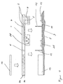
- a carrier body 1 made of plastic includes several superimposed conductor tracks 2, which as Stamped bending sheets are formed.
- the conductor tracks 2 are like this arranged within the plastic carrier body 1 that the plastic between the conductor tracks 2 has an insulating effect.
- the Carrier body 1 windings 3a, 3b which are a primary and a secondary winding form a planar transformer.
- the primary 3a and the secondary winding 3b is formed by at least one turn.
- Some conductor tracks 2 are bent out of the plastic carrier body 1, the ends of which form connector pins 4 and the plastic carrier body 1 forms the connector body 5 at the same time by means of an injection molding process.
- the plastic body 1 has metallized contact openings 6 and 7, which are connected to the conductor tracks 2 and into which contact pins 12, which are arranged on an aluminum carrier element 8, engage.
- a ceramic circuit board 9, which has copper tracks 10, is fastened on the carrier element 8.
- the ceramic circuit board 9 is glued to the aluminum body 8, for example.
- the copper tracks 10 represent an electrical connection between the power components 11, which are likewise arranged on the printed circuit board 9, and the contact pin 12.
- the lower part 13 of a planar transformer is arranged on the aluminum carrier element 8.
- the Pins 12 of the aluminum plate 8 in the contact openings 6 and 7 respectively of the carrier body 1 introduced. This takes place in a press-in process, that is, the diameter of the contact openings 6 and 7 is less than the thickness of the contact pins 12, so that after pressing in the contact pins a both secure mechanical and electrical connection of the contact pin 12 with the windings 3 of the primary and secondary coils of the transformer as well as with the conductor tracks 2.
- the windings 3a, 3b are in the Lower part 13 of the transformer core open at the top.
- the bottom part 13 has three webs pointing in the direction of the plastic body 1 13a, 13b, 13, c, with the winding 3a, 3b in the spaces 26, 27 of these webs 13a, 13b, 13c is arranged ( Figure 3a).
- Control and regulating electronics 25 as a component on the substrate 9 be arranged.
- Another is for use in the motor vehicle Plug device 28 is provided, via which this electronics via the CAN bus communicates with other control units.
- FIG. 2 A further embodiment of the arrangement according to the invention is shown in FIG. 2 shown.
- the transformer core 15 is in one piece formed and has an eight-like cross section (Figure 3b).
- the Transformer core 15 is pushed onto the plastic carrier body 1 and then the pre-assembled plastic carrier body 1 the aluminum plate 8 put on, in the manner already described and way the electrical connection between the plastic carrier body 1 and the aluminum plate 8 is realized by the contact pins 12.
- the turns of the primary 3a and 3b secondary winding Transformer interrupted and protrude laterally uninsulated from the Plastic carrier body 1 out. You will through the openings 16 and 17 of the transformer core 15 pushed through. Then have to these windings are electrically connected to the operation of the transformer.
- the end part 18 is also a Plastic part, in which preformed stamped sheet metal elements 29, as they already used in the plastic carrier body 1, arranged are. These conductor tracks 29 lead to an electrical connection with the turns 3a, 3b simply by a contacting attachment the closing element 18th
- the turns can also be simply welded or soldered and then be isolated.
- FIG. 5 shows an embodiment of the solution according to the invention which is particularly favorable in terms of production technology.
- a seal 20, which rests on the aluminum plate 8, is arranged all around on the collar 19.
- the edge of the cover 22 also carries a seal 23 on which the plastic carrier body 1 rests. Possible sealing problems when connecting to the base plate are avoided by the molded sealing lip.
- FIG. 6 Another embodiment is shown in FIG. 6.
- the Carrier body formed as the middle part 24 of the housing.
- the transformer core 15 In addition to the plug devices 4, 5 and 28 and the conductor tracks 2 are the transformer core 15, a capacitor 30 and a choke 31 from the carrier body encapsulated.
- another electronic component 32 is in Form of a component-carrying circuit board on the prefabricated Middle part of the housing attached and electrically contacted.
- the primary and Secondary winding 3a, 3b are formed by individual sheet metal parts 33, which attached to the printed circuit board 9 protruding from it and with the Power components 11 of the circuit board 9 are contacted.
- the housing middle part 24 enclose these sheet metal parts the transformer core 15 and are with the conductor tracks 2 under Formation of transformer windings electrically connected.
- the circumferential seal 23 Cover 22 is hood-shaped and with the carrier element 8 screwed or riveted.
- the cover 22 can, however, also rest on the middle part 24 of the housing, which has a molded-on seal 34 for the cover 22 and for the carrier element 8 (FIG. 7).
- the molded seal 20 is formed on the carrier body towards the carrier element 8.
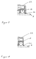
- the cover 22 is tightly attached to the carrier body 1 in an ultrasonic welding process (FIG. 8).
Landscapes
- Engineering & Computer Science (AREA)
- Power Engineering (AREA)
- Microelectronics & Electronic Packaging (AREA)
- Dc-Dc Converters (AREA)
- Coupling Device And Connection With Printed Circuit (AREA)
- Combinations Of Printed Boards (AREA)
- Multi-Conductor Connections (AREA)
- Connections Effected By Soldering, Adhesion, Or Permanent Deformation (AREA)
- Coils Or Transformers For Communication (AREA)
Abstract
Description
Es zeigt:
- Figur 1
- erste Ausführungsform der erfindungsgemäßen Lösung
- Figur 2
- zweite Ausführungsform der erfindungsgemäßen Lösung
- Figur 3
- Ausgestaltung des Transformatorkerns
- Figur 4
- Abschlußteil für die erfindungsgemäße Ausführung gemäß Figur 2
- Figur 5
- dritte Ausführung der erfindungsgemäßen Lösung
- Figur 6
- vierte Ausführungsform der erfindungsgemäßen Lösung
- Figur 7
- erste Abdichtung der elektrischen Vorrichtung
- Figur 8
- zweite Abdichtung der elektrischen Vorrichtung
Darüber hinaus weist der Kunststoffkörper 1 metallisierte und mit den Leiterbahnen 2 verbundene Kontaktöffnungen 6 und 7 auf, in welche Kontaktstifte 12 eingreifen, die auf einem Aluminiumträgerelement 8 angeordnet sind. Auf dem Trägerelement 8 sind eine Keramikleiterplatte 9 befestigt, welche Kupferbahnen 10 aufweist. Die Keramikleiterplatte 9 ist dabei beispielsweise auf den Aluminiumkörper 8 aufgeklebt. Die Kupferbahnen 10 stellen eine elektrische Verbindung zwischen den ebenfalls auf der Leiterplatte 9 angeordneten Leistungsbauelementen 11 und dem Kontaktstift 12 dar. Weiterhin ist auf dem Aluminiumträgerelement 8 das Unterteil 13 eines Planartransformators angeordnet.
Auch der Rand der Abdeckung 22 trägt eine Dichtung 23, auf welcher der Kunststoffträgerkörper 1 aufliegt. Somit werden mögliche Dichtigkeitsprobleme beim Anschluß an die Grundplatte durch die angespritzte Dichtlippe umgangen.
In Abwandlung der Vorrichtung gemäß Figur 5 ist die angespritzte Dichtung 20 am Trägerkörper zum Trägerelement 8 hin ausgebildet. Die Abdeckung 22 ist mit dem Trägerkörper 1 in einem Ultraschallschweißverfahren dicht befestigt.(Figur 8)
Claims (19)
- Kompakte elektrische Vorrichtung, insbesondere Schaltnetzteil, mit mindestens einer Induktivität und einer mit einer Bezugsspannung verbindbaren elektrischen Kontaktiereinrichtung, wobei die Induktivität mit der Kontaktiereinrichtung über eine erste elektrisch leitende Verbindung verbunden ist, dadurch gekennzeichnet, daß die Induktivität (3) und/oder die erste elektrisch leitende Verbindung (2) und/oder die Kontaktiereinrichtung (4, 5) in einem aus isolierendem Material bestehenden Trägerkörper (1) zumindest teilweise angeordnet sind und durch das Material des Trägerkörpers (1) gegeneinander isoliert sind, wobei eine, elektrische Schaltung (11) über eine zweite elektrische Verbindung (12) mit der ersten elektrischen Verbindung (2) des Trägerkörpers (1) verbunden ist.
- Kompakte elektrische Vorrichtung nach Anspruch 1 dadurch gekennzeichnet, dass zwei in dem Trägerkörper (1) angeordnete Induktivitäten als Transformator zur Angleichung verschiedener elektrischer Spannungen zwischen der elektrischen Schaltung (11) und der Kontaktiereinrichtung (4, 5) ausgebildet sind, wobei die ersten elektrischen Verbindungen (2) die Primärwicklung (3a) des Transformators mit der Kontaktiereinrichtung (4,5) und die Sekundärwicklung (3 b) des Transformators mit der elektrischen Schaltung (11) verbinden, wobei die Primär- (3a) und die Sekundärwicklung (3b) mindestens einen Teil eines Transformatorkerns (13) umschließen.
- Kompakte elektrische Vorrichtung, insbesondere Schaltnetzteil, mit einem Transformator zur Angleichung verschiedener elektrischer Spannungen zwischen einer elektrischen Schaltung und einer, mit einer Bezugsspannung verbindbaren elektrischen Kontaktiereinrichtung, wobei wenigstens eine Primärwicklung des Transformators mit der Kontaktiereinrichtung und wenigstens eine Sekundärwicklung des Transformators mit der elektrischen Schaltung über erste elektrische Verbindungen verbunden ist, wobei die Primär- und die Sekundärwicklung wenigstens einen Teil eines Transformatorkerns umschließen, dadurch gekennzeichnet, daß der Transformatorkern (15) und/oder die ersten elektrischen Verbindungen (2) und/oder die Kontaktiereinrichtung (4,5) in einem aus isolierendem Material bestehenden Trägerkörper (1) angeordnet sind, wobei die ersten elektrischen Verbindungen (2) durch das Material des Trägerkörpers (1) gegeneinander elektrisch isoliert sind und die Primär- und Sekundärwicklung (3) des Transformators (3a, 3b, 15) auf einem die elektrische Schaltung (11) tragenden, ebenen Trägerelement (8) so angeordnet sind, daß der Transformatorkern (15) von den Wicklungen (3a, 3b) umschlossen ist und eine zweite elektrische Verbindung (12) mit der ersten elektrischen Verbindung (2) des Trägerkörpers (1) verbunden ist.
- Kompakte elektrische Vorrichtung nach Anspruch 1 oder 3, dadurch gekennzeichnet, daß zur Bildung der zweiten elektrischen Verbindung mindestens ein Kontaktstift (12) auf einem Trägerelement (8) zur Verbindung der ebenfalls auf dem Trägerelement (8) angeordneten elektrischen Schaltung (11) mit einer der ersten elektrischen Verbindungen (2) des Trägerkörpers (1) angeordnet ist, welche in eine, mit der ersten elekrischen Verbindung (2) elektrisch verbundenen Öffnung (6,7) hineinragt.
- Kompakte elektrische Vorrichtung nach Anspruch 4, dadurch gekennzeichnet, daß der Kontaktstift (12) zur Herstellung der elektrischen Verbindung in die Öffnung (6, 7) des Trägerkörpers (1) eingepresst ist.
- Kompakte elektrische Vorrichtung nach Anspruch 4, dadurch gekennzeichnet, daß die Enden der als Leiterbahn (2) ausgebildeten ersten elektrischen Verbindung aus der Öffnung (6,7) des Trägerkörpers (1) diesen überragend hinausgeführt sind und der durch die Öffnung (6, 7) geführte Kontaktstift (12) gemeinsam mit den Enden der Leiterbahn (2) verlötet ist.
- Kompakte elektrische Vorrichtung nach Anspruch 6, dadurch gekennzeichnet, daß die Leiterbahnen (2) als Blechformteil ausgebildet sind.
- Kompakte elektrische Vorrichtung nach Anspruch 7, dadurch gekennzeichnet, daß die Blechformteile (2) aus dem Trägerkörper (1) zur Bildung der elektrischen Anschlüsse (4) der Kontaktiereinrichtung (4,5) herausgeführt sind, wobei der Körper (5) der Kontaktiereinrichtung (4,5) durch den Trägerkörper (1) gebildet ist.
- Kompakte elektrische Vorrichtung nach einem der vorhergehenden Ansprüche dadurch gekennzeichnet, dass der Trägerkörper (1) zur nachträglichen Aufnahme von weiteren elektrischen und/oder elektronischen Komponenten (30, 31, 32,) ausgebildet ist.
- Kompakte elektrische Vorrichtung nach Anspruch 9 dadurch gekennzeichnet, dass der Trägerkörper (1) eine mit Rasteinrichtungen versehene Aufnahme für eine weitere Komponente (33) aufweist.
- Kompakte elektrische Vorrichtung nach Anspruch 9 dadurch gekennzeichnet, dass außenseitig auf dem Trägerkörper (1) gehäuste oder ungehäuste elektronische Bauelemente (33) angeordnet sind.
- Kompakte elektrische Vorrichtung nach Anspruch 1 oder 3, dadurch gekennzeichnet, daß der Trägerkörper (1) Bestandteil eines Gehäuses ist, welches das die elektronische Schaltung (11) tragende Trägerelement (8) abdeckt.
- Kompakte elektrische Vorrichtung nach Anspruch 12, dadurch gekennzeichnet, daß der Trägerkörper (1) einen umlaufenden, abgewinkelten Kragen (19) aufweist, welcher auf dem Trägerelement (8) aufliegt, wobei an den Kragen (19) eine ebenfalls umlaufende Dichtung (20) angespritzt ist.
- Kompakte elektrische Vorrichtung nach Anspruch 12, dadurch gekennzeichnet, daß der Trägerkörper (1) als Gehäusemittelteil (24) mit einer einseitig angespritzten Dichtung (20) zur Auflage auf dem Trägerelement (8) ausgebildet ist, wobei das Gehäusemittelteil (24) mit einer planen Abdeckung (22) verschlossen ist, die ebenfalls eine angespritzte Dichtung (23) zur Auflage auf dem Gehäusemittelteil (24) aufweist.
- Kompakte elektrische Vorrichtung nach Anspruch 1 oder 3, dadurch gekennzeichnet, daß das Trägerelement (8) aus Metall, vorzugsweise Aluminium besteht und gleichzeitig zur Wärmeableitung für die Leistungsbauelemente (11) dient.
- Kompakte elektrische Vorrichtung nach Anspruch 15, dadurch gekennzeichnet, daß das Trägerelement (8) ein Substrat trägt, welches aus auf wärmeleitender Keramik (9) aufgebrachten Kupfer (10) besteht.
- Kompakte elektrische Vorrichtung nach Anspruch 2, dadurch gekennzeichnet, daß der Transformatorkern (13, 14) zweiteilig ausgebildet ist, wobei ein erstes, E-ähnliches Kernelement (13) auf dem Trägerelement (8) aufliegt, dessen drei senkrecht vom Trägerelement (8) wegweisenden Stege (13a, 13b, 13c) durch entsprechende Transformatoröffnungen des Trägerkörpers (1) greifen und ein zweites, eben oder E-ähnlich ausgebildetes Kernelement (14) die Stege (13a, 13b, 13c) abdeckt und magnetisch miteinander verbindet, wobei die Primär- und Sekundärwicklung (3a, 3b) umlaufend zwischen den Stegen (13a, 13b, 13c) angeordnet ist.
- Kompakte elektrische Vorrichtung nach Anspruch 2, dadurch gekennzeichnet, daß die Primär- und Sekundärwicklung (3a, 3b) des Transformators seitlich unterbrochen aus dem Trägerkörper (1) herausragen, wobei der, einen achtähnlichen Querschnitt aufweisende einstückige Transformatorkern (15), über die unterbrochenen Primär- und Sekundärwicklungen (3a, 3b) schiebbar ist, wobei nach Aufschieben des Transformatorkerns (15) die Primär- und Sekundärwicklung (3) mittels eines Trägerkörperabschlußteiles (18), welche den Wicklungen (3) angepaßte Leiterbahnen (29) enthält, elektrisch geschlossen werden.
- Kompakte elektrische Vorrichtung nach Anspruch 17 und 18, dadurch gekennzeichnet, daß die flächig ausgebildeten Primär- und Sekundärwicklungen (3a, 3b) des Transformators parallel zum ebenen Trägerelement (8) angeordnet sind.
Applications Claiming Priority (4)
| Application Number | Priority Date | Filing Date | Title |
|---|---|---|---|
| DE19943873 | 1999-09-14 | ||
| DE19943873 | 1999-09-14 | ||
| DE10039110 | 2000-08-07 | ||
| DE10039110A DE10039110A1 (de) | 1999-09-14 | 2000-08-07 | Kompakte elektrische Vorrichtung, insbesondere Schaltnetzteil |
Publications (3)
| Publication Number | Publication Date |
|---|---|
| EP1085793A2 true EP1085793A2 (de) | 2001-03-21 |
| EP1085793A3 EP1085793A3 (de) | 2001-11-21 |
| EP1085793B1 EP1085793B1 (de) | 2004-05-26 |
Family
ID=26006660
Family Applications (1)
| Application Number | Title | Priority Date | Filing Date |
|---|---|---|---|
| EP00118458A Expired - Lifetime EP1085793B1 (de) | 1999-09-14 | 2000-08-25 | Kompakte elektrische Vorrichtung, insbesondere Schaltnetzteil |
Country Status (3)
| Country | Link |
|---|---|
| US (1) | US6297981B1 (de) |
| EP (1) | EP1085793B1 (de) |
| JP (1) | JP2001135952A (de) |
Families Citing this family (11)
| Publication number | Priority date | Publication date | Assignee | Title |
|---|---|---|---|---|
| DE10113912B4 (de) * | 2001-03-21 | 2006-09-28 | Siemens Ag | Elektronische Vorrichtung |
| DE102008023714B4 (de) * | 2008-05-15 | 2011-01-20 | Semikron Elektronik Gmbh & Co. Kg | Anordnung mit einem Hauptträger und einer Leiterplatte mit Bauelementen |
| US11134580B2 (en) | 2010-07-08 | 2021-09-28 | Zagg Inc | Protective cover for portable electronic device and associated systems and methods |
| US20120008269A1 (en) * | 2010-07-08 | 2012-01-12 | David Gengler | Protective cover for a mobile computing device, systems including protective covers, and associated methods |
| WO2012178168A2 (en) | 2011-06-23 | 2012-12-27 | Zagg Intellectual Property Holding Co., Inc. | Accessory and support for electronic devices, systems including the same and methods |
| JP2015026820A (ja) * | 2013-06-18 | 2015-02-05 | 株式会社デンソー | 電子装置 |
| JP6447287B2 (ja) * | 2015-03-19 | 2019-01-09 | 株式会社明電舎 | 電力変換装置 |
| DE102016216207A1 (de) | 2016-08-29 | 2018-03-01 | Robert Bosch Gmbh | Verfahren zum Herstellen eines mikromechanischen Sensors |
| DE102016218207A1 (de) * | 2016-09-22 | 2018-03-22 | Robert Bosch Gmbh | Elektronische Baugruppe, insbesondere eine elektronische Leistungsbaugruppe für Hybridfahrzeuge oder Elektrofahrzeuge |
| DE102023201441A1 (de) * | 2023-02-20 | 2024-08-22 | Volkswagen Aktiengesellschaft | Antriebsvorrichtung für ein elektrisch betriebenes Fahrzeug |
| US20260104730A1 (en) * | 2024-10-15 | 2026-04-16 | Oxti Pte Ltd | Multifunctional carrying bag |
Family Cites Families (11)
| Publication number | Priority date | Publication date | Assignee | Title |
|---|---|---|---|---|
| US4943844A (en) * | 1985-11-22 | 1990-07-24 | Texas Instruments Incorporated | High-density package |
| US4903120A (en) * | 1985-11-22 | 1990-02-20 | Texas Instruments Incorporated | Chip carrier with interconnects on lid |
| US4800479A (en) * | 1988-03-31 | 1989-01-24 | Prime Computer, Inc. | High frequency power converter having compact output transformer, rectifier and choke |
| US5075821A (en) * | 1990-11-05 | 1991-12-24 | Ro Associates | DC to DC converter apparatus |
| EP0605712B1 (de) * | 1992-07-17 | 1999-09-08 | Vlt Corporation | Verpackung für elektronische komponenten |
| US5309130A (en) * | 1992-10-26 | 1994-05-03 | Pulse Engineering, Inc. | Self leaded surface mount coil lead form |
| US6091611A (en) * | 1994-04-26 | 2000-07-18 | Comarco Wireless Technologies, Inc. | Connectors adapted for controlling a small form factor power supply |
| US5835350A (en) * | 1996-12-23 | 1998-11-10 | Lucent Technologies Inc. | Encapsulated, board-mountable power supply and method of manufacture therefor |
| JPH10242913A (ja) * | 1997-02-24 | 1998-09-11 | Ando Electric Co Ltd | 光周波数安定化光源 |
| US5942795A (en) * | 1997-07-03 | 1999-08-24 | National Semiconductor Corporation | Leaded substrate carrier for integrated circuit device and leaded substrate carrier device assembly |
| US5973923A (en) * | 1998-05-28 | 1999-10-26 | Jitaru; Ionel | Packaging power converters |
-
2000
- 2000-08-25 EP EP00118458A patent/EP1085793B1/de not_active Expired - Lifetime
- 2000-09-06 US US09/656,301 patent/US6297981B1/en not_active Expired - Fee Related
- 2000-09-13 JP JP2000278823A patent/JP2001135952A/ja active Pending
Also Published As
| Publication number | Publication date |
|---|---|
| EP1085793B1 (de) | 2004-05-26 |
| JP2001135952A (ja) | 2001-05-18 |
| EP1085793A3 (de) | 2001-11-21 |
| US6297981B1 (en) | 2001-10-02 |
Similar Documents
| Publication | Publication Date | Title |
|---|---|---|
| EP1145610B1 (de) | Elektronisches steuergerät | |
| DE102008012570B4 (de) | Leistungshalbleitermodul-System, Leistungshalbleitermodulanordnung und Verfahren zur Herstellung einer Leistungshalbleitermodulanordnung | |
| DE4323827C1 (de) | Steckbare Baugruppe | |
| DE19756345C2 (de) | Anordnung zur Kontaktierung von Leiterplatten | |
| WO1997027728A2 (de) | Steuergerät, insbesondere für ein kraftfahrzeug | |
| WO2001017069A1 (de) | Steuergerät und lötverfahren | |
| EP0292848B1 (de) | Leistungshalbleitermodul und Verfahren zur Herstellung des Moduls | |
| EP1085793B1 (de) | Kompakte elektrische Vorrichtung, insbesondere Schaltnetzteil | |
| EP1814764B1 (de) | Elektronische vorrichtung | |
| EP1586223B1 (de) | Elektrisches verbindungselement, insbesondere für elektro wer kzeugschalter | |
| WO1993009656A1 (de) | Elektrisches gerät, insbesondere schalt- und steuergerät für kraftfahrzeuge | |
| DE69934659T2 (de) | Anordnung zum Zünden einer Entladungslampe und Herstellungsverfahren dafür | |
| EP1282345B1 (de) | Gehäuse zur Aufnahme einer Leiterplatte mit elektronischen Bauteilen in Fahrzeugen | |
| DE3527208A1 (de) | Elektrisches schaltgeraet | |
| DE2828146A1 (de) | Elektrische leiterplatte | |
| DE10340297A1 (de) | Schaltungsanordnung für aktive und passive elektrische und elektronische Bauelemente | |
| EP0709934B1 (de) | Datenübertragungssystem | |
| DE10039110A1 (de) | Kompakte elektrische Vorrichtung, insbesondere Schaltnetzteil | |
| DE102021111290A1 (de) | Motorgehäusedeckelanordnung eines Elektromotors mit von Formmasse umgebenden Bauteilen | |
| EP0275496A2 (de) | Anordnung zum elektrischen Anschluss eines Gerätes | |
| EP1085537A2 (de) | Planartransformator und Verfahren zur Herstellung seiner Wicklung sowie eine kompakte elektrische Vorrichtung mit einem solchen Planartransformator | |
| DE10039890A1 (de) | Planartransformator und Verfahren zur Herstellung seiner Wicklung sowie eine kompakte elektrische Vorrichtung mit einem solchen Planartransformator | |
| EP0857011B1 (de) | Elektrisches Gerät, insbesondere Schalt- und Steuergerät für Kraftfahrzeuge | |
| EP1070330B1 (de) | Leistungskondensator | |
| EP0798808A1 (de) | Anordnung zur Befestigung eines Kabelbaums an einer Trägerplatte |
Legal Events
| Date | Code | Title | Description |
|---|---|---|---|
| PUAI | Public reference made under article 153(3) epc to a published international application that has entered the european phase |
Free format text: ORIGINAL CODE: 0009012 |
|
| AK | Designated contracting states |
Kind code of ref document: A2 Designated state(s): AT BE CH CY DE DK ES FI FR GB GR IE IT LI LU MC NL PT SE Kind code of ref document: A2 Designated state(s): DE FR GB |
|
| AX | Request for extension of the european patent |
Free format text: AL;LT;LV;MK;RO;SI |
|
| PUAL | Search report despatched |
Free format text: ORIGINAL CODE: 0009013 |
|
| AK | Designated contracting states |
Kind code of ref document: A3 Designated state(s): AT BE CH CY DE DK ES FI FR GB GR IE IT LI LU MC NL PT SE |
|
| AX | Request for extension of the european patent |
Free format text: AL;LT;LV;MK;RO;SI |
|
| RAP1 | Party data changed (applicant data changed or rights of an application transferred) |
Owner name: SIEMENS AKTIENGESELLSCHAFT |
|
| 17P | Request for examination filed |
Effective date: 20011217 |
|
| AKX | Designation fees paid |
Free format text: DE FR GB |
|
| 17Q | First examination report despatched |
Effective date: 20030228 |
|
| GRAP | Despatch of communication of intention to grant a patent |
Free format text: ORIGINAL CODE: EPIDOSNIGR1 |
|
| GRAS | Grant fee paid |
Free format text: ORIGINAL CODE: EPIDOSNIGR3 |
|
| GRAA | (expected) grant |
Free format text: ORIGINAL CODE: 0009210 |
|
| AK | Designated contracting states |
Kind code of ref document: B1 Designated state(s): DE FR GB |
|
| REG | Reference to a national code |
Ref country code: GB Ref legal event code: FG4D Free format text: NOT ENGLISH |
|
| REF | Corresponds to: |
Ref document number: 50006576 Country of ref document: DE Date of ref document: 20040701 Kind code of ref document: P |
|
| PGFP | Annual fee paid to national office [announced via postgrant information from national office to epo] |
Ref country code: GB Payment date: 20040805 Year of fee payment: 5 |
|
| PGFP | Annual fee paid to national office [announced via postgrant information from national office to epo] |
Ref country code: FR Payment date: 20040817 Year of fee payment: 5 |
|
| GBT | Gb: translation of ep patent filed (gb section 77(6)(a)/1977) |
Effective date: 20040811 |
|
| PGFP | Annual fee paid to national office [announced via postgrant information from national office to epo] |
Ref country code: DE Payment date: 20041018 Year of fee payment: 5 |
|
| ET | Fr: translation filed | ||
| PLBE | No opposition filed within time limit |
Free format text: ORIGINAL CODE: 0009261 |
|
| STAA | Information on the status of an ep patent application or granted ep patent |
Free format text: STATUS: NO OPPOSITION FILED WITHIN TIME LIMIT |
|
| 26N | No opposition filed |
Effective date: 20050301 |
|
| PG25 | Lapsed in a contracting state [announced via postgrant information from national office to epo] |
Ref country code: GB Free format text: LAPSE BECAUSE OF NON-PAYMENT OF DUE FEES Effective date: 20050825 |
|
| PG25 | Lapsed in a contracting state [announced via postgrant information from national office to epo] |
Ref country code: DE Free format text: LAPSE BECAUSE OF NON-PAYMENT OF DUE FEES Effective date: 20060301 |
|
| GBPC | Gb: european patent ceased through non-payment of renewal fee |
Effective date: 20050825 |
|
| PG25 | Lapsed in a contracting state [announced via postgrant information from national office to epo] |
Ref country code: FR Free format text: LAPSE BECAUSE OF NON-PAYMENT OF DUE FEES Effective date: 20050831 |
|
| REG | Reference to a national code |
Ref country code: FR Ref legal event code: ST Effective date: 20111021 |