EP1085645A2 - Power supply circuit and optoelectronic device - Google Patents
Power supply circuit and optoelectronic device Download PDFInfo
- Publication number
- EP1085645A2 EP1085645A2 EP00308067A EP00308067A EP1085645A2 EP 1085645 A2 EP1085645 A2 EP 1085645A2 EP 00308067 A EP00308067 A EP 00308067A EP 00308067 A EP00308067 A EP 00308067A EP 1085645 A2 EP1085645 A2 EP 1085645A2
- Authority
- EP
- European Patent Office
- Prior art keywords
- voltage
- power supply
- supply circuit
- turned
- resistive
- Prior art date
- Legal status (The legal status is an assumption and is not a legal conclusion. Google has not performed a legal analysis and makes no representation as to the accuracy of the status listed.)
- Granted
Links
- 230000005693 optoelectronics Effects 0.000 title description 2
- 239000003990 capacitor Substances 0.000 claims abstract description 43
- 239000000758 substrate Substances 0.000 claims description 18
- 230000003139 buffering effect Effects 0.000 claims description 7
- 239000000463 material Substances 0.000 claims description 2
- 239000004973 liquid crystal related substance Substances 0.000 description 36
- 238000010586 diagram Methods 0.000 description 10
- 239000010408 film Substances 0.000 description 7
- 239000000470 constituent Substances 0.000 description 6
- 230000001747 exhibiting effect Effects 0.000 description 3
- 239000007788 liquid Substances 0.000 description 3
- 229910052751 metal Inorganic materials 0.000 description 3
- 239000002184 metal Substances 0.000 description 3
- 239000004988 Nematic liquid crystal Substances 0.000 description 2
- 239000011159 matrix material Substances 0.000 description 2
- 239000010409 thin film Substances 0.000 description 2
- XLOMVQKBTHCTTD-UHFFFAOYSA-N Zinc monoxide Chemical compound [Zn]=O XLOMVQKBTHCTTD-UHFFFAOYSA-N 0.000 description 1
- 230000006978 adaptation Effects 0.000 description 1
- 229910052782 aluminium Inorganic materials 0.000 description 1
- XAGFODPZIPBFFR-UHFFFAOYSA-N aluminium Chemical compound [Al] XAGFODPZIPBFFR-UHFFFAOYSA-N 0.000 description 1
- 230000003321 amplification Effects 0.000 description 1
- 238000007743 anodising Methods 0.000 description 1
- 230000003247 decreasing effect Effects 0.000 description 1
- 230000003292 diminished effect Effects 0.000 description 1
- 239000012212 insulator Substances 0.000 description 1
- 238000003199 nucleic acid amplification method Methods 0.000 description 1
- 229920000642 polymer Polymers 0.000 description 1
- 230000001681 protective effect Effects 0.000 description 1
- 239000000565 sealant Substances 0.000 description 1
- 125000006850 spacer group Chemical group 0.000 description 1
- 230000007704 transition Effects 0.000 description 1
Images



Classifications
-
- H—ELECTRICITY
- H02—GENERATION; CONVERSION OR DISTRIBUTION OF ELECTRIC POWER
- H02M—APPARATUS FOR CONVERSION BETWEEN AC AND AC, BETWEEN AC AND DC, OR BETWEEN DC AND DC, AND FOR USE WITH MAINS OR SIMILAR POWER SUPPLY SYSTEMS; CONVERSION OF DC OR AC INPUT POWER INTO SURGE OUTPUT POWER; CONTROL OR REGULATION THEREOF
- H02M3/00—Conversion of DC power input into DC power output
- H02M3/02—Conversion of DC power input into DC power output without intermediate conversion into AC
- H02M3/04—Conversion of DC power input into DC power output without intermediate conversion into AC by static converters
- H02M3/10—Conversion of DC power input into DC power output without intermediate conversion into AC by static converters using discharge tubes with control electrode or semiconductor devices with control electrode
- H02M3/145—Conversion of DC power input into DC power output without intermediate conversion into AC by static converters using discharge tubes with control electrode or semiconductor devices with control electrode using devices of a triode or transistor type requiring continuous application of a control signal
- H02M3/155—Conversion of DC power input into DC power output without intermediate conversion into AC by static converters using discharge tubes with control electrode or semiconductor devices with control electrode using devices of a triode or transistor type requiring continuous application of a control signal using semiconductor devices only
- H02M3/156—Conversion of DC power input into DC power output without intermediate conversion into AC by static converters using discharge tubes with control electrode or semiconductor devices with control electrode using devices of a triode or transistor type requiring continuous application of a control signal using semiconductor devices only with automatic control of output voltage or current, e.g. switching regulators
-
- H—ELECTRICITY
- H02—GENERATION; CONVERSION OR DISTRIBUTION OF ELECTRIC POWER
- H02M—APPARATUS FOR CONVERSION BETWEEN AC AND AC, BETWEEN AC AND DC, OR BETWEEN DC AND DC, AND FOR USE WITH MAINS OR SIMILAR POWER SUPPLY SYSTEMS; CONVERSION OF DC OR AC INPUT POWER INTO SURGE OUTPUT POWER; CONTROL OR REGULATION THEREOF
- H02M1/00—Details of apparatus for conversion
- H02M1/0048—Circuits or arrangements for reducing losses
-
- Y—GENERAL TAGGING OF NEW TECHNOLOGICAL DEVELOPMENTS; GENERAL TAGGING OF CROSS-SECTIONAL TECHNOLOGIES SPANNING OVER SEVERAL SECTIONS OF THE IPC; TECHNICAL SUBJECTS COVERED BY FORMER USPC CROSS-REFERENCE ART COLLECTIONS [XRACs] AND DIGESTS
- Y02—TECHNOLOGIES OR APPLICATIONS FOR MITIGATION OR ADAPTATION AGAINST CLIMATE CHANGE
- Y02B—CLIMATE CHANGE MITIGATION TECHNOLOGIES RELATED TO BUILDINGS, e.g. HOUSING, HOUSE APPLIANCES OR RELATED END-USER APPLICATIONS
- Y02B70/00—Technologies for an efficient end-user side electric power management and consumption
- Y02B70/10—Technologies improving the efficiency by using switched-mode power supplies [SMPS], i.e. efficient power electronics conversion e.g. power factor correction or reduction of losses in power supplies or efficient standby modes
Definitions
- the present invention relates to a power supply circuit for feeding power with a small loss and an electro-optical device to which power is fed using the power supply circuit and which is characterized by low power consumption.
- a conventional power supply circuit for example, a power supply circuit for producing a high voltage Vout from a low voltage Vin and supplying the high voltage Vout.
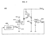
- Fig. 9 is a block diagram showing the circuitry of a conventional power supply circuit 400.
- a switch 412 is realized with a transistor in practice, and turned on when a signal CTR that is a gate signal is driven high.
- One terminal of the switch 412 is connected to a line, over which the voltage Vin is applied, via an inductor (coil) 414.
- the other terminal thereof is connected to a ground line over which a reference potential GND is applied.
- One terminal of the switch 412 is connected to one terminal of a capacitor 418 through the conduction in a forward direction of a diode 416. Consequently, a held voltage is output as the voltage Vout.
- the other terminal of the capacitor 418 is connected to the ground line.
- the output voltage Vout developed at one terminal of the capacitor 418 has a fraction thereof developed due to resistors 420 and 422.
- the fractional voltage is applied to a negative input terminal of a comparator 424.
- a voltage to be applied to the negative input terminal of the comparator 424 shall be a voltage Vout'.
- a reference voltage Vref is applied to a positive input terminal of the comparator 424.
- an output signal CMP of the comparator 424 is, as shown in Fig. 10, driven high.
- the output signal CMP is driven low.
- a control circuit 426 outputs, as shown in Fig. 10, a pulsating signal CTR having a certain pulse width W.
- the switch 412 is turned on. This causes a current Ion to flow from the line, over which the voltage Vin is applied, through the inductor 414 towards the ground line. Energy is accumulated in the inductor. When the switch 412 is turned off, an off current Ioff flows through the inductor 414. The accumulated energy is added to the voltage Vin through the conduction in the forward direction of the diode 416 according to the series feed. The energy thus moves to the capacitor 418. When the energy accumulated in the inductor 414 has entirely moved to the capacitor 418, the diode 416 is inversely biased. It will therefore not take place that the energy accumulated in the capacitor 418 flows backward through the diode 416.
- the output voltage Vout drops gradually according to the magnitude of a load.
- the output signal CMP of the comparator 424 makes a low-to-high transition. This causes the control circuit 426 to output the pulsating signal CTR.
- the switch 412 is then turned on. After energy is accumulated in the inductor 414, the switch 412 is turned off. The energy moves to the capacitor 418. Consequently, the output voltage Vout rises. In other words, when the voltage Vout' falls below the reference voltage Vref, control is given to raise the output voltage Vout.
- the voltage Vout' may exceed the reference voltage Vref.
- the output signal CMP of the comparator 424 remains low.
- the switch 412 is not therefore turned on or off.
- the capacitor 418 discharges according to a load. Consequently, the output voltage Vout drops gradually. In other words, when the voltage Vout' exceeds the reference voltage Vref, the discharge of the capacitor 418 causes control to be given for lowering the output voltage Vout.
- the output voltage Vout is stabilized when control given for raising the output voltage Vout and a control given for lowering it are balanced, that is, when the voltage Vout' becomes equal to the reference voltage Vref.
- a voltage "Vin-GND” that has not been boosted should be used as a supply voltage to be applied to the control circuit 426 and comparator 424.
- the voltage Vout' and reference voltage Vref with which the voltage is compared must fall below “Vin-GND.”
- the voltage "Vin-GND” is used as the supply voltage to be applied to the comparator 424 in an effort to realize simple circuitry, the voltage must not be compared directly with the boosted voltage Vout. Namely, a lower voltage (fractional voltage) produced by stepping down the voltage Vout must be used as a voltage with which the voltage "Vin-GND" is compared.
- An object of the present invention is to provide a power supply circuit capable of minimizing power consumption and contributing to a compact and simple design, and to also provide an electro-optical device using the power supply circuit.
- a power supply circuit for converting a first voltage that is an input voltage into a second voltage that is an output voltage and outputting the second voltage.
- the power supply circuit has two or more resistive elements, a pair of first switching elements, and a holding element.
- the two or more resistive elements cause a fraction of the second voltage to develop.
- the pair of first switching elements is turned on or off in order to enable or disable flow of a current through the two or more resistive elements.
- the holding element holds the fractional voltage developed due to the resistive elements.
- the power supply circuit is characterized in that control is given so that the voltage held by the holding element will be equal to a reference voltage.
- the first voltage is supplied over a first line and a ground line, while the second voltage is supplied over a second line and the ground line.
- the resistive elements include a first resistive element connected to the second line and a second resistive element connected to the ground line.
- the first resistive element and second resistor are connected in series with each other.
- the holding element is preferably composed of a first capacitor interposed between a fractional voltage point, at which the first and second resistive elements cause a fractional voltage to develop, and the second line, and a second capacitor interposed between the fractional voltage point and the ground line.
- a ratio of the resistance of the first resistive element to that of the second resistive element is, preferably, substantially equal to a ratio of the capacitance of the second capacitor to that of the first capacitor.
- a relatively long period of time is required until the voltage held by the holding element agrees with a fractional voltage developed due to the resistive elements. This is attributable to the resistances of the resistive elements and the capacitance of the holding element.
- the pair of first switching elements must be on during the period. When the pair of first switching elements is turned on, a current flows through the resistive elements. This is undesirable in terms of low power consumption.
- a buffer for buffering a voltage at the fractional voltage point should preferably be interposed between the fractional voltage point, at which a fractional voltage is developed due to the resistive elements, and the holding device.
- a second switching element should preferably be interposed between the buffer and the holding element.
- the second switching element is turned on after or at the same time when the pair of first switching elements is turned on.
- the second switching element is turned off before or at the same time when the pair of first switching elements is turned off. Owing to this constituent feature, it can be prevented that the buffer outputs an unstable voltage immediately after the pair of first switching elements is turned on.
- the buffer is preferably disabled from buffering data during at least the period during which the pair of first switching elements is off. Owing to this constituent feature, since an unnecessary action of the buffer is omitted, a consumed current can be suppressed further.
- an electro-optical device having a plurality of pixels realized with an electro-optical material sandwiched between two opposed substrates.
- the electro-optical device has a drive circuit for feeding a driving signal, which is used to drive the plurality of pixels, and a power supply circuit for converting a first voltage into a second voltage and applying the second voltage so as to power the drive circuit.
- the power supply circuit has two or more resistive elements, a pair of first switching elements, and a holding element. The two or more resistive elements cause a fraction of the second voltage to develop.
- the pair of first switching elements is turned on or off in order to enable or disable flow of a current through the two or more resistive elements.
- the holding element holds the fractional voltage developed due to the resistive elements. Owing to these constituent features, when the pair of first switching elements is turned off, no current flows. Consequently, a loss in power caused by the resistive elements can be suppressed. Moreover, the resistive elements need not exhibit a high resistance. This contributes to a compact and simple design. Besides, the power supply circuit does not become susceptible to noise. Furthermore, since the fractional voltage of the second voltage is held in the holding element, the second voltage is output while stabilized.
- Fig. 1 is a block diagram showing the circuitry of a power supply circuit in accordance with a first embodiment of the present invention.
- Fig. 2 is a timing chart for explaining the action of the power supply circuit of figure 1.
- Fig. 3 is a block diagram showing the circuitry of a power supply circuit in accordance with a second embodiment of the present invention.
- Fig. 4 is a timing chart for explaining the action of the power supply circuit of figure 3.
- Fig. 5 is a block diagram showing the circuitry of a power supply circuit in accordance with a third embodiment of the present invention.
- Fig. 6 is a timing chart for explaining the action of the power supply circuit of figure 5.
- Fig. 7 is a block diagram showing the electrical configuration of a liquid crystal display device that is an example of an electro-optical device in accordance with a fourth embodiment of the present invention.
- Fig. 8 is a cutaway perspective view showing the structure of a major portion of a liquid crystal panel of the liquid crystal display device of figure 7.
- Fig. 9 is a block diagram showing the circuitry of a conventional power supply circuit.
- Fig. 10 is a timing chart for explaining the action of the conventional power supply circuit.
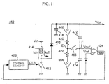
- Fig. 1 is a block diagram showing the circuitry of a power supply circuit in accordance with the present embodiment.
- An illustrated power supply circuit 450 is different from the conventional power supply circuit 400 in a point that switches 462, 464, and 466 and capacitors 472 and 474 are newly included.
- the switch 462 is interposed between one terminal of the capacitor 418 which serves as an output terminal and the resistor 420.
- the switch 464 is interposed between the ground line over which the reference potential GND is applied and the resistor 422.
- the switch 466 is interposed between point E, which is the fractional voltage point at which a fractional voltage is developed due to the resistors 420 and 422, and point F that is the negative input terminal of the comparator 424.
- the capacitor 472 is interposed between point F and one terminal of the capacitor 418 that serves as the output terminal.
- the capacitor 474 is interposed between point F and the ground line.
- the resistances of the resistors 420 and 422 are R1 and R2 and the capacitances of the capacitors 472 and 474 are C1 and C2.
- the switches 462, 464, and 466 are controlled to be turned on or off by means of a circuit that is not shown.
- Fig. 2 is a timing chart for explaining the action. As illustrated, the switches 462, 464, and 466 are repeatedly turned on or off all together at intervals of a cycle determined in consideration of a leakage caused by the comparator 424.
- the switches 462, 464, and 466 are turned off.
- the potential at point E becomes unstable.
- the potential at point F remains the same as the potential at point E attained by the capacitors 472 and 474 immediately before the switches are turned off.
- the output voltage Vout varies because power is consumed by a load and the switch 412 is turned on or off.
- point F is connected to the output terminal via the capacitor 472 and also connected to the ground line via the capacitor 474. Therefore, the potential at point F becomes equal to a fraction of the output voltage Vout developed based on the ratio of the capacitance of the capacitor 472 to that of the capacitor 474.
- the power supply circuit 450 no current flows through the resistors 420 and 422 during a period during which the switches 462 and 464 are off. A loss in power caused by the resistors can be suppressed.
- the resistors 420 and 422 need not exhibit a high resistance. This contributes to a compact and simple design. Moreover, the power supply circuit does not become susceptible to noise. Furthermore, even during a period during which the switches 462 and 464 are off, the potential at point F that is the negative input terminal of the comparator 424 nearly agrees with that at point E attained during a period during which the switches 462 and 464 are on. Stable output of the output voltage Vout will not be interrupted.
- the switches 462, 464, and 466 are repeatedly turned on and off at intervals of a certain cycle.
- the switches may be turned on and off irregularly. If a leakage caused by the comparator 424 is small enough, an off period may be extended.
- the potential at point E to be attained immediately after the switches 462 and 464 are turned on varies depending on the time constant of a floating capacitance relative to the resistances of the resistors 420 and 422.
- the switches 462, 464, and 466 are supposed to be turned on or off all together. Either of the switches 462 and 464 may be turned off earlier than the switch 466 because of a difference in the switching ability of one switch from another. In this case, a current leaks out of the capacitors 472 and 474 via the other switches. A holding voltage therefore varies.
- the switch 466 should preferably be designed so that, as indicated in parentheses in Fig. 2, it will be turned on after the switches 462 and 464 are turned on and it will be turned off before the switches 462 and 464 are turned off.
- the switch 462 is connected near the line over which the voltage Vin is supplied, and the switch 464 is connected near the ground line.
- the switches 462 and 464 may be connected near point E that is the fractional voltage point at which a fractional voltage is developed due to the resistors 420 and 422.
- Fig. 3 is a block diagram showing the circuitry of a power supply circuit in accordance with the present embodiment.
- An illustrated power supply circuit 452 is different from the power supply circuit 450 in accordance with the first embodiment (see Fig. 1) in a point that the capacitor 474 interposed between point F and the ground line is excluded. In this circuitry, one capacitor can be excluded.
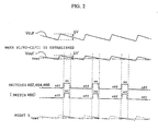
- the voltage at point F developed during a period during which the switches 462, 464, and 466 are off varies, as shown in Fig. 4, within the same variation width ⁇ V as the voltage Vout does. The voltage at point F therefore disagrees with the voltage at point E developed during a period during which the switches 462 and 464 are on.
- the voltage Vout' at point F with which the comparator 424 compares a voltage contains an error equivalent to the width ⁇ V. This is undesirable in terms of stable output. Specifically, assuming that the variation width of the output voltage Vout is ⁇ V, a variation width of the voltage at point E is expressed as ⁇ V ⁇ R2/(R1+R2) because of the resistors 420 and 422 due to which a fractional voltage is developed. However, point F is connected to the output terminal via the capacitor 472 alone. As long as the switches 462, 464, and 466 are off, the voltage Vout' varies within the same variation width ⁇ V as the output voltage Vout does.
- a difference between a fractional voltage of the output voltage Vout produced due to the resistors 420 and 422 and the voltage Vout' at point F developed when the switch 466 is off is diminished when the latter voltage Vout' is close to the reference voltage Vref.
- the switches 462, 464, and 466 are therefore turned on when, as shown in Fig. 4, the voltage Vout' at point F falls below the reference voltage Vref and energy from the inductor 414 moves to the capacitor 418 to thus boost the voltage at the capacitor 418. More particularly, the switches are turned on when the output signal CMP of the comparator 424 is high and the control signal CTR output from the control circuit 426 is high.
- the variation width of the output voltage Vout agrees with that of the voltage at point F as long as the switches 462, 464, and 466 are off. Therefore, even when the ratio of the output voltage Vout resulting from boosting to the voltage Vin is high and the resistance R1 of the resistor 420 is higher than the resistance R2 of the resistor 422, a gain to be produced by the comparator 424 can be decreased. Consequently, the power supply circuit can act on a stable basis. This leads to lower power consumption.
- an on period during which the switches 462, 464, and 466 are on must be long enough. This is because consideration must be taken into the time constants of the capacitances C1 and C2 of the capacitors 472 and 474 and the floating capacitance relative to the resistances R1 and R2 of the resistors 420 and 422. However, when the on period during which the switches 462 and 464 are on is extended, a larger current flows through the resistors 420 and 422. This is undesirable in terms of low power consumption.
- FIG. 5 is a block diagram showing the circuitry of a power supply circuit in accordance with the present embodiment.
- An illustrated power supply circuit 454 is different from the power supply circuit 450 in accordance with the first embodiment (see Fig. 1) in a point that a buffer 478 and a switch 468 are interposed between the switch 466 and point F.
- the buffer 478 amplifies a signal at an amplification factor 1 without reversing the polarity of the signal (buffering) only when an enabling signal ENB is high.
- an input impedance offered by a buffer is higher than an output impedance offered thereby.
- the potential at point F can therefore be agreed with that at point E immediately.
- the on period during which the switches 462, 464, and 466 are on can be made shorter than the on period set according to the first and second embodiments. Accordingly, power to be consumed by the resistors 420 and 422 can be suppressed.
- the switch 468 is turned on after the switches 462, 464, and 466 are turned on, and turned off after the switches 462, 464, and 466 are turned off. It can therefore be prevented that the potential at point E that is unstable immediately after the switches 462, 464, and 466 are turned on is applied to point F serving as the negative input terminal of the comparator 424. In this circuitry, the on-off timing of the switches 462, 464, and 466 need not be agreed with one another.
- the switch 466 may be turned on after the switches 462 and 464 are turned on and before the switch 468 is turned on.
- the switch 466 may be turned off before the switches 462 and 464 are turned off and after the switch 468 is turned on.
- Buffering must be performed using the buffer 478 only during a period during which the switch 466 is on.
- the action of buffering is therefore enabled only during that period.
- the action speed of the buffer may become critical. For this reason, as shown in Fig. 6, the enabling signal ENB is driven high for only a period during which the switches 462, 464, and 466 are on.
- the action of buffering is enabled during that period.
- the action should preferably be performed during a period of time longer than a required time.
- the capacitor 474 in the power supply circuit 454 in accordance with the third embodiment may be excluded similarly to that in the power supply circuit 452 in accordance with the second embodiment.
- a protective diode may be connected to the input terminal of the buffer 478 if necessary.
- the actions of the power supply circuits in accordance with the aforesaid embodiments have been described in relation mainly to a steady state in which the output voltage Vout is stabilized.
- the switches 462, 464, 466, and 468 are turned on or off cyclically or irregularly. Alternatively, the switches may be held on immediately after power is fed, that is, until the output voltage Vout is produced by boosting the voltage Vin up to the specific voltage. Once the voltage Vin has reached the specific voltage, the switches may be started to be turned on or off.
- the aforesaid embodiments are implemented in a step-up power supply circuit.
- an inverting power supply circuit for inverting the polarity of an input voltage and outputting a reverse voltage or a step-down power supply circuit for outputting a voltage lower than an input voltage will do.
- the liquid crystal display device is an example of an electro-optical device.
- the aforesaid power supply circuit 450, 452, or 454 is adapted to the liquid crystal display device.
- Fig. 7 is a block diagram showing the electrical configuration of the liquid crystal display device.
- 160 data lines 212 are formed in columns (in a Y direction) in a liquid crystal panel 100, and 200 scanning lines 312 are formed in rows (in an X direction) therein.
- Pixels 116 are formed at intersections between the data lines 212 and scanning lines 312.
- the pixels 116 are each realized by connecting a liquid crystal display element (liquid crystal layer) 118 in series with a thin film diode (TFD) 220.
- TDD thin film diode
- Fig. 8 is a partially cutaway perspective view illustratively showing the structure.
- the liquid crystal panel 100 consists of an element substrate 200 and an opposed substrate 300 opposed to the element substrate 200.
- a plurality of pixel electrodes 234 is arranged in the form of a matrix on an opposed surface of the element substrate 200 that is opposed to the opposed substrate 300.
- Pixel electrodes 234 arranged in a column are connected to one data line 212, which extends in a column like a rectangular piece, via the TFDs 220.
- the TFD 220 is composed of a first metallic film 222, an oxide film 224 produced by anodizing the first metallic film 222, and a second metallic film 226 when viewed from the substrate, and has a metal/dielectric/metal sandwich structure.
- the TFD 220 thus exhibits the same switching characteristic in both positive and negative directions as a diode switch.
- the scanning lines 312 extend in rows orthogonal to the data lines 212, and are arranged to serve as electrodes opposed to the pixel electrodes 234.
- the thus-formed element substrate 200 and opposed substrate 300 are separated from each other with a certain distance held between them owing to a sealant (not shown) applied to the margins of the substrates and a spacer (not shown) scattered appropriately.
- the closed space is filled with a twisted nematic liquid crystal 105, whereby the liquid crystal layers 118 shown in Fig. 7 are formed.
- the liquid crystal layer 118 at each intersection between the data line 212 and scanning line 312 is composed of the scanning line 312, pixel electrode 234, and liquid crystal 105 lying between the scanning line 312 and pixel electrode 234.
- color filters arranged in the form of a stripe, mosaic, or triangle may be attached to the opposed substrate 300 according to the usage of the liquid crystal panel 100.
- a black matrix screen for intercepting light may be formed to cover a portion other than the portion of the opposed substrate 300 occupied by the color filters.
- an orientation film rubbed in a predetermined direction is placed on each of the opposed surfaces of the element substrate 200 and opposed substrate 300.
- a polarizer whose property is determined with a direction in which liquid crystalline molecules are aligned is placed on each of the backs of the substrates (not shown).
- the aforesaid orientation film and polarizer are unnecessary. This leads to higher light utility.
- the adaptation of the polymeric liquid crystal is advantageous in terms of high brightness and low power consumption characterizing the liquid crystal panel 100.
- the pixel electrodes 234 may be formed with a metallic film exhibiting a high reflectance, such as, aluminum.
- a super homeotropic liquid crystal having liquid crystalline molecules aligned nearly perpendicularly with no voltage applied may be adopted.
- the TFD 220 is an example of a two-terminal nonlinear element.
- a zinc oxide (ZnO) varistor an element produced using a metal semi-insulator (MSI), or an element produced by connecting these two elements in series or parallel with each other in opposite directions will do.
- ZnO zinc oxide
- MSI metal semi-insulator
- an X driver 250 is generally called a data line drive circuit.
- the X driver 250 supplies data signals X1 to X160 to the respective data lines 212 according to the contents of display data.
- the voltage of the data signal is defined with either of the voltages Vin and GND.
- a Y driver 350 is generally called a scanning line drive circuit.
- the Y driver 350 selects the scanning lines 312 one by one, and applies a selection voltage V1 or V2 to a scanning line 312 during a selected period during which the scanning line 312 is sequentially selected.
- the Y driver 350 applies a non-selection voltage Vin or GND to scanning lines during an unselected period during which the scanning lines are unselected.
- a power supply circuit 450 boosts a single supply voltage "Vin-GND” to produce the selection voltage V1 of positive polarity.
- the power supply circuit 450 inverts the polarity of the voltage V1 using an intermediate value of the voltage "Vin-GND” as a reference value, and thus produces the selection voltage V2 of negative polarity.
- the voltages Vin and GND are used as a non-selection voltage of positive polarity and a non-selection voltage of negative polarity as they are.
- TFDs 220 become conducting.
- the data signals are applied to the TFDs 220 over the data lines 212. Consequently, predetermined charge is accumulated in the liquid crystal layers 118 connected to the TFDs 220.
- the non-selection voltage Vin is applied to the TFDs 220. This causes the TFDs 220 to become nonconducting. Nevertheless, if the TFDs 220 causes a little leakage (off leakage) and the liquid crystal layers 118 provide sufficiently high resistance, the charges accumulated in the liquid crystal layers 118 are held intact.
- each TFD 220 is driven alternately with voltages of opposite polarities in order to control an amount of charge to be accumulated. Consequently, the aligned state of liquid crystalline molecules varies depending on each pixel. Eventually, predetermined information can be displayed.
- the liquid crystal panel 100 has been described by taking for instance a liquid crystal panel having the TFDs 220.
- the present invention is not limited to this type of liquid crystal panel.
- a liquid crystal panel having thin film transistors (TFTs) will do.
- TFTs thin film transistors
- scanning lines and data lines are formed on one substrate, and the TFTs located at the intersections between the scanning lines and data lines have the gates thereof connected to the scanning lines and the sources thereof connected to the data lines.
- the present invention can be implemented in a passive liquid crystal panel having no switching element but including a super twisted nematic liquid crystal.
- the present invention can be implemented in an electroluminescent display device having luminescent layers arranged instead of the liquid crystal layers, or any other electro-optical device for displaying data using various electro-optical effects.
- a current does not always flow through resistive elements.
- a loss in power caused by the resistive elements can therefore be suppressed.
- the resistive elements need not exhibit a high resistance. This contributes to a compact and simple design.
- a power supply circuit does not become susceptible to noise.
Landscapes
- Engineering & Computer Science (AREA)
- Power Engineering (AREA)
- Liquid Crystal Display Device Control (AREA)
- Control Of Indicators Other Than Cathode Ray Tubes (AREA)
- Liquid Crystal (AREA)
Abstract
Description
Claims (7)
- A power supply circuit for converting a first voltage that is an input voltage into a second voltage that is an output voltage, and outputting said second voltage, comprising:wherein control is given so that the voltage held by said holding element is equal to a reference voltage.two or more resistive elements for causing a fraction of said second voltage to develop;a pair of first switching elements to be turned on or off in order to enable or disable flow of a current through said two or more resistive elements; anda holding element for, when said pair of first switching elements is turned on, holding the fractional voltage developed due to said resistive elements,
- A power supply circuit according to claim 1, wherein: said first voltage is applied over a first line and a ground line, and said second voltage is applied over a second line and said ground line; said resistive elements include a first resistive element connected to said second line and a second resistive element connected to said ground line, said first resistive element and said second resistive element are serially connected with each other; and said holding element consists of a first capacitor interposed between a fractional voltage point, at which said fractional voltage is developed due to said first and second resistive elements, and said second line, and a second capacitor interposed between said fractional voltage point and said ground line.
- A power supply circuit according to claim 2, wherein the ratio of the resistance of said first resistive element to that of said second resistive element is substantially equal to the ratio of the capacitance of said second capacitor to that of said first capacitor.
- A power supply circuit according to claim 1, further comprising a buffer interposed between said fractional voltage point, at which said fractional voltage is developed due to said resistive elements, and said holding element, and used to buffer said voltage at said fractional voltage point.
- A power supply circuit according to claim 4, further comprising a second switching element interposed between said buffer and said holding element, turned on after or at the same time when said pair of first switching elements is turned on, and turned off before or at the same time when said pair of first switching elements is turned off.
- A power supply circuit according to claim 4, wherein said buffer is disabled from buffering a signal during at least a period during which said pair of first switching elements is off.
- An electro-optical device having a plurality of pixels realized with an electro-optical material sandwiched between two mutually opposed substrates, comprising:wherein control is given so that the voltage held by said holding element is equal to a reference voltage.a drive circuit for applying a driving signal used to drive said plurality of pixels; anda power supply circuit for converting a first voltage into a second voltage and applying the second voltage to power said drive circuit, said power supply circuit comprising: two or more resistive elements for causing a fraction of said second voltage to develop; a pair of first switching elements to be turned on or off in order to enable or disable flow of a current through said two or more resistive elements; and a holding element for, which said pair of first switching elements is turned on, holding the fractional voltage developed due to said resistive elements,
Applications Claiming Priority (2)
| Application Number | Priority Date | Filing Date | Title |
|---|---|---|---|
| JP26266299 | 1999-09-16 | ||
| JP26266299A JP3726584B2 (en) | 1999-09-16 | 1999-09-16 | Power supply circuit and electro-optical device |
Publications (3)
| Publication Number | Publication Date |
|---|---|
| EP1085645A2 true EP1085645A2 (en) | 2001-03-21 |
| EP1085645A3 EP1085645A3 (en) | 2003-01-29 |
| EP1085645B1 EP1085645B1 (en) | 2010-02-10 |
Family
ID=17378887
Family Applications (1)
| Application Number | Title | Priority Date | Filing Date |
|---|---|---|---|
| EP00308067A Expired - Lifetime EP1085645B1 (en) | 1999-09-16 | 2000-09-15 | Power supply circuit and optoelectronic device |
Country Status (6)
| Country | Link |
|---|---|
| US (1) | US6297622B1 (en) |
| EP (1) | EP1085645B1 (en) |
| JP (1) | JP3726584B2 (en) |
| CN (1) | CN1149428C (en) |
| DE (1) | DE60043803D1 (en) |
| TW (1) | TW573163B (en) |
Families Citing this family (14)
| Publication number | Priority date | Publication date | Assignee | Title |
|---|---|---|---|---|
| US6208121B1 (en) * | 1998-01-20 | 2001-03-27 | Iap Research, Inc. | Switching power supply with AC waveform capability |
| JP2001282164A (en) * | 2000-03-31 | 2001-10-12 | Sanyo Electric Co Ltd | Driving device for display device |
| US6583580B2 (en) * | 2000-07-07 | 2003-06-24 | Seiko Epson Corporation | EL element driving circuit and method, and electronic apparatus |
| JP2005135031A (en) * | 2003-10-28 | 2005-05-26 | Sanyo Electric Co Ltd | Power supply circuit |
| JP2005137066A (en) * | 2003-10-28 | 2005-05-26 | Sanyo Electric Co Ltd | Power source circuit |
| JP4352937B2 (en) * | 2004-03-03 | 2009-10-28 | セイコーエプソン株式会社 | Power supply circuit, electro-optical device and electronic apparatus |
| JP4075830B2 (en) * | 2004-03-12 | 2008-04-16 | セイコーエプソン株式会社 | Power supply circuit and driver IC, liquid crystal display device and electronic apparatus using the same |
| US7173285B2 (en) * | 2004-03-18 | 2007-02-06 | Cree, Inc. | Lithographic methods to reduce stacking fault nucleation sites |
| US8604757B2 (en) * | 2010-02-01 | 2013-12-10 | Mitsubishi Electric Corporation | DC/DC power conversion apparatus |
| CN103991366A (en) * | 2013-02-17 | 2014-08-20 | 法国圣戈班玻璃公司 | Sun shading device, vehicle and glass sun shading method |
| JP6560360B2 (en) * | 2015-04-17 | 2019-08-14 | ライオン セミコンダクター インク. | Asymmetric switching capacitor regulator |
| JP6660241B2 (en) * | 2016-04-25 | 2020-03-11 | エイブリック株式会社 | Reference voltage generation circuit and DCDC converter having the same |
| US10637353B2 (en) * | 2016-11-30 | 2020-04-28 | Dialog Semiconductor (Uk) Limited | Feedback voltage DC level cancelling for configurable output DC-DC switching converters |
| CN115912899B (en) * | 2023-02-20 | 2023-05-23 | 广东东菱电源科技有限公司 | Capacitor series voltage dividing circuit |
Family Cites Families (16)
| Publication number | Priority date | Publication date | Assignee | Title |
|---|---|---|---|---|
| US3736496A (en) * | 1971-12-13 | 1973-05-29 | Rca Corp | Energy pump voltage regulator |
| BE883739A (en) * | 1980-06-10 | 1980-10-01 | Organisation Europ De Rech S S | DEVICE FOR ADJUSTING AN OPERATING PARAMETER OF AN INSTALLATION |
| US4347474A (en) * | 1980-09-18 | 1982-08-31 | The United States Of America As Represented By The Secretary Of The Navy | Solid state regulated power transformer with waveform conditioning capability |
| US4355277A (en) * | 1980-10-01 | 1982-10-19 | Motorola, Inc. | Dual mode DC/DC converter |
| DE3329737A1 (en) * | 1983-08-17 | 1985-03-07 | Siemens AG, 1000 Berlin und 8000 München | Electronic electricity meter for two directions of energy |
| US4553084A (en) * | 1984-04-02 | 1985-11-12 | Motorola, Inc. | Current sensing circuit |
| US5003454A (en) * | 1990-01-09 | 1991-03-26 | North American Philips Corporation | Power supply with improved power factor correction |
| JPH08107668A (en) * | 1994-10-05 | 1996-04-23 | Mitsubishi Denki Semiconductor Software Kk | Switching regulator, power supply circuit, battery charger control circuit and DC motor control circuit |
| US5561383A (en) * | 1994-11-04 | 1996-10-01 | International Business Machines Corporation | Switchable peak/average detect circuit |
| US5610502A (en) * | 1995-08-24 | 1997-03-11 | Delco Electronics Corp. | Boost power supply with clock period compensation |
| JPH09265797A (en) * | 1996-03-29 | 1997-10-07 | Nec Corp | High-voltage detection circuit |
| DE19640190A1 (en) * | 1996-09-30 | 1998-04-16 | Bosch Gmbh Robert | Electrical circuit for determining a load current |
| KR100303450B1 (en) * | 1998-05-29 | 2001-11-30 | 김덕중 | Pfc controller |
| DE19844952A1 (en) * | 1998-09-30 | 2000-04-13 | Siemens Ag | Load-independent output voltage generation circuit |
| US6087816A (en) * | 1999-06-29 | 2000-07-11 | Maxim Integrated Products, Inc. | Step-up/step-down switching regulators and pulse width modulation control therefor |
| US6166527A (en) * | 2000-03-27 | 2000-12-26 | Linear Technology Corporation | Control circuit and method for maintaining high efficiency in a buck-boost switching regulator |
-
1999
- 1999-09-16 JP JP26266299A patent/JP3726584B2/en not_active Expired - Lifetime
-
2000
- 2000-08-24 TW TW89117105A patent/TW573163B/en not_active IP Right Cessation
- 2000-09-15 EP EP00308067A patent/EP1085645B1/en not_active Expired - Lifetime
- 2000-09-15 DE DE60043803T patent/DE60043803D1/en not_active Expired - Lifetime
- 2000-09-15 US US09/663,398 patent/US6297622B1/en not_active Expired - Lifetime
- 2000-09-15 CN CNB001287532A patent/CN1149428C/en not_active Expired - Lifetime
Also Published As
| Publication number | Publication date |
|---|---|
| US6297622B1 (en) | 2001-10-02 |
| TW573163B (en) | 2004-01-21 |
| EP1085645A3 (en) | 2003-01-29 |
| CN1149428C (en) | 2004-05-12 |
| DE60043803D1 (en) | 2010-03-25 |
| JP3726584B2 (en) | 2005-12-14 |
| JP2001083946A (en) | 2001-03-30 |
| CN1289062A (en) | 2001-03-28 |
| EP1085645B1 (en) | 2010-02-10 |
Similar Documents
| Publication | Publication Date | Title |
|---|---|---|
| EP1085645B1 (en) | Power supply circuit and optoelectronic device | |
| CA2286007C (en) | Active matrix display having pixel driving circuits with integrated charge pumps | |
| US6822631B1 (en) | Systems and methods for driving a display device | |
| CN101828143B (en) | Display device having dot-matrix display element and driving method thereof | |
| US7362321B2 (en) | Method of driving image display, driving device for image display, and image display | |
| US6600472B1 (en) | Liquid crystal display device | |
| US7843446B2 (en) | Direct current to direct current converting circuit, display apparatus having the same and method of driving the direct current to direct current converting circuit | |
| TWI238375B (en) | Pumping circuit and flat panel display device | |
| US4730140A (en) | Method of driving diode type display unit | |
| EP1516314A1 (en) | Refresh pixel circuit for active matrix | |
| US6091392A (en) | Passive matrix LCD with drive circuits at both ends of the scan electrode applying equal amplitude voltage waveforms simultaneously to each end | |
| US6175193B1 (en) | Electroluminescent display device | |
| KR20060043317A (en) | Voltage supply circuit, voltage supply method, power circuit, electro-optical devices and electronics | |
| US20030052844A1 (en) | Bistable chiral nematic liquid crystal display and method of driving the same | |
| JP3666317B2 (en) | Transmission circuit, reception circuit, transmission / reception circuit, and electro-optical device | |
| JP4924716B2 (en) | Liquid crystal display | |
| KR101129130B1 (en) | Multi-gray scale driving circuit for cholesteric liquid crystal panel, driving method, and display device | |
| JP2010128365A (en) | Display device | |
| US7551171B2 (en) | Voltage supply circuit, voltage supply method, electro-optical device, and electronic apparatus | |
| US20100194728A1 (en) | Cholesteric liquid crystal display device | |
| JP3587101B2 (en) | Power supply circuit and electro-optical device | |
| JP2009180887A (en) | Dot matrix type liquid crystal display device | |
| WO1997044706A1 (en) | Liquid crystal display | |
| JP2000002866A (en) | Liquid crystal display device control method, liquid crystal display device driving device, liquid crystal display device, and electronic apparatus | |
| US7821480B2 (en) | Charge transfer circuit and method for an LCD screen |
Legal Events
| Date | Code | Title | Description |
|---|---|---|---|
| PUAI | Public reference made under article 153(3) epc to a published international application that has entered the european phase |
Free format text: ORIGINAL CODE: 0009012 |
|
| AK | Designated contracting states |
Kind code of ref document: A2 Designated state(s): AT BE CH CY DE DK ES FI FR GB GR IE IT LI LU MC NL PT SE |
|
| AX | Request for extension of the european patent |
Free format text: AL;LT;LV;MK;RO;SI |
|
| PUAL | Search report despatched |
Free format text: ORIGINAL CODE: 0009013 |
|
| AK | Designated contracting states |
Designated state(s): AT BE CH CY DE DK ES FI FR GB GR IE IT LI LU MC NL PT SE |
|
| AX | Request for extension of the european patent |
Extension state: AL LT LV MK RO SI |
|
| 17P | Request for examination filed |
Effective date: 20030623 |
|
| AKX | Designation fees paid |
Designated state(s): DE FI FR GB |
|
| 17Q | First examination report despatched |
Effective date: 20061011 |
|
| GRAP | Despatch of communication of intention to grant a patent |
Free format text: ORIGINAL CODE: EPIDOSNIGR1 |
|
| GRAS | Grant fee paid |
Free format text: ORIGINAL CODE: EPIDOSNIGR3 |
|
| GRAA | (expected) grant |
Free format text: ORIGINAL CODE: 0009210 |
|
| AK | Designated contracting states |
Kind code of ref document: B1 Designated state(s): DE FI FR GB |
|
| REG | Reference to a national code |
Ref country code: GB Ref legal event code: FG4D |
|
| REF | Corresponds to: |
Ref document number: 60043803 Country of ref document: DE Date of ref document: 20100325 Kind code of ref document: P |
|
| PG25 | Lapsed in a contracting state [announced via postgrant information from national office to epo] |
Ref country code: FI Free format text: LAPSE BECAUSE OF FAILURE TO SUBMIT A TRANSLATION OF THE DESCRIPTION OR TO PAY THE FEE WITHIN THE PRESCRIBED TIME-LIMIT Effective date: 20100210 |
|
| PLBE | No opposition filed within time limit |
Free format text: ORIGINAL CODE: 0009261 |
|
| STAA | Information on the status of an ep patent application or granted ep patent |
Free format text: STATUS: NO OPPOSITION FILED WITHIN TIME LIMIT |
|
| 26N | No opposition filed |
Effective date: 20101111 |
|
| REG | Reference to a national code |
Ref country code: FR Ref legal event code: PLFP Year of fee payment: 16 |
|
| REG | Reference to a national code |
Ref country code: DE Ref legal event code: R081 Ref document number: 60043803 Country of ref document: DE Owner name: BOE TECHNOLOGY GROUP CO., LTD., CN Free format text: FORMER OWNER: BOE TECHNOLOGY (HK) LIMITED, HONG KONG, HK Ref country code: DE Ref legal event code: R081 Ref document number: 60043803 Country of ref document: DE Owner name: BOE TECHNOLOGY GROUP CO., LTD., CN Free format text: FORMER OWNER: SEIKO EPSON CORP., TOKYO, JP |
|
| REG | Reference to a national code |
Ref country code: GB Ref legal event code: 732E Free format text: REGISTERED BETWEEN 20160218 AND 20160224 |
|
| REG | Reference to a national code |
Ref country code: FR Ref legal event code: TP Owner name: BOE TECHNOLOGY GROUP CO., LTD., CN Effective date: 20160405 |
|
| REG | Reference to a national code |
Ref country code: FR Ref legal event code: PLFP Year of fee payment: 17 |
|
| REG | Reference to a national code |
Ref country code: FR Ref legal event code: PLFP Year of fee payment: 18 |
|
| REG | Reference to a national code |
Ref country code: FR Ref legal event code: PLFP Year of fee payment: 19 |
|
| PGFP | Annual fee paid to national office [announced via postgrant information from national office to epo] |
Ref country code: DE Payment date: 20190903 Year of fee payment: 20 Ref country code: FR Payment date: 20190815 Year of fee payment: 20 |
|
| PGFP | Annual fee paid to national office [announced via postgrant information from national office to epo] |
Ref country code: GB Payment date: 20190912 Year of fee payment: 20 |
|
| REG | Reference to a national code |
Ref country code: DE Ref legal event code: R071 Ref document number: 60043803 Country of ref document: DE |
|
| REG | Reference to a national code |
Ref country code: GB Ref legal event code: PE20 Expiry date: 20200914 |
|
| PG25 | Lapsed in a contracting state [announced via postgrant information from national office to epo] |
Ref country code: GB Free format text: LAPSE BECAUSE OF EXPIRATION OF PROTECTION Effective date: 20200914 |