EP1083663A2 - Code error correcting circuit, code error correcting method, communicating apparatus and communicating method - Google Patents
Code error correcting circuit, code error correcting method, communicating apparatus and communicating method Download PDFInfo
- Publication number
- EP1083663A2 EP1083663A2 EP00119368A EP00119368A EP1083663A2 EP 1083663 A2 EP1083663 A2 EP 1083663A2 EP 00119368 A EP00119368 A EP 00119368A EP 00119368 A EP00119368 A EP 00119368A EP 1083663 A2 EP1083663 A2 EP 1083663A2
- Authority
- EP
- European Patent Office
- Prior art keywords
- data
- bit
- generating
- column
- natural number
- Prior art date
- Legal status (The legal status is an assumption and is not a legal conclusion. Google has not performed a legal analysis and makes no representation as to the accuracy of the status listed.)
- Withdrawn
Links
Images





Classifications
-
- H—ELECTRICITY
- H03—ELECTRONIC CIRCUITRY
- H03M—CODING; DECODING; CODE CONVERSION IN GENERAL
- H03M13/00—Coding, decoding or code conversion, for error detection or error correction; Coding theory basic assumptions; Coding bounds; Error probability evaluation methods; Channel models; Simulation or testing of codes
- H03M13/65—Purpose and implementation aspects
- H03M13/6502—Reduction of hardware complexity or efficient processing
- H03M13/6505—Memory efficient implementations
-
- H—ELECTRICITY
- H03—ELECTRONIC CIRCUITRY
- H03M—CODING; DECODING; CODE CONVERSION IN GENERAL
- H03M13/00—Coding, decoding or code conversion, for error detection or error correction; Coding theory basic assumptions; Coding bounds; Error probability evaluation methods; Channel models; Simulation or testing of codes
-
- H—ELECTRICITY
- H03—ELECTRONIC CIRCUITRY
- H03M—CODING; DECODING; CODE CONVERSION IN GENERAL
- H03M13/00—Coding, decoding or code conversion, for error detection or error correction; Coding theory basic assumptions; Coding bounds; Error probability evaluation methods; Channel models; Simulation or testing of codes
- H03M13/27—Coding, decoding or code conversion, for error detection or error correction; Coding theory basic assumptions; Coding bounds; Error probability evaluation methods; Channel models; Simulation or testing of codes using interleaving techniques
- H03M13/2703—Coding, decoding or code conversion, for error detection or error correction; Coding theory basic assumptions; Coding bounds; Error probability evaluation methods; Channel models; Simulation or testing of codes using interleaving techniques the interleaver involving at least two directions
- H03M13/2707—Simple row-column interleaver, i.e. pure block interleaving
-
- H—ELECTRICITY
- H03—ELECTRONIC CIRCUITRY
- H03M—CODING; DECODING; CODE CONVERSION IN GENERAL
- H03M13/00—Coding, decoding or code conversion, for error detection or error correction; Coding theory basic assumptions; Coding bounds; Error probability evaluation methods; Channel models; Simulation or testing of codes
- H03M13/27—Coding, decoding or code conversion, for error detection or error correction; Coding theory basic assumptions; Coding bounds; Error probability evaluation methods; Channel models; Simulation or testing of codes using interleaving techniques
- H03M13/276—Interleaving address generation
- H03M13/2764—Circuits therefore
-
- H—ELECTRICITY
- H03—ELECTRONIC CIRCUITRY
- H03M—CODING; DECODING; CODE CONVERSION IN GENERAL
- H03M13/00—Coding, decoding or code conversion, for error detection or error correction; Coding theory basic assumptions; Coding bounds; Error probability evaluation methods; Channel models; Simulation or testing of codes
- H03M13/65—Purpose and implementation aspects
- H03M13/6569—Implementation on processors, e.g. DSPs, or software implementations
Definitions
- the row register 6 holds a row specifying data Di which is supplied from the CPU 1 through the data bus 5, and supplies the held row specifying data Di to the comparator 7.
- the column register 9 holds a column specifying data Dj which is supplied from the CPU 1 through the data bus 5, and supplies the held column specifying data Dj to the comparator 10.
Landscapes
- Physics & Mathematics (AREA)
- Probability & Statistics with Applications (AREA)
- Engineering & Computer Science (AREA)
- Theoretical Computer Science (AREA)
- Error Detection And Correction (AREA)
- Detection And Correction Of Errors (AREA)
Abstract
Description
Claims (6)
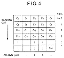
- A code error correcting circuit (ECT) for interleaving original data comprising a sequence of bit data having a length of p bits (p: natural number) by arranging the bit data of the original data into a hypothetical matrix of I (I: natural number not less than 2) rows and J (J: natural number not less than 2) columns and then selecting the bit data positioned on the ith (i: natural number, 1 ≦ i ≦ I ) row along an order of the jth (j: natural number, 1 ≦ j ≦ J ) column, characterized in that said code error correcting circuit comprises:a memory unit (2) having a plurality of memory areas each having a length of 2n bits (n: natural number);a controller (1) for storing the original data to be interleaved into the memory areas respectively;a first data generating device (6, 7, 8) for generating a first data indicating a position of the ith row in the hypothetical matrix;a second data generating device (9, 10, 11) for generating a second data indicating a position of the jth column in the hypothetical matrix;an address decoding device (14) for generating address data indicating one of the memory areas, in which the bit data positioned on the jth column are stored, on the basis of the first data and the second data; anda select data decoding device (15) for generating a bit select data indicating the bit data positioned on the ith row among the bit data stored in said one of the memory areas, which is indicated by the address data, on the basis of the first data and, the second data,said controller controlling said, first data generating device, said second data generating device, said address decoding device and said select data decoding device so that the bit data, which are indicated by the bit select data, stored in said memory unit are sequentially outputted along an order of the ith row and the jth column in the hypothetical matrix as the interleaved original data.
- A code error correcting circuit (ECT) according to claim 1, characterized in that said code error correcting circuit further comprises:a data holding device (16) for holding the sequence of the bit data having a length of 2n bits, which are read out from the memory area corresponding to the address data; anda bit selecting device (17) for selecting the bit data indicated by the bit select data from among the sequence of the bit data having the length of 2n bits held by said data holding device, and outputting the selected bit data as the interleaved data.
- A code error correcting method of interleaving original data comprising a sequence of bit data having a length of p bits (p: natural number) by arranging the bit data of the original data into a hypothetical matrix of I (I: natural number not less than 2) rows and J (J: natural number not less than 2) columns and then selecting the bit data positioned on the ith (i: natural number, 1 ≦ i ≦ I ) row along an order of the jth (j: natural number, 1 ≦ j ≦ J ) column, characterized in that said code error correcting method comprises:a controlling process of storing the original data to be interleaved into a plurality of memory areas each having a length of 2n bits (n: natural number) of a memory unit (2) respectively;a first data generating process of generating a first data indicating a position of the ith row in the hypothetical matrix;a second data generating process of generating a second data indicating a position of the jth column in the hypothetical matrix;an address decoding process of generating address data indicating one of the memory areas, in which the bit data positioned on the jth column are stored, on the basis of the first data and the second data;a select data decoding process of generating a bit select data indicating the bit data positioned on the ith row among the bit data stored in said one of the memory areas, which is indicated by the address data, on the basis of the first data and the second data; andan outputting process of outputting the bit data, which are indicated by the bit select data, stored in said memory unit sequentially along an order of the ith row and the jth column in the hypothetical matrix as the interleaved original data.
- A code error correcting method according to claim 3, characterized in that said code error correcting method further comprises:a data holding process of holding the sequence of the bit data having a length of 2n bits, which are read out from the memory area corresponding to the address data; anda bit selecting process of selecting the bit data indicated by the bit select data from among the sequence of the bit data having the length of 2n bits held by said data holding process, and outputting the selected bit data as the interleaved data.
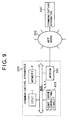
- A communicating apparatus (200) comprising(i) a code error correcting circuit (ECT) for interleaving original data comprising a sequence of bit data having a length of p bits (p: natural number) by arranging the bit data of the original data into a hypothetical matrix of I (I: natural number not less than 2) rows and J (J: natural number not less than 2) columns and then selecting the bit data positioned on the ith (i: natural number, 1 ≦ i ≦ I ) row along an order of the jth (j: natural number, 1 ≦ j ≦ J ) column, and(ii) a transmitting device (201) for transmitting the interleaved original data,
characterized in that said code error correcting circuit comprises:a memory unit (2) having a plurality of memory areas each having a length of 2n bits (n: natural number);a controller (1) for storing the original data to be interleaved into the memory areas respectively;a first data generating device (6, 7, 8) for generating a first data indicating a position of the ith row in the hypothetical matrix;a second data generating device (9, 10, 11) for generating a second data indicating a position of the jth column in the hypothetical matrix;an address decoding device (14) for generating address data indicating one of the memory areas, in which the bit data positioned on the jth column are stored, on the basis of the first data and the second data; anda select data decoding device (15) for generating a bit select data indicating the bit data positioned on the ith row among the bit data stored in said one of the memory areas, which is indicated by the address data, on the basis of the first data and the second data,said controller controlling said first data generating device, said second data generating device, said address decoding device and said select data decoding device so that the bit data, which are indicated by the bit select data, stored in said memory unit are sequentially outputted along an order of the ith row and the jth column in the hypothetical matrix as the interleaved original data. - A communicating method comprising(i) a code error correcting method of interleaving original data comprising a sequence of bit data having a length of p bits (p: natural number) by arranging the bit data of the original data into a hypothetical matrix of I (I: natural number not less than 2) rows and J (J: natural number not less than 2) columns and then selecting the bit data positioned on the ith (i: natural number, 1 ≦ i ≦ I ) row along an order of the jth (j: natural number, 1 ≦ j ≦ J ) column, and(ii) a transmitting process of transmitting the interleaved original data,
characterized in that said code error correcting method comprises:a controlling process of storing the original data to be interleaved into a plurality of memory areas each having a length of 2n bits (n: natural number) of a memory unit (2) respectively;a first data generating process of generating a first data indicating a position of the ith row in the hypothetical matrix;a second data generating process of generating a second data indicating a position of the jth column in the hypothetical matrix;an address decoding process of generating address data indicating one of the memory areas, in which the bit data positioned on the jth column are stored, on the basis of the first data and the second data;a select data decoding process of generating a bit select data indicating the bit data positioned on the ith row among the bit data stored in said one of the memory areas, which is indicated by the address data, on the basis of the first data and the second data; andan outputting process of outputting the bit data, which are indicated by the bit select data, stored in said memory unit sequentially along an order of the ith row and the jth column in the hypothetical matrix as the interleaved original data.
Applications Claiming Priority (2)
| Application Number | Priority Date | Filing Date | Title |
|---|---|---|---|
| JP25696099A JP3973066B2 (en) | 1999-09-10 | 1999-09-10 | Code error correction circuit and code error correction method |
| JP25696099 | 1999-09-10 |
Publications (2)
| Publication Number | Publication Date |
|---|---|
| EP1083663A2 true EP1083663A2 (en) | 2001-03-14 |
| EP1083663A3 EP1083663A3 (en) | 2004-06-23 |
Family
ID=17299772
Family Applications (1)
| Application Number | Title | Priority Date | Filing Date |
|---|---|---|---|
| EP00119368A Withdrawn EP1083663A3 (en) | 1999-09-10 | 2000-09-08 | Code error correcting circuit, code error correcting method, communicating apparatus and communicating method |
Country Status (3)
| Country | Link |
|---|---|
| US (1) | US6701468B1 (en) |
| EP (1) | EP1083663A3 (en) |
| JP (1) | JP3973066B2 (en) |
Families Citing this family (5)
| Publication number | Priority date | Publication date | Assignee | Title |
|---|---|---|---|---|
| JP2003168287A (en) | 2001-07-24 | 2003-06-13 | Toshiba Corp | Memory module, memory system, and data transfer method |
| KR100518295B1 (en) * | 2003-03-14 | 2005-10-04 | 삼성전자주식회사 | Digital communication system having a deinterleaver and a method deinterleaving thereof |
| US9001921B1 (en) * | 2004-02-18 | 2015-04-07 | Marvell International Ltd. | Circuits, architectures, methods, algorithms, software, and systems for improving the reliability of data communications having time-dependent fluctuations |
| CN101159510B (en) * | 2007-11-16 | 2011-09-28 | 海能达通信股份有限公司 | Method for improving dependability of information bit transmission |
| US8661320B2 (en) * | 2011-10-07 | 2014-02-25 | Aeroflex Colorado Springs Inc. | Independent orthogonal error correction and detection |
Family Cites Families (16)
| Publication number | Priority date | Publication date | Assignee | Title |
|---|---|---|---|---|
| JPH07105638A (en) * | 1993-10-05 | 1995-04-21 | Matsushita Electric Ind Co Ltd | Image data recording / reproducing device |
| US5636224A (en) * | 1995-04-28 | 1997-06-03 | Motorola Inc. | Method and apparatus for interleave/de-interleave addressing in data communication circuits |
| US5898710A (en) * | 1995-06-06 | 1999-04-27 | Globespan Technologies, Inc. | Implied interleaving, a family of systematic interleavers and deinterleavers |
| US5818789A (en) * | 1995-10-10 | 1998-10-06 | Holtek Microelectronics, Inc. | Device and method for memory access |
| US5828671A (en) * | 1996-04-10 | 1998-10-27 | Motorola, Inc. | Method and apparatus for deinterleaving an interleaved data stream |
| JPH09288895A (en) * | 1996-04-19 | 1997-11-04 | Toshiba Corp | Ternary storage semiconductor storage system |
| JP2865078B2 (en) * | 1996-10-02 | 1999-03-08 | 日本電気株式会社 | Semiconductor storage device |
| US5912898A (en) * | 1997-02-27 | 1999-06-15 | Integrated Device Technology, Inc. | Convolutional interleaver/de-interleaver |
| TW378330B (en) * | 1997-06-03 | 2000-01-01 | Fujitsu Ltd | Semiconductor memory device |
| US5928371A (en) * | 1997-07-25 | 1999-07-27 | Motorola, Inc. | Systems for programmably interleaving and de-interleaving data and method thereof |
| US6014761A (en) * | 1997-10-06 | 2000-01-11 | Motorola, Inc. | Convolutional interleaving/de-interleaving method using pointer incrementing across predetermined distances and apparatus for data transmission |
| JP4002327B2 (en) * | 1997-11-04 | 2007-10-31 | 株式会社日立製作所 | Digital signal processing circuit |
| US6178530B1 (en) * | 1998-04-24 | 2001-01-23 | Lucent Technologies Inc. | Addressing scheme for convolutional interleaver/de-interleaver |
| KR100323254B1 (en) * | 1998-04-24 | 2002-02-04 | 아끼구사 나오유끼 | Semiconductor integrated circuit |
| JP3629144B2 (en) * | 1998-06-01 | 2005-03-16 | 株式会社東芝 | Nonvolatile semiconductor memory device |
| US6353900B1 (en) * | 1998-09-22 | 2002-03-05 | Qualcomm Incorporated | Coding system having state machine based interleaver |
-
1999
- 1999-09-10 JP JP25696099A patent/JP3973066B2/en not_active Expired - Fee Related
-
2000
- 2000-09-08 US US09/657,805 patent/US6701468B1/en not_active Expired - Fee Related
- 2000-09-08 EP EP00119368A patent/EP1083663A3/en not_active Withdrawn
Also Published As
| Publication number | Publication date |
|---|---|
| JP3973066B2 (en) | 2007-09-05 |
| EP1083663A3 (en) | 2004-06-23 |
| JP2001084155A (en) | 2001-03-30 |
| US6701468B1 (en) | 2004-03-02 |
Similar Documents
| Publication | Publication Date | Title |
|---|---|---|
| US5754566A (en) | Method and apparatus for correcting a multilevel cell memory by using interleaving | |
| US6035427A (en) | Convolutional interleaver and method for generating memory address therefor | |
| CA2277474C (en) | Interleaving method, interleaving apparatus, and recording medium in which interleave pattern generating program is recorded | |
| KR100369273B1 (en) | Semiconductor disk device | |
| US4979175A (en) | State metric memory arrangement for a viterbi decoder | |
| US6253349B1 (en) | Error detective information adding equipment | |
| KR840005869A (en) | Method and apparatus for storing digital data in video format | |
| US6523146B1 (en) | Operation processing apparatus and operation processing method | |
| CN1104682C (en) | Method and apparatus for deinterleaving interleaving data stream | |
| US4570221A (en) | Apparatus for sorting data words on the basis of the values of associated parameters | |
| US6701468B1 (en) | Code error correcting circuit, code error correcting method, communicating apparatus and communicating method | |
| US6127950A (en) | Transmission circuit and reception circuit | |
| JP3550369B2 (en) | Method for storing path metric in Viterbi decoder | |
| EP0608848A2 (en) | Cyclic coding and cyclic redundancy code check processor | |
| JP3784896B2 (en) | Viterbi decoder logic block | |
| US20080244358A1 (en) | Circuits and Methods for Error Coding Data Blocks | |
| US6081213A (en) | Method and apparatus for arithmetic coding, method and apparatus for arithmetic decoding, and storage medium | |
| KR100304193B1 (en) | Inverse circuit of reed-solomon decoder | |
| US5781564A (en) | Method and apparatus for detecting and concealing data errors in stored digital data | |
| US7861146B2 (en) | Viterbi decoding apparatus and Viterbi decoding method | |
| US7526712B2 (en) | Deinterleaving apparatus and method using inner memory and outer memory | |
| JP4563834B2 (en) | Data communication system | |
| JP3288262B2 (en) | Data interleave circuit | |
| US6687870B1 (en) | Method and apparatus for interleaving for information transmission or storage applications | |
| JP2001084155A5 (en) |
Legal Events
| Date | Code | Title | Description |
|---|---|---|---|
| PUAI | Public reference made under article 153(3) epc to a published international application that has entered the european phase |
Free format text: ORIGINAL CODE: 0009012 |
|
| AK | Designated contracting states |
Kind code of ref document: A2 Designated state(s): AT BE CH CY DE DK ES FI FR GB GR IE IT LI LU MC NL PT SE |
|
| AX | Request for extension of the european patent |
Free format text: AL;LT;LV;MK;RO;SI |
|
| PUAL | Search report despatched |
Free format text: ORIGINAL CODE: 0009013 |
|
| AK | Designated contracting states |
Kind code of ref document: A3 Designated state(s): AT BE CH CY DE DK ES FI FR GB GR IE IT LI LU MC NL PT SE |
|
| AX | Request for extension of the european patent |
Extension state: AL LT LV MK RO SI |
|
| 17P | Request for examination filed |
Effective date: 20040928 |
|
| AKX | Designation fees paid |
Designated state(s): DE FR GB |
|
| 17Q | First examination report despatched |
Effective date: 20050415 |
|
| STAA | Information on the status of an ep patent application or granted ep patent |
Free format text: STATUS: THE APPLICATION IS DEEMED TO BE WITHDRAWN |
|
| 18D | Application deemed to be withdrawn |
Effective date: 20080401 |