EP1082666B1 - Compression and decompression of serial port data and status using direct memory access - Google Patents
Compression and decompression of serial port data and status using direct memory access Download PDFInfo
- Publication number
- EP1082666B1 EP1082666B1 EP99909759A EP99909759A EP1082666B1 EP 1082666 B1 EP1082666 B1 EP 1082666B1 EP 99909759 A EP99909759 A EP 99909759A EP 99909759 A EP99909759 A EP 99909759A EP 1082666 B1 EP1082666 B1 EP 1082666B1
- Authority
- EP
- European Patent Office
- Prior art keywords
- data
- destination
- dma
- block
- source
- Prior art date
- Legal status (The legal status is an assumption and is not a legal conclusion. Google has not performed a legal analysis and makes no representation as to the accuracy of the status listed.)
- Expired - Lifetime
Links
Images


Classifications
-
- G—PHYSICS
- G06—COMPUTING; CALCULATING OR COUNTING
- G06F—ELECTRIC DIGITAL DATA PROCESSING
- G06F13/00—Interconnection of, or transfer of information or other signals between, memories, input/output devices or central processing units
- G06F13/14—Handling requests for interconnection or transfer
- G06F13/20—Handling requests for interconnection or transfer for access to input/output bus
- G06F13/28—Handling requests for interconnection or transfer for access to input/output bus using burst mode transfer, e.g. direct memory access DMA, cycle steal
Definitions
- the invention relates to microcontrollers, and more specifically, to a microcontroller providing an improved direct memory access controller for use in conjunction with a serial interface.
- a microcontroller or an embedded controller, is uniquely suited to combining functionality onto one monolithic semiconductor substrate (i.e. chip). By embedding various communication features within a single chip, a communications microcontroller may support a wide range of communication applications.
- Microcontrollers have been used for many years in many applications. A number of these applications involve communications over electronic networks, such as telephone lines, computer networks, and local and wide area networks, in both digital and analog formats.
- a microcontroller In communications applications, a microcontroller generally has a number of integrated communications peripherals in addition to the execution unit. These can be low and high speed serial ports, as well as more sophisticated communications peripherals, such as a universal serial bus (USB) interface, and high level data link control (HDLC) channels.
- USB universal serial bus
- HDMI high level data link control
- An asynchronous serial communications port is one such common additional feature in a microcontroller.
- An asynchronous serial link allows the microcontroller to communicate with other devices or over data lines by sequentially sending and receiving bits of data.
- the "asynchronous" nature indicates these ports do not provide a separate clock signal to clock the data. Instead, the rate at which data is sent and received must be predetermined or prenegotiated, and independently controlled on both the sending and receiving ends.
- This data rate is known as the baud rate, which is the inverse of one bit period.
- the baud rate is generally one of a number of predefined rates, which are standard within the industry. Such rates include 1200, 2400, 4800, 9600, 19.2K, 28.8K, 33.3K, and 54K baud and high data transfer rates.
- microcontrollers include one or more asynchronous serial ports (ASPs) which can transmit and receive data one bit at a time. Such microcontrollers typically employ interrupt signals to notify the microprocessor core that an ASP requires services.
- An ASP typically issues an interrupt request signal when a data unit has been received by the ASP and needs to be transferred from the ASP to an external memory unit, when the ASP is finished transmitting a data unit and the next data unit to be transmitted must be transferred from the external memory unit to the ASP, or when an error occurs.
- An ASP can be configured for a variety data formats, although historically seven or eight data bits are typical values.
- a number of nine-bit serial protocols have been developed using microcontrollers, including a nine-bit asynchronous serial protocol in conjunction with direct memory access (DMA). These protocols are described, for example, in the Am186ES Users Manual and Am186ED Users Manual, both by Advanced Micro Devices, Inc. of Sunnyvale, California. As described in these publications, and as discussed below, a separate control bit is set or reset to act as the ninth data bit during transmission and reception of data. To support DMA using such 9-bit protocols, when that particular bit is received as a certain value, an interrupt is caused to indicate that the ninth data bit has in fact been set.
- US-A-5,737,638 discloses a data processing system in which an on-board DMA controller manages DMA transfers between host memory and an adapter memory, and in which data can be compressed or decompressed during the data transfer.
- a direct memory access (DMA) system characterized by: a direct memory access (DMA) controller that includes a source address register, a destination address register, a source increment field, and a destination increment field, wherein, the source increment field and the destination increment field independently control the incrementing of the source address register and the destination address register, and wherein the incrementing of the source address register and the destination address register are further independent of transfer size such that the spacing of data at a source block associated with the source address register or a destination block associated with the destination address register is compressed or expanded during DMA transfers.
- DMA direct memory access
- the DMA controller has source and destination increment values that can be adjusted and are independent of the transfer item size.
- a source pointer and a destination pointer can be set to the source and destination blocks, with the source block containing word sized data whose top byte is to be discarded.
- the source can be set to increment by two after each transfer, and the destination by one. Then, DMA is performed transferring a byte of data from each word in the source, incrementing to the next word, and incrementing to the next byte for the destination. In this way, one byte of data is stripped from each word using DMA with little processor intervention.
- Sequences of data can be read from the serial port, with each 7 or 8 bit value having a corresponding status byte stored by the DMA controller. Once these status bytes are examined for address bits or error bits, the DMA can be programmed to "strip" the unneeded byte of data.
- byte level data can be expanded into words, with extended write bytes appended to the front of data for transfer by the DMA controller to the asynchronous serial ports supporting extended writes.
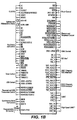
- FIG. 1A shown is a block diagram of a typical microcontroller M implemented according to the invention.
- a microcontroller is preferably implemented on a single monolithic integrated circuit.
- the microcontroller M preferably includes an internal bus 100 coupling, an execution unit 124, system peripherals 174, memory peripherals 176 and serial communication peripherals 172.
- the execution unit 124 in the disclosed embodiment is compatible with the AM186 instruction set implemented in a variety of microcontrollers from Advanced Micro Devices, Inc., of Sunnyvale, California. A variety of other execution units could be used instead of the execution unit 124.
- the system peripherals 174 include a watch dog timer (WDT) 104 for generating non-maskable interrupts (NMIs), microcontroller resets, and system resets.
- An interrupt controller 108 for supporting thirty-six maskable interrupt sources through the use of fifteen channels is also provided as a system peripheral.
- One disclosed system peripheral is a three channel timer control unit 112.
- the timer control unit 112 includes three 16-bit programmable timers.
- Another system peripheral is a general purpose direct memory access (DMA) unit 116 with four channels 0-3.
- DMA direct memory access
- a programmable I/O unit 132 of the microcontroller M supports user programmable input/output signal (PIOs). In the disclosed embodiment, forty-eight PIOs are provided.
- the memory peripherals 176 of the disclosed microcontroller include a DRAM controller 170, a glueless interface 168 to a RAM or ROM, and a chip select unit 126.
- the DRAM controller 170 is fully integrated into the microcontroller M.
- the chip select unit 126 provides six chip select outputs for use with memory devices and eight chip select outputs for use with peripherals.
- a low speed serial port implemented as a universal asynchronous receiver/transmitter (UART) 136 is provided as a serial communication peripheral.
- the low speed UART 136 is typically compatible with a standard 16550 UART known to the industry.
- Another serial communication peripheral in the disclosed embodiment is a synchronous serial interface (SSI) 140.
- SSI synchronous serial interface
- the microcontroller M acts as a master in the synchronous serial interface 140, which is a standard synchronous serial channel.
- the microcontroller M in the disclosed embodiment is particularly well suited to communications environments.
- the serial communication peripherals 172 of the microcontroller M include a number of high speed communication controllers, including a High-level Data Link Control (HDLC) controller 144, a Universal Serial Bus (USB) controller 146, and a high speed serial port (HSUART) 148.
- the disclosed HDLC controller 144 provides four HDLC channels 164.
- the HDLC channels 164 and the USB controller 146 can be written to and read from by a "SmartDMA" unit 150, a unit which provides for chained buffers that are accessed via pairs of DMA channels.
- the SmartDMA unit 150 allows for a high degree of packetized transfer without excessive execution unit 124 intervention.
- the SmartDMA unit 150 preferably consists of four SmartDMA controllers, SmartDMA0-3, that each consists of a pair of DMA channels.
- the HSUART 148 serves to form an asynchronous serial link across a bus to devices external to the micro-controller M.
- the asynchronous nature indicates that the HSUART 148 does not provide a separate clock signal to clock the data. Instead the rate at which data is sent and received must be predetermined or determined through autobauding and independently controlled on sending and receiving ends. This data rate is known as the baud rate. It should be understood that the microcontroller M may include multiple HSUARTs 148.
- the disclosed HDLC controller 144 also includes an interface multiplexer 162.
- This multiplexer 162 couples the four HDLC channels 164, four time slot assignors (TSA) 166, and a number of external buses.
- TSA time slot assignors
- the HDLC channels 164 can be selectively coupled to a pulse code modulation (PCM) highway, a general circuit interface (GCI), an ISDN oriented modular interface revision 2 (IOM-2) serial bus, a data carrier equipment (DCE) serial interface, and other general and specific interfaces that often use packetized communication.
- PCM pulse code modulation
- GCI general circuit interface
- IOM-2 ISDN oriented modular interface revision 2
- DCE data carrier equipment
- the HDLC channels 164 support HDLC, SDLC, Link Access Procedures Balanced (LAPB), Link Access Procedures on the D-channel (LAPD), and PPP, and as noted above, each include an intependent time slot assignor 166 for assigning a portion of a serial frame to each HDLC for isochronous or isochronous-type communication.
- LAPB Link Access Procedures Balanced
- LAPD Link Access Procedures on the D-channel
- PPP and as noted above, each include an intependent time slot assignor 166 for assigning a portion of a serial frame to each HDLC for isochronous or isochronous-type communication.
- FIG. 1B shown are illustrative pinouts for the microcontroller M implemented according to the invention. Illustrated are clock pinouts for the clock 102, address and address/data bus pinouts to the bus interface unit 120, bus status and control pinouts, again generally for the bus interface unit 120, timer control pinouts coupled to the timer control unit 112, USB control and transceiver control pinouts for the USB controller 146, synchronous serial controller pinouts for the synchronous serial interface 140, programmable I/O pinouts for the programmable I/O unit 132, reset control pinouts, memory and peripheral control pinouts coupled to both the chip select unit 126 and the bus interface unit 120, DMA control pinouts for the general purpose DMA unit 116 and the SmartDMA unit 150, HDLC channel/DCE interface/PCM interface pinouts for coupling to the HDLC controller 144, UART pinouts for the low speed UART 136, and high speed UART pinouts for the HSUART 148.
- pinouts are illustrative, and a wide variety of other functional units and associated pinouts could be used without detracting from the spirit of the invention.
- a number of both the communications and general purpose peripherals from Figure IA could be eliminated, or added to, without detracting from the spirit of the invention.
- microcontroller itself has differing definitions in industry. Some companies refer to a processor core with additional features (such as I/O) as a “microprocessor” if it has no onboard memory, and digital signal processors (DSPs) are now used for both special and general purpose controller functions. As here used, the term “microcontroller” covers all of the products, and generally means an execution unit with added functionality all implemented on a single monolithic integrated circuit
- DMA unit 116 and the high speed UART 148, here described as an asynchronous serial port (ASP) 148.
- ASP asynchronous serial port
- the ASP 148 can support an asynchronous serial protocol that employs an "address bit" as an extra serial bit.
- the ASP 148 transmits or receives 7 or 8 data bits 202. These are standard data bits sent in an asynchronous protocol, low order bit first. After the 7 or 8 data bits 202, however, the address bit protocol supported by the ASP 148 provides for an optional address bit AB 204. This address bit is typically either the 8th or 9th bit transmitted or received by the ASP 148, and is typically used in applications such as multi-drop applications that require one master device to control multiple slave devices. Although called an address bit, this bit can act as an extended bit that effectively causes interrupts within the slave devices for flow and other control. This address bit protocol is known to the art
- an optional parity bit PB 206 is then followed by a stop bit ST 208, and then an optional second stop bit ST 210.
- the DMA unit 116 and the ASP 148 have additional features according to the invention that may be useful in sending and receiving data that employs an address bit AB 204 as illustrated in Figure 3. These features are best understood by examining a set of registers within the DMA unit 116 and the ASP 148, here shown as DMA registers 212 and ASP registers 214.
- the DMA registers 212 will be further discussed in conjunction with Figures 6A-6E, and the ASP registers 214 will be further discussed in conjunction with Figures 7A-7G.
- the DMA unit 116 can compress and decompress data during transfers between a source and a destination that have two differing data sizes. For example, the DMA unit 116 can read data byte-by-byte from a source memory block, and write each read byte of data as the low (or high) order byte of consecutive words in a destination memory block. Conversely, the DMA unit can read the low order byte of consecutive words of data from a source block, and then store those read bytes consecutively in a destination block. This is especially helpful in conjunction with the ASP 148 when it is used in an extended read and write mode.
- the ASP 148 can read in 7 or 8 bit data units over a serial line, but store that data into a 16-bit word along with both an address bit and status bits corresponding to that I/O read.
- Figure 7G discussed below, but to summarize, parity errors, overrun errors, framing errors, character matches, breaks, the address bit, and other status can be stored along with 7 or 8 bits of data actually received.
- this allows the execution unit 124 to go back and examine the received data to determine where any errors may have occurred or address bits may have been set, and process the data accordingly.
- the execution unit 124 can then simply store the data as 7 or 8 bit data within bytes instead of as words.
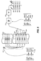
- the DMA unit 116 is especially advantageous. Referring to Figure 4, illustrated is the DMA unit 116 processing data from the ASP unit 148 as discussed.
- the DMA unit 116 stores this data in a memory 216 as a series of data and status bytes within a block 218, shown as DATA1, STATUS1, DATA2, STATUS2, etc. So, each 7 or 8 bit data value DATA1-DATAn occupies 16 bits when combined with its associated status byte STATUS1-STATUSn.
- the DMA unit 116 can then be programmed by the execution unit 124 to perform a transfer from the block 218 to another block 220 in the memory 216, but this block to include simply a number of the consecutive data values DATA1-DATAn but without the associated status.
- the DMA unit 116 first reads the first data item DATA1 and from the block 218 then writes it to the destination location DATA1 in the block 220. Then, however, the DMA unit 116 increments the destination address within the block 220 by 1 but simultaneously increments the source address in the block 218 by 2. Therefore, the next data item read from the block 218 is DATA2 (STATUS1 is skipped), which is then written as a byte in the destination block 220 immediately after the first data item DATA1. This is repeated, compressing the data such that the original 16-bit data and status values are now simply 8-bit data values.
- a source data block 222 contains data that the microcontroller M should transmit to an external asynchronous serial line.
- This data includes four data items DATA4 that each occupy 7 or 8 bits within a byte of memory.
- the DMA unit 116 is programmed to read the first of these data items DATA1 in the block 222, and then write that data item DATA1 into a destination block 224. Then, the source address within the data block 222 is incremented, but the destination address within the destination block 224 is incremented by 2. Thus, the next data item DATA2 is read from the source block 222, but is written 2 bytes later into the destination block 224.
- the execution unit 124 Before that data is actually transmitted, it may be desirable for the execution unit 124 to clear address bits that are stored in the intervening bytes of the data items DATA1-DATA4 in the destination block 224. Here, three address bits 226 are shown cleared, and one address bit 228 set.
- the DMA unit 116 is then programmed to perform word-size writes to the ASP 148 using the extended write capability of the ASP 148.
- the low order bit of the high order byte is then used as the address bit for transmission of data, resulting in four illustrated data items 230, 232, 234, and 236, the first of which has its address bit set and the remainder of which do not.
- the DMA unit 116 may include more than one DMA channel, and those DMA channels can be implemented as circular buffers. It would be further possible to implement two channels in Figure 4 such that one channel was reading extended data from the ASP 148 and then writing it into a circular buffer implemented as the buffer 218, and then a second channel was reading from the buffer 218, compressing the data into the destination buffer 220.
- the execution unit 124 is relieved of the processing overhead required to strip or add unneeded status information from or to data before the DMA unit 116 sends or receives data to the ASP 148.
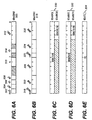
- FIGS 6A-6E illustrated are five of the DMA registers 212 employed to implement the compression and decompression according to the invention.
- FIG 6A illustrated is a general purpose DMA channel "x" control register GDxCON0 300. (Note with four channels, the "x" would be from 1 to 4.)
- the GDxCON0 register 300 includes a number of standard general purpose DMA control bits, such as a start/stop bit ST 302, an auto start bit AST 304, a terminal count stop bit TC 306, an interrupt enable bit INT 308, a priority field P 310, and a DMA request source field DSEL 312.
- the GDxCON1 register 316 also includes a number of standard DMA bits, such as a source address space select bit SM/*IO 318, a source address wrap field SAW 320, a destination address space select bit DM/*IO 322, and a destination address wrap field DAW 324.
- the SM/*IO bit 318 and the DM/*IO bit 322 select whether the source and destination space will be memory or I/O.
- a source increment field SINC 326 and a destination increment field DINC 328 are 4-bit 2's complements values that are added to the source and destination pointer after each transfer. For example, if the SINC field 326 or the DINC field 328 are 0, there is no increment If they are equal to a binary 1, or 4'b0001, the fields are incremented by 1. If they equal 4'b0010, the pointers are incremented by 2 bytes, if equal to 4'b0011, incremented by 3 bytes, and so on. For negative values the opposite is true. For example, using 2's complement format, if the SINC or DINC fields 326 or 328 are equal to 4'b1111, the source or destination address will be decremented by 1 after the transfer.
- FIG. 6C and 6D illustrated are source address registers 330 and destination address registers 332.
- FIG. 6E illustrated is a transfer count register 334.
- the DMA unit 116 for the transfer between the ASP 148 and the destination block 218, the DMA unit 116 is programmed with a set of values 336. Specifically, the source is set to be from an I/O location, and to increment by 0 after each transfer (appropriate for an I/O location), and the destination is set to memory and is set to increment by 2 after each transfer. Further, the data size is set to a word. This provides that each transfer will be a 16-bit extended serial read value from the ASP 148, which is stored word-by-word in the destination block 218.
- the DMA unit 116 is programmed with a set of values 338. Specifically, the source is set in memory (and the source address 330 will be set to the start of the source block 218), and is set to increment by 2 after each transfer. The destination is also set in memory, but the destination address is incremented by only 1 after each transfer. Finally, the transfer size is set for I byte. This means that 1 byte will be read from the source block 218 and written to the destination block 220 as DATA1. The source address 330, however, will then be incremented by 2, while the destination address 332 will only be incremented by 1. Then a second byte of data, DATA2, will be read from the source block 218 and written immediately after DATA1 in the destination block 220. Thus, unneeded status information in STATUS1 is skipped.
- the destination block 220 could be programmed to actually overlap with the source block 218 because after the data is read from the source block 218, it is no longer needed.
- the source buffer can literally be used as the destination buffer, saving memory space.
- the expansion capability of the DMA unit 116 is illustrated by a set of programmed values 340.
- the source block 222 of 8-bit data is expanded by setting the DMA unit 116 to transfer from memory to memory, by setting the SINC field 326 to a value of 1, but setting the DINC field 328 to a value of 2.
- the transfer size bit TS 314 is set to 0, such that data is transferred a byte at a time.
- a data byte is read from the source block 222 and written to the destination block 224, but the next data byte consecutively read from the source block 222 is written 2 bytes later in the destination block 224.
- the execution unit 124 can then appropriately set or reset the address bits AB, in the destination block 224, and institute a second DMA transfer to the ASP 148.
- a set of programmed values 342 is used, which provide for a source in memory and destination in I/O space, and provide for a source increment SINC 326 value of 2 and no destination increment.
- the transfer size bit TS 314 is set to 1 for word transfers. This results in the extended data being written to the ASP 148, so that it can control the 9th, address bit on its transmission of serial data.
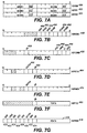
- Figure 7A illustrated are certain of the ASP registers 214 that implement another feature according to the invention.
- Figure 7A illustrates 6 character match bytes employed by the ASP 148 for matching characters of received data.
- three registers HSPM0 400, HSPM1 402, and HSPM2 404 contain 6 character match values MCHR0 406 through MCHR5 415.
- FIG. 7G illustrates an asynchronous serial port 418 receive register HSPRXD 416.
- This register contains a 7 or 8 bit value received data RDATA 418, but also contains 8 status bits 420 through 434.
- additional bits are provided such that when set, the address bit value AB 434 is matched in addition to the RDATA value RDATA 418.
- HP CONO 436 This is better understood in conjunction with a high speed serial port control register HP CONO 436, illustrated in Figure 7C.
- This register in part provides configuration settings to determine whether an address bit is going to be employed (indicated by an ABEN bit 442), whether the parity bits PB 206 will be used (indicated by a parity enable bit PEN 440), whether 7 or 8 bit data will be used and thus whether the D7 bit of the bits 202 will be used (indicated by enable bit D7 444), and whether the second stop bit ST2 210 will be used (indicated by a second stop bit enable bit STP2 446).
- an address bit set or reset bit AB 438 sets or resets the transmitted address bit, as long address bit communication is enabled (controlled by the ABEN bit 442).
- All of these bits 438 through 446 affect the length of a transmitted frame.
- the receive data 418 is 7-bit data (the D7 bit 444 false) and an address bit is enabled (the ABEN bit 442 is true)
- the RDATA 418 would not include the address bit. Instead, that would still be stored in the high order byte of the HSPRXD register 416 as the address bit AB 434. Thus, that bit would never be matched with any of the match characters MCHR0 406 through MCHR5 415.
- additional match character address bit MATCH bits are provided in a second control register HSPCON1 448.
- this register 448 includes a match enable bit MEN 450, which when true, enables the character matching of the MCHR0 406 through MCHR5 415.
- additional character matching bits are provided.
- Three match address bits MAB2 452, MAB1 454, and MAB0 456 effectively become an address bit matching bit for the three match registers HSPMO 400 through HSPM2 404 when the address bit is enabled by the ABEN bit 442 of the control register HSPCON0 436.
- a received character must have its address bit AB 204 clear to match characters in the HSPM2 register 404.
- the MAB2 bit 452 is set, and the ABEN bit 442 is true, a received character must have its address bit AB 204 set in order to match characters in the HSPM2 register 404.
- the MAB1 bit 454 and the MAB0 bit 456 similarly correspond to the HSPM1 register 402 and the HSPM0 register 400.
- these additional bits in the HSPCON1 register 448 provide for address matching for corresponding ones of the HSPM0 register 400 through HSPM2 register 404.
- the ASP 148 could be set up where one of the registers HSPM0 400 through HSPM2 404 was set for character matching, while the other two were set for address matching.
- the HSPCON1 register 448 further includes an extended write bit 458 and an extended read bit 460, which provide, when true, that 16-bit data will be read from a transmit register HSPTXD 462 (see Fig. 7F) or received in the receive register HSPRXD 416 (see Fig. 7G). When these values are disabled, only 8-bit data is stored in those registers, and the address bit and the match status can only be determined by reading a status register HPSTAT 464 (see Fig. 7D).
- That status register 464 includes a match bit MATCH 466 which is set true if the incoming data is a character or address match (as appropriate) to one of the HSPM0-HSPM2 registers 400-402 and an address bit AB 468 which is set true if the incoming data has its address bit set.
- An interrupt mask register HSPIMSK 470 correspondingly passes on the match bit MATCH 466 and the address AB 468 as interrupts.
- a host system 500 transmits serial data to multiple multidrop peripherals 502, 504, and 506.
- Each of these peripherals includes a microcontroller M of its own 508, 510, and 512.
- Each of these can be programmed such that it had a unique address 1, 2, and 3 for the peripherals 502, 504, and 506.
- Each can be placed into an idle mode where received characters are effectively dumped by each of the peripherals 502, 504, and 506 until one of the peripherals has an address match.
- the microcontroller 508 of the peripheral 502 could be programmed such that the MCHR0 byte 406 contained the appropriate addressing information, including the "1" address assigned to the peripheral 502, and its associated address matching bit MAB0 456 would be set, along with the address bit enable ABEN 442. In this way, when the host 500 sent a frame of asynchronous data with the appropriate address matching MCHRO 406 to the peripheral 502, that data would match the character in MCHR0 406 and the address bit being set would match the MAB0 456 bit.
- the match bit MATCH 466 would be set in the HPSTAT register 464, and, assuming the match interrupt was set to pass in the HSPIMSK register 470, an interrupt would be passed to the execution unit 124 so that the peripheral 502 could be awaken and set to process subsequent data.
- the asynchronous serial port could not only detect the start and end of data frames based on matchable character data, but can also detect when a particular microcontroller is being addressed in a multidrop system by also matching the address bit This provides for added flexibility in applications of the microcontroller M.
Description
Claims (8)
- A direct memory access (DMA) system, characterized by:a direct memory access (DMA) controller (116) that includes a source address register (330), a destination address register (332), a source increment field (326), and a destination increment field (328),wherein, the source increment field (326) and the destination increment field (328) independently control the incrementing of the source address register (330) and the destination address register (332), andwherein the incrementing of the source address register (330) and the destination address register ( 332) are further independent of transfer size such that the spacing of data at a source block (218, 222) associated with the source address register (330) or a destination block (220, 224) associated with the destination address register (332) is compressed or expanded during DMA transfers.
- A DMA system as claimed in claim 1 wherein the incrementing of the source address register and the destination address register is independently controlled such that a portion of the data located in a block pointed by the destination address is skipped during transfer from the source address to the destination address.
- A DMA system as claimed in claim 1, wherein the DMA controller (116) is configurable such that in performing a DMA transfer non-consecutive data at a source block (218, 222) associated with the source address register (330) becomes consecutive data at a destination block (220, 224) associated with the destination address register (332).
- A DMA system as claimed in claim 1, wherein the DMA controller (116) is configurable such that in performing a DMA transfer consecutive data at a source block (218, 222) associated with the source address register (330) becomes non-consecutive data at a destination block (220, 224) associated with the destination address register (332).
- A method of compressing or expanding spacing of data within a memory employing a DMA controller (116) comprising the steps of:setting the DMA controller (116) to point to a source block (218, 222) and to destination block (220, 224);setting the DMA controller (116) to increment a source address pointing to the source block (218, 222) by a first predetermined amount of data;setting the DMA controller (116) to increment a destination address pointing to the destination block (220, 224) by a second predetermined amount of data not equal to the first predetermined amount of data; andperforming a DMA transfer such that spacing of data at the source block (218, 222) or the destination block (220, 224) is compressed or expanded.
- A method as claimed in claim 5, wherein by performing the DMA transfer non-consecutive data in the source block (218, 222) becomes consecutive data in the destination block (220, 224).
- A method as claimed in claim 5, wherein by performing the DMA transfer consecutive data in the source block (218, 222) becomes non-consecutive data in the destination block (220, 224).
- A method as claimed in claim 5, wherein the source block (218, 222) contains data information and associated status information and in performing the DMA transfer only the data information is written to the destination block (220, 224).
Applications Claiming Priority (3)
| Application Number | Priority Date | Filing Date | Title |
|---|---|---|---|
| US09/088,133 US6385670B1 (en) | 1998-06-01 | 1998-06-01 | Data compression or decompressions during DMA transfer between a source and a destination by independently controlling the incrementing of a source and a destination address registers |
| US88133 | 1998-06-01 | ||
| PCT/US1999/004610 WO1999063447A1 (en) | 1998-06-01 | 1999-03-01 | Compression and decompression of serial port data and status using direct memory access |
Publications (2)
| Publication Number | Publication Date |
|---|---|
| EP1082666A1 EP1082666A1 (en) | 2001-03-14 |
| EP1082666B1 true EP1082666B1 (en) | 2001-11-14 |
Family
ID=22209549
Family Applications (1)
| Application Number | Title | Priority Date | Filing Date |
|---|---|---|---|
| EP99909759A Expired - Lifetime EP1082666B1 (en) | 1998-06-01 | 1999-03-01 | Compression and decompression of serial port data and status using direct memory access |
Country Status (6)
| Country | Link |
|---|---|
| US (1) | US6385670B1 (en) |
| EP (1) | EP1082666B1 (en) |
| JP (1) | JP2002517820A (en) |
| KR (1) | KR100546085B1 (en) |
| DE (1) | DE69900477T2 (en) |
| WO (1) | WO1999063447A1 (en) |
Families Citing this family (4)
| Publication number | Priority date | Publication date | Assignee | Title |
|---|---|---|---|---|
| US6816921B2 (en) * | 2000-09-08 | 2004-11-09 | Texas Instruments Incorporated | Micro-controller direct memory access (DMA) operation with adjustable word size transfers and address alignment/incrementing |
| US7861073B2 (en) * | 2007-01-03 | 2010-12-28 | Apple Inc. | On-chip decompression engine |
| US10275375B2 (en) * | 2013-03-10 | 2019-04-30 | Mellanox Technologies, Ltd. | Network interface controller with compression capabilities |
| US20220374368A1 (en) * | 2021-05-19 | 2022-11-24 | Hughes Network Systems, Llc | System and method for enhancing throughput during data transfer |
Family Cites Families (23)
| Publication number | Priority date | Publication date | Assignee | Title |
|---|---|---|---|---|
| US5208915A (en) * | 1982-11-09 | 1993-05-04 | Siemens Aktiengesellschaft | Apparatus for the microprogram control of information transfer and a method for operating the same |
| US4700391A (en) * | 1983-06-03 | 1987-10-13 | The Variable Speech Control Company ("Vsc") | Method and apparatus for pitch controlled voice signal processing |
| US4642791A (en) * | 1983-09-15 | 1987-02-10 | Pitney Bowes Inc. | Interface for mailing system peripheral devices |
| US4646261A (en) * | 1983-09-27 | 1987-02-24 | Motorola Computer Systems, Inc. | Local video controller with video memory update detection scanner |
| JP2539058B2 (en) * | 1989-03-30 | 1996-10-02 | 三菱電機株式会社 | Data processor |
| JP2527821B2 (en) * | 1989-09-14 | 1996-08-28 | 株式会社日立製作所 | Data processing method and input / output device |
| US4974223A (en) * | 1989-09-18 | 1990-11-27 | International Business Machines Corporation | Parallel architecture for high speed flag detection and packet identification |
| JPH04219859A (en) * | 1990-03-12 | 1992-08-10 | Hewlett Packard Co <Hp> | Harware distributor which distributes series-instruction-stream data to parallel processors |
| DE69128665T2 (en) * | 1990-07-20 | 1998-07-16 | Matsushita Electric Ind Co Ltd | Data mixing device |
| GB2250615B (en) * | 1990-11-21 | 1995-06-14 | Apple Computer | Apparatus for performing direct memory access with stride |
| US5313454A (en) * | 1992-04-01 | 1994-05-17 | Stratacom, Inc. | Congestion control for cell networks |
| JPH06133269A (en) * | 1992-09-02 | 1994-05-13 | Pioneer Electron Corp | Video signal recording and reproducing device |
| FR2716276B1 (en) * | 1994-02-16 | 1996-05-03 | Sgs Thomson Microelectronics | Data reorganization circuit. |
| US5588029A (en) * | 1995-01-20 | 1996-12-24 | Lsi Logic Corporation | MPEG audio synchronization system using subframe skip and repeat |
| US5633865A (en) * | 1995-03-31 | 1997-05-27 | Netvantage | Apparatus for selectively transferring data packets between local area networks |
| US5737638A (en) | 1995-07-14 | 1998-04-07 | International Business Machines Corporation | System for determining plurality of data transformations to be performed upon single set of data during single transfer by examining communication data structure |
| US5761453A (en) * | 1995-12-07 | 1998-06-02 | Apple Computer, Inc. | Method and system for increasing the throughput of serial data in a computer system |
| US5854640A (en) * | 1996-01-02 | 1998-12-29 | Intel Corporation | Method and apparatus for byte alignment of video data in a memory of a host system |
| US5768445A (en) | 1996-09-13 | 1998-06-16 | Silicon Graphics, Inc. | Compression and decompression scheme performed on shared workstation memory by media coprocessor |
| US5982373A (en) * | 1996-11-12 | 1999-11-09 | Chromatic Research, Inc. | Dynamic enhancement/reduction of graphical image data resolution |
| US5896549A (en) * | 1997-02-04 | 1999-04-20 | Advanced Micro Devices, Inc. | System for selecting between internal and external DMA request where ASP generates internal request is determined by at least one bit position within configuration register |
| US5958024A (en) * | 1997-08-29 | 1999-09-28 | Advanced Micro Devices, Inc. | System having a receive data register for storing at least nine data bits of frame and status bits indicating the status of asynchronous serial receiver |
| US5944800A (en) * | 1997-09-12 | 1999-08-31 | Infineon Technologies Corporation | Direct memory access unit having a definable plurality of transfer channels |
-
1998
- 1998-06-01 US US09/088,133 patent/US6385670B1/en not_active Expired - Fee Related
-
1999
- 1999-03-01 JP JP2000552593A patent/JP2002517820A/en active Pending
- 1999-03-01 DE DE69900477T patent/DE69900477T2/en not_active Expired - Lifetime
- 1999-03-01 EP EP99909759A patent/EP1082666B1/en not_active Expired - Lifetime
- 1999-03-01 KR KR1020007013621A patent/KR100546085B1/en not_active IP Right Cessation
- 1999-03-01 WO PCT/US1999/004610 patent/WO1999063447A1/en active IP Right Grant
Also Published As
| Publication number | Publication date |
|---|---|
| KR100546085B1 (en) | 2006-01-26 |
| KR20010052493A (en) | 2001-06-25 |
| EP1082666A1 (en) | 2001-03-14 |
| WO1999063447A1 (en) | 1999-12-09 |
| US6385670B1 (en) | 2002-05-07 |
| JP2002517820A (en) | 2002-06-18 |
| DE69900477T2 (en) | 2002-07-18 |
| DE69900477D1 (en) | 2001-12-20 |
Similar Documents
| Publication | Publication Date | Title |
|---|---|---|
| US6266715B1 (en) | Universal serial bus controller with a direct memory access mode | |
| US5561826A (en) | Configurable architecture for serial communication | |
| US4942515A (en) | Serial communications controller with FIFO register for storing supplemental data and counter for counting number of words within each transferred frame | |
| KR100352224B1 (en) | Direct memory access(dma) transactions on a low pin count bus | |
| USRE41494E1 (en) | Extended cardbus/PC card controller with split-bridge technology | |
| US6609163B1 (en) | Multi-channel serial port with programmable features | |
| US5958024A (en) | System having a receive data register for storing at least nine data bits of frame and status bits indicating the status of asynchronous serial receiver | |
| WO1984001447A1 (en) | Line support processor for data transfer system | |
| WO2002079971A1 (en) | Programmable cpu/interface buffer structure using dual port ram | |
| US20180196764A1 (en) | Computing module with serial data connectivity | |
| EP1076969A1 (en) | Autobauding with adjustment to a programmable baud rate | |
| JPH06209348A (en) | Multiplex station communication bus system | |
| US6332173B2 (en) | UART automatic parity support for frames with address bits | |
| EP0901081B1 (en) | A digital signal processor with peripheral devices and external interfaces | |
| EP1082666B1 (en) | Compression and decompression of serial port data and status using direct memory access | |
| US6105081A (en) | UART character matching used for address matching on a register-by-register basis | |
| US6327259B1 (en) | Flexible placement of serial data within a time divisioned multiplexed frame through programmable time slot start and stop bit positions | |
| JP2001298494A (en) | Controller and method for controlling interface with data link | |
| JP2724322B2 (en) | General-purpose asynchronous receiver-transmitter | |
| US6112262A (en) | System and method for efficiently transferring information between processors | |
| US6311235B1 (en) | UART support for address bit on seven bit frames | |
| US6134609A (en) | Method for using computer system memory as a modem data buffer by transferring modem I/O data directly to system controller and transferring corresponding system controller data directly to main memory | |
| US6442643B1 (en) | System and method for resolving data transfer incompatibilities between PCI and Non-PCI buses | |
| US20030063726A1 (en) | Caller ID data-reporting mechanism for electronic devices and associated methods | |
| KR20070081981A (en) | Interface method and apparatus in cpuless system |
Legal Events
| Date | Code | Title | Description |
|---|---|---|---|
| PUAI | Public reference made under article 153(3) epc to a published international application that has entered the european phase |
Free format text: ORIGINAL CODE: 0009012 |
|
| GRAG | Despatch of communication of intention to grant |
Free format text: ORIGINAL CODE: EPIDOS AGRA |
|
| 17P | Request for examination filed |
Effective date: 20001026 |
|
| AK | Designated contracting states |
Kind code of ref document: A1 Designated state(s): DE FR GB IT |
|
| 17Q | First examination report despatched |
Effective date: 20010307 |
|
| GRAG | Despatch of communication of intention to grant |
Free format text: ORIGINAL CODE: EPIDOS AGRA |
|
| GRAH | Despatch of communication of intention to grant a patent |
Free format text: ORIGINAL CODE: EPIDOS IGRA |
|
| GRAH | Despatch of communication of intention to grant a patent |
Free format text: ORIGINAL CODE: EPIDOS IGRA |
|
| GRAA | (expected) grant |
Free format text: ORIGINAL CODE: 0009210 |
|
| AK | Designated contracting states |
Kind code of ref document: B1 Designated state(s): DE FR GB IT |
|
| PG25 | Lapsed in a contracting state [announced via postgrant information from national office to epo] |
Ref country code: IT Free format text: LAPSE BECAUSE OF FAILURE TO SUBMIT A TRANSLATION OF THE DESCRIPTION OR TO PAY THE FEE WITHIN THE PRESCRIBED TIME-LIMIT;WARNING: LAPSES OF ITALIAN PATENTS WITH EFFECTIVE DATE BEFORE 2007 MAY HAVE OCCURRED AT ANY TIME BEFORE 2007. THE CORRECT EFFECTIVE DATE MAY BE DIFFERENT FROM THE ONE RECORDED. Effective date: 20011114 |
|
| REF | Corresponds to: |
Ref document number: 69900477 Country of ref document: DE Date of ref document: 20011220 |
|
| REG | Reference to a national code |
Ref country code: GB Ref legal event code: IF02 |
|
| ET | Fr: translation filed | ||
| PLBE | No opposition filed within time limit |
Free format text: ORIGINAL CODE: 0009261 |
|
| STAA | Information on the status of an ep patent application or granted ep patent |
Free format text: STATUS: NO OPPOSITION FILED WITHIN TIME LIMIT |
|
| 26N | No opposition filed |
Inventor name: SOBEL, WILLIAM, E. |
|
| REG | Reference to a national code |
Ref country code: GB Ref legal event code: 732E Free format text: REGISTERED BETWEEN 20091210 AND 20091216 |
|
| PGFP | Annual fee paid to national office [announced via postgrant information from national office to epo] |
Ref country code: FR Payment date: 20100318 Year of fee payment: 12 |
|
| PGFP | Annual fee paid to national office [announced via postgrant information from national office to epo] |
Ref country code: GB Payment date: 20100208 Year of fee payment: 12 |
|
| REG | Reference to a national code |
Ref country code: FR Ref legal event code: TP |
|
| PGFP | Annual fee paid to national office [announced via postgrant information from national office to epo] |
Ref country code: DE Payment date: 20110331 Year of fee payment: 13 |
|
| GBPC | Gb: european patent ceased through non-payment of renewal fee |
Effective date: 20110301 |
|
| REG | Reference to a national code |
Ref country code: FR Ref legal event code: ST Effective date: 20111130 |
|
| PG25 | Lapsed in a contracting state [announced via postgrant information from national office to epo] |
Ref country code: FR Free format text: LAPSE BECAUSE OF NON-PAYMENT OF DUE FEES Effective date: 20110331 |
|
| PG25 | Lapsed in a contracting state [announced via postgrant information from national office to epo] |
Ref country code: GB Free format text: LAPSE BECAUSE OF NON-PAYMENT OF DUE FEES Effective date: 20110301 |
|
| REG | Reference to a national code |
Ref country code: DE Ref legal event code: R119 Ref document number: 69900477 Country of ref document: DE Effective date: 20121002 |
|
| PG25 | Lapsed in a contracting state [announced via postgrant information from national office to epo] |
Ref country code: DE Free format text: LAPSE BECAUSE OF NON-PAYMENT OF DUE FEES Effective date: 20121002 |