EP1081861A2 - Gain calibration system and method for creating matched A/D converters - Google Patents
Gain calibration system and method for creating matched A/D converters Download PDFInfo
- Publication number
- EP1081861A2 EP1081861A2 EP20000116959 EP00116959A EP1081861A2 EP 1081861 A2 EP1081861 A2 EP 1081861A2 EP 20000116959 EP20000116959 EP 20000116959 EP 00116959 A EP00116959 A EP 00116959A EP 1081861 A2 EP1081861 A2 EP 1081861A2
- Authority
- EP
- European Patent Office
- Prior art keywords
- converters
- converter
- analog
- outputs
- gain
- Prior art date
- Legal status (The legal status is an assumption and is not a legal conclusion. Google has not performed a legal analysis and makes no representation as to the accuracy of the status listed.)
- Withdrawn
Links
- 238000000034 method Methods 0.000 title abstract description 16
- 238000012937 correction Methods 0.000 claims abstract description 12
- 238000010586 diagram Methods 0.000 description 10
- 230000005355 Hall effect Effects 0.000 description 6
- 238000012986 modification Methods 0.000 description 3
- 230000004048 modification Effects 0.000 description 3
- 238000013459 approach Methods 0.000 description 2
- 238000006243 chemical reaction Methods 0.000 description 2
- 231100001261 hazardous Toxicity 0.000 description 2
- 230000006698 induction Effects 0.000 description 1
- 238000005259 measurement Methods 0.000 description 1
- 229910000679 solder Inorganic materials 0.000 description 1
- 238000004804 winding Methods 0.000 description 1
Images



Classifications
-
- H—ELECTRICITY
- H03—ELECTRONIC CIRCUITRY
- H03M—CODING; DECODING; CODE CONVERSION IN GENERAL
- H03M1/00—Analogue/digital conversion; Digital/analogue conversion
- H03M1/10—Calibration or testing
- H03M1/1009—Calibration
- H03M1/1014—Calibration at one point of the transfer characteristic, i.e. by adjusting a single reference value, e.g. bias or gain error
-
- H—ELECTRICITY
- H03—ELECTRONIC CIRCUITRY
- H03M—CODING; DECODING; CODE CONVERSION IN GENERAL
- H03M1/00—Analogue/digital conversion; Digital/analogue conversion
- H03M1/12—Analogue/digital converters
- H03M1/1205—Multiplexed conversion systems
Definitions
- the present invention relates to analog-to-digital (A/D) converters. More specifically, the present invention relates to systems and methods for matching the outputs of two or more A/D converters.
- A/D analog-to-digital
- the inventive system includes a mechanism for sensing the output of the first converter and a mechanism for sensing the output of the second converter.
- a microprocessor runs software that computes a correction factor in response to the outputs of the first and second converters. The correction factor is used to adjust the output of the second converter to match the gain of the first converter in accordance with the needs of a particular application.
- the correction factor is such that the gain of said second converter is equal to that of the first converter and the software includes code for adjusting the gain of the second converter to be greater than or equal to the output of the first converter.
- the analog inputs to the A/D converters are provided by series sense resistors.
- Fig. 1 is a schematic/block diagram of an illustrative implementation of an application of a system for matching the gains of first and second analog-to-digital converters constructed in accordance with conventional teachings.
- a typical motor drive system 10' current from a three-phase source 12 is rectified to direct current (DC) by a diode rectifier circuit 14.
- the DC current is applied as a level adjusted, simulated, three-phase current to an induction motor 20 via a plurality of drive transistors 16 and 18.
- a controller 30 supplies gate drive voltage to the drive transistors 16 and 18 via isolated gate drive circuits 22 and adjusts the level of same (and thereby the speed of the motor 20) via isolated current sensing circuits 23 and 24.
- the current sensing was effected with Hall effect devices 25 and 26.
- the analog current sensed by the Hall effect devices 25 and 26 was converted to a digital voltage by variable analog to digital converters 27 and 28.
- the digitized voltages were used by the controller to adjust the timing, speed and direction of actuation of the motor 20.
- Fig. 2 is a schematic/block diagram of an illustrative application of a system for matching the gains of first and second analog-to-digital converters constructed in accordance with the teachings of the present invention.
- the system 10 is similar to the system 10' of Fig. 1 with the exception that the inventive system 10 includes isolated modulators 32 and 34 which form first and second A/D converters when combined with digital filters 40 and 42.
- Fig. 3 is block diagram showing the isolated modulator and A/D converter of Fig 2 in greater detail.
- the isolated modulators may be purchased from Hewlett Packard as HCPL 7860.
- the modulators 32 and 34 include a ⁇ modulator 44, an encoder 46 and a light emitting diode 48.
- the voltage sensed by the modulator 44 is converted to light by the diode 48.
- the light output by the diode 48 is sensed by a detector 50 and decoded by a decoder 52.
- the output of the decoder is the output of the modulator 32 or 34 and input to an associated digital filter 40 or 42.
- the digital filter completes the programmable A/D converter 54.
- the converter 54 is programmable in response to a signal received from the controller 30.
- the digital filter may be purchased from Hewlett Packard as HCPL 7870. While those skilled in the art will understand how to effect microprocessor control of the filters 40 and 42, a data sheet is provided in the enclosed appendix to facilitate an understanding of same.
- the controller 30 receives and senses the ouputs of the first and second A/D converters 54 and 56.
- the controller includes a microprocessor, which runs software that computes a correction factor in response to the outputs of the first and second converters 54 and 56. As discussed more fully below, the correction factor is used 10 adjust the output of the second converter 56 to match that of the first converter 54 in accordance with the needs of a particular application.
- the method of the present invention takes advantage of the fact that in a 3-phase inverter motor drive with 2 phase current sensors, it is possible to deliver equal magnitude currents to the two sensors. This can be done by not turning on the 3rd phase, forcing all current to flow into phase (channel) 1 and out phase 2.
- this current can be a DC current from an external power supply.
- this current can arise by applying a fixed voltage pulse across phases 1 and 2 noting that the motor inductance will cause a linear ramp of current vs. time.
- gain mismatch is evaluated.
- An offset calibration should be performed before gain calibration for best accuracy.
- appropriate correction factors can be determined in a manner described below.
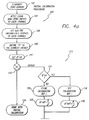
- Fig. 4a is a flow diagram of an illustrative calibration method for the system for matching the outputs of first and second analog-to-digital converters implemented in accordance with the teachings of the present invention.
- the calibration method 100 includes the steps of eliminating zero errors 102.
- step 104 equal nonzero inputs are applied to two of the three windings (channels) by the controller 30.
- the uncorrected outputs of the two channels are denoted as A and B.
- A is arbitrarily defined as the correct value.
- a parameter B' is set equal to B.
- the range of index i is set by a tradeoff between accuracy and speed.
- the routine 113 includes a decision step 114 which compares the value of B' to A. If B' is less than A, then at step 116, a calibration bit i is set. Then, at step 118, B' is incremented by B/2 i and the routine returns to step 114.
- step 114 If at step 114, B' is not less than A, then at step 120, the calibration bit is cleared and B' is decremented by B/2 i and the routine returns to step 114.
- step 124 the calibration of the system 10 is complete and the system goes to normal operational mode 200 depicted in Fig. 4b.
- Fig. 4b is a flow diagram of a normal method of operation for the system 10 of the present invention.
- a and B are denoted the uncalibrated outputs of each channel.
- a parameter A' is set equal to A and B' is set equal to B, respectively.
- the calibration bit is checked to determine if it has been set. If so, at step 212, B' is incremented by B/2 i and the routine returns to step 210. If the calibration bit is not set, at step 214, B' is decremented by B/2 i and the routine returns to step 218.
- A' and B' are the calibrated outputs.
Landscapes
- Engineering & Computer Science (AREA)
- Theoretical Computer Science (AREA)
- Analogue/Digital Conversion (AREA)
- Control Of Electric Motors In General (AREA)
Abstract
Description
- The present invention relates to analog-to-digital (A/D) converters. More specifically, the present invention relates to systems and methods for matching the outputs of two or more A/D converters.
- For many applications, there is a requirement to match the outputs of two or more A/D converters. One such application involves industrial motor control. Motors used in factories are typically servo-controlled and driven with three-phase currents. At one time, Hall effect sensors were used to measure the current flowing in the power lines feeding the motor. These devices allowed for the gain and offset to be manually controlled on each channel to optimized motor performance. Unfortunately, Hall effect devices are generaily large, heavy, expensive devices which are hard to solder onto a circuit board.
- Accordingly, isolated analog-to-digital converters and amplifiers were developed to replace Hall effect devices for motor control applications. While these devices were smaller and less expensive, they did not achieve the high gain matching performance of Hall effect devices.
- Subsequently, techniques were developed to improve the gain matching performance of the isolated A/D converters. One technique provided for an adjustment of an analog voltage on each of the chips that are performing an A/D conversion on each of the signal wires feeding voltage levels hack to a controller. However, this approach is expensive, requires manual adjustment after the unit is installed in the motor and is somewhat hazardous.
- Hence, a need remains in the art for an inexpensive system or technique for automatically matching outputs of A/D converters.
- The need in the art is addressed by the system and method for matching the outputs of first and second analog-to-digital converters of the present invention. In a most general sense, the inventive system includes a mechanism for sensing the output of the first converter and a mechanism for sensing the output of the second converter. A microprocessor runs software that computes a correction factor in response to the outputs of the first and second converters. The correction factor is used to adjust the output of the second converter to match the gain of the first converter in accordance with the needs of a particular application.
- In the illustrative embodiment, the correction factor is such that the gain of said second converter is equal to that of the first converter and the software includes code for adjusting the gain of the second converter to be greater than or equal to the output of the first converter. In the illustrative embodiment, the analog inputs to the A/D converters are provided by series sense resistors.
-
- Fig. 1 is a schematic/block diagram of an illustrative implementation of an application of a system for matching the gains of first and second analog-to-digital converters constructed in accordance with conventional teachings.
- Fig. 2 is a schematic/block diagram of an illustrative application of a system for matching the gains of first and second analog-to-digital converters constructed in accordance with the teachings of the present invention.
- Fig. 3 is block diagram of the isolated A/D converters of the system for matching the outputs of first and second analog-to-digital converters constructed in accordance with the teachings of the present invention.
- Fig. 4a is a flow diagram of a calibration method for the system for matching the outputs of first and second analog-to-digital converters implemented in accordance with the teachings of the present invention.
- Fig. 4b is a flow diagram of a normal method of operation for the system for matching the gains of first and second analog-to-digital converters implemented in accordance with the teachings of the present invention.
-
- Illustrative embodiments and exemplary applications will now be described with reference to the accompanying drawings to disclose the advantageous teachings of the present invention.
- While the present invention is described herein with reference to illustrative embodiments for particular applications, it should be understood that the invention is not limited thereto. Those having ordinary skill in the art and access to the teachings provided herein will recognize additional modifications, applications, and embodiments within the scope thereof and additional fields in which the present invention would be of significant utility.
- Fig. 1 is a schematic/block diagram of an illustrative implementation of an application of a system for matching the gains of first and second analog-to-digital converters constructed in accordance with conventional teachings. As shown in Fig. 1, in a typical motor drive system 10', current from a three-
phase source 12 is rectified to direct current (DC) by adiode rectifier circuit 14. The DC current is applied as a level adjusted, simulated, three-phase current to aninduction motor 20 via a plurality ofdrive transistors controller 30 supplies gate drive voltage to thedrive transistors gate drive circuits 22 and adjusts the level of same (and thereby the speed of the motor 20) via isolatedcurrent sensing circuits digital converters motor 20. - As mentioned above, the conventional implementation of Fig. 1, required an adjustment of the analog voltage on each of the chips performing the A/D conversions feeding back to the
controller 30. As this approach was expensive, required manual adjustment after the unit was installed in the motor and was somewhat hazardous, a need remained in the art for an inexpensive system or technique for automatically matching gains of A/D converters. - As discussed more fully below, the need in the art is addressed by the system and method for matching the gains of first and second analog-to-digital converters of the present invention.
- Fig. 2 is a schematic/block diagram of an illustrative application of a system for matching the gains of first and second analog-to-digital converters constructed in accordance with the teachings of the present invention. The
system 10 is similar to the system 10' of Fig. 1 with the exception that theinventive system 10 includesisolated modulators digital filters - Fig. 3 is block diagram showing the isolated modulator and A/D converter of Fig 2 in greater detail. The isolated modulators may be purchased from Hewlett Packard as HCPL 7860. As disclosed more fully in the attached data sheet, the
modulators ΣΔ modulator 44, anencoder 46 and alight emitting diode 48. The voltage sensed by themodulator 44 is converted to light by thediode 48. The light output by thediode 48 is sensed by adetector 50 and decoded by adecoder 52. The output of the decoder is the output of themodulator digital filter D converter 54. Theconverter 54 is programmable in response to a signal received from thecontroller 30. The digital filter may be purchased from Hewlett Packard as HCPL 7870. While those skilled in the art will understand how to effect microprocessor control of thefilters - Returning to Fig. 2, the
controller 30 receives and senses the ouputs of the first and second A/D converters second converters second converter 56 to match that of thefirst converter 54 in accordance with the needs of a particular application. - In operation, the method of the present invention takes advantage of the fact that in a 3-phase inverter motor drive with 2 phase current sensors, it is possible to deliver equal magnitude currents to the two sensors. This can be done by not turning on the 3rd phase, forcing all current to flow into phase (channel) 1 and out
phase 2. For a one-time factory calibration this current can be a DC current from an external power supply. For a power-up gain calibration this current can arise by applying a fixed voltage pulse acrossphases - By performing a simultaneous measurement on both phases, gain mismatch is evaluated. An offset calibration should be performed before gain calibration for best accuracy. By evaluating the gain mismatch, appropriate correction factors can be determined in a manner described below.
- Several methods are available for choosing the best correction values during the calibration phase.
- Fig. 4a is a flow diagram of an illustrative calibration method for the system for matching the outputs of first and second analog-to-digital converters implemented in accordance with the teachings of the present invention. The
calibration method 100 includes the steps of eliminating zeroerrors 102. Next, atstep 104, equal nonzero inputs are applied to two of the three windings (channels) by thecontroller 30. Atstep 106, the uncorrected outputs of the two channels are denoted as A and B. Atstep 108, A is arbitrarily defined as the correct value. Atstep 110, a parameter B' is set equal to B. - At step 112 a routine 113 is executed for a number of times i = 3 to 8. As will be appreciated by those of ordinary skill in he art, in practice, the range of index i is set by a tradeoff between accuracy and speed. The routine 113 includes a
decision step 114 which compares the value of B' to A. If B' is less than A, then atstep 116, a calibration bit i is set. Then, atstep 118, B' is incremented by B/2 i and the routine returns to step 114. - If at
step 114, B' is not less than A, then atstep 120, the calibration bit is cleared and B' is decremented by B/2 i and the routine returns to step 114. - At
step 124, the calibration of thesystem 10 is complete and the system goes to normaloperational mode 200 depicted in Fig. 4b. - Fig. 4b is a flow diagram of a normal method of operation for the
system 10 of the present invention. Atstep 202, A and B are denoted the uncalibrated outputs of each channel. Atsteps step 208, a routine 209 is executed for a number of times i = 3 to 8. Atstep 210, the calibration bit is checked to determine if it has been set. If so, atstep 212, B' is incremented by B/2 i and the routine returns to step 210. If the calibration bit is not set, atstep 214, B' is decremented by B/2 i and the routine returns to step 218. Atstep 218, A' and B' are the calibrated outputs. - These calibrated outputs compensate for gain errors in the A/
D converters motor 20 with balanced inputs. - Thus, the present invention has been described herein with reference to a particular embodiment for a particular application. Those having ordinary skill in the art and access to the present teachings will recognize additional modifications, applications and embodiments within the scope thereof.
- It is therefore intended by the appended claims to cover any and all such applications, modifications and embodiments within the scope of the present invention.
Claims (3)
- A system (10) for matching the outputs of first and second analog-to-digital converters (54) and (56) characterized by:a state machine (30) for sensing the outputs of the converters (54) and (56) and for computing a correction factor in response to the outputs of the first and second converters (54) and (56) anda mechanism responsive to the correction factor for adjusting the output of the second converter (56).
- The invention of Claim 1 wherein said correction factor is such that the gain of said second converter (56) is equal to that of the first converter (54).
- The invention of Claim 2 wherein said state machine includes code for adjusting the gain of the second converter (56) to be greater than or equal to the gain of the first converter (54).
Applications Claiming Priority (2)
| Application Number | Priority Date | Filing Date | Title |
|---|---|---|---|
| US38700599A | 1999-08-31 | 1999-08-31 | |
| US387005 | 1999-08-31 |
Publications (1)
| Publication Number | Publication Date |
|---|---|
| EP1081861A2 true EP1081861A2 (en) | 2001-03-07 |
Family
ID=23528035
Family Applications (1)
| Application Number | Title | Priority Date | Filing Date |
|---|---|---|---|
| EP20000116959 Withdrawn EP1081861A2 (en) | 1999-08-31 | 2000-08-07 | Gain calibration system and method for creating matched A/D converters |
Country Status (2)
| Country | Link |
|---|---|
| EP (1) | EP1081861A2 (en) |
| JP (1) | JP2001102924A (en) |
Cited By (2)
| Publication number | Priority date | Publication date | Assignee | Title |
|---|---|---|---|---|
| EP1280277A3 (en) * | 2001-07-12 | 2004-02-18 | Cirrus Logic, Inc. | Calibration of isolated analog-to-digital converters |
| CN113721178A (en) * | 2020-07-01 | 2021-11-30 | 镇江英创电力电子有限公司 | Full-automatic calibration method and system for high-voltage isolation transmitter |
-
2000
- 2000-08-07 EP EP20000116959 patent/EP1081861A2/en not_active Withdrawn
- 2000-08-23 JP JP2000253091A patent/JP2001102924A/en active Pending
Cited By (2)
| Publication number | Priority date | Publication date | Assignee | Title |
|---|---|---|---|---|
| EP1280277A3 (en) * | 2001-07-12 | 2004-02-18 | Cirrus Logic, Inc. | Calibration of isolated analog-to-digital converters |
| CN113721178A (en) * | 2020-07-01 | 2021-11-30 | 镇江英创电力电子有限公司 | Full-automatic calibration method and system for high-voltage isolation transmitter |
Also Published As
| Publication number | Publication date |
|---|---|
| JP2001102924A (en) | 2001-04-13 |
Similar Documents
| Publication | Publication Date | Title |
|---|---|---|
| US5012169A (en) | Motor drive system | |
| US7483279B2 (en) | Apparatus and method for detecting phase currents of inverter | |
| US11984808B2 (en) | Self-tuning regulator for interleaved power factor correction circuits and method of self-tuning regulation | |
| JP2727315B2 (en) | Insulation control method for injection molding machine | |
| JPH0744813B2 (en) | Position detector | |
| US20090040797A1 (en) | Pulse Width Modulation Method for a Power Converter | |
| US5619114A (en) | Signal averager for use with motor controller | |
| US6639810B2 (en) | Inverter apparatus for controlling a generator output to sign-wave voltage | |
| US5021724A (en) | Controlling apparatus for induction motor | |
| EP0427527B1 (en) | Offset correction circuit of PWM inverter | |
| EP0104909A2 (en) | Servomotor control method and apparatus therefor | |
| US20220260615A1 (en) | Apparatus and method for measuring a current flowing through a pwm-controlled inductive load | |
| US10608526B2 (en) | Device and method for calculating switching time | |
| JPH07170799A (en) | AC motor control method and device, and motor current correction method | |
| US5208524A (en) | Current control apparatus for PWM control | |
| JP2001102924A (en) | A / D converter gain matching system and matching method | |
| US11063546B2 (en) | Motor control device | |
| JPH08223920A (en) | Converter control method and apparatus, and converter AC current correction method used therefor | |
| KR101288196B1 (en) | Driving apparatus and method of motor with initial compensation | |
| KR940006963B1 (en) | Phase compensation method of synchronous AC servomotor | |
| JP3354633B2 (en) | Stepping motor drive | |
| US9529026B2 (en) | Angle detector, motor drive controller, and motor device | |
| JP2866361B2 (en) | Injection mechanism drive | |
| JP2003037989A (en) | Automatic phase adjuster for PM motor | |
| JP2005162462A (en) | Elevator control device |
Legal Events
| Date | Code | Title | Description |
|---|---|---|---|
| PUAI | Public reference made under article 153(3) epc to a published international application that has entered the european phase |
Free format text: ORIGINAL CODE: 0009012 |
|
| AK | Designated contracting states |
Kind code of ref document: A2 Designated state(s): AT BE CH CY DE DK ES FI FR GB GR IE IT LI LU MC NL PT SE |
|
| AX | Request for extension of the european patent |
Free format text: AL;LT;LV;MK;RO;SI |
|
| RAP1 | Party data changed (applicant data changed or rights of an application transferred) |
Owner name: AGILENT TECHNOLOGIES INC. |
|
| RAP1 | Party data changed (applicant data changed or rights of an application transferred) |
Owner name: AGILENT TECHNOLOGIES INC. A DELAWARE CORPORATION |
|
| RAP1 | Party data changed (applicant data changed or rights of an application transferred) |
Owner name: AGILENT TECHNOLOGIES, INC. (A DELAWARE CORPORATION |
|
| STAA | Information on the status of an ep patent application or granted ep patent |
Free format text: STATUS: THE APPLICATION HAS BEEN WITHDRAWN |
|
| 18W | Application withdrawn |
Withdrawal date: 20020829 |