EP1081841B1 - Arrangement de circuit pour un redresseur - Google Patents
Arrangement de circuit pour un redresseur Download PDFInfo
- Publication number
- EP1081841B1 EP1081841B1 EP20000118568 EP00118568A EP1081841B1 EP 1081841 B1 EP1081841 B1 EP 1081841B1 EP 20000118568 EP20000118568 EP 20000118568 EP 00118568 A EP00118568 A EP 00118568A EP 1081841 B1 EP1081841 B1 EP 1081841B1
- Authority
- EP
- European Patent Office
- Prior art keywords
- rectifier
- voltage
- power storage
- circuit
- control device
- Prior art date
- Legal status (The legal status is an assumption and is not a legal conclusion. Google has not performed a legal analysis and makes no representation as to the accuracy of the status listed.)
- Expired - Lifetime
Links
Images


Classifications
-
- H—ELECTRICITY
- H02—GENERATION; CONVERSION OR DISTRIBUTION OF ELECTRIC POWER
- H02M—APPARATUS FOR CONVERSION BETWEEN AC AND AC, BETWEEN AC AND DC, OR BETWEEN DC AND DC, AND FOR USE WITH MAINS OR SIMILAR POWER SUPPLY SYSTEMS; CONVERSION OF DC OR AC INPUT POWER INTO SURGE OUTPUT POWER; CONTROL OR REGULATION THEREOF
- H02M7/00—Conversion of ac power input into dc power output; Conversion of dc power input into ac power output
- H02M7/42—Conversion of dc power input into ac power output without possibility of reversal
- H02M7/44—Conversion of dc power input into ac power output without possibility of reversal by static converters
- H02M7/48—Conversion of dc power input into ac power output without possibility of reversal by static converters using discharge tubes with control electrode or semiconductor devices with control electrode
- H02M7/4826—Conversion of dc power input into ac power output without possibility of reversal by static converters using discharge tubes with control electrode or semiconductor devices with control electrode operating from a resonant DC source, i.e. the DC input voltage varies periodically, e.g. resonant DC-link inverters
-
- H—ELECTRICITY
- H02—GENERATION; CONVERSION OR DISTRIBUTION OF ELECTRIC POWER
- H02M—APPARATUS FOR CONVERSION BETWEEN AC AND AC, BETWEEN AC AND DC, OR BETWEEN DC AND DC, AND FOR USE WITH MAINS OR SIMILAR POWER SUPPLY SYSTEMS; CONVERSION OF DC OR AC INPUT POWER INTO SURGE OUTPUT POWER; CONTROL OR REGULATION THEREOF
- H02M7/00—Conversion of ac power input into dc power output; Conversion of dc power input into ac power output
- H02M7/02—Conversion of ac power input into dc power output without possibility of reversal
- H02M7/04—Conversion of ac power input into dc power output without possibility of reversal by static converters
- H02M7/12—Conversion of ac power input into dc power output without possibility of reversal by static converters using discharge tubes with control electrode or semiconductor devices with control electrode
- H02M7/21—Conversion of ac power input into dc power output without possibility of reversal by static converters using discharge tubes with control electrode or semiconductor devices with control electrode using devices of a triode or transistor type requiring continuous application of a control signal
- H02M7/217—Conversion of ac power input into dc power output without possibility of reversal by static converters using discharge tubes with control electrode or semiconductor devices with control electrode using devices of a triode or transistor type requiring continuous application of a control signal using semiconductor devices only
- H02M7/219—Conversion of ac power input into dc power output without possibility of reversal by static converters using discharge tubes with control electrode or semiconductor devices with control electrode using devices of a triode or transistor type requiring continuous application of a control signal using semiconductor devices only in a bridge configuration
Definitions
- the invention relates to a circuit arrangement for a rectifier consisting of a fed from a three-phase network, clocked by a control rectifier, the bridge branches each separately such controllable by the control device semiconductor switch and power diodes connected in parallel, that in the AC input of the rectifier sinusoidal currents flow and the DC link voltage is maintained at a constant value, wherein the rectifier is connected via a Kommut réellesvierpol with a capacitive intermediate circuit, which serves to supply a welding power source for the current of the welding process, the Kommutéesswierpol decoupling means for decoupling the rectifier output voltage from the intermediate circuit voltage, a clocked controlled by the control device inductive energy storage and a coupled with the controllable inductive energy storage discharge path au proves that in a first phase of the Kommutêtssenssenpols the rectifier output voltage is brought to zero by activation of the inductive energy storage, whereupon controlled by the controller switching on the semiconductor switch of the rectifier is energized, and that in a second phase of the
- Such a circuit is out of the US 5633793 bw. of the JP 10084674 known.
- the intermediate circuit voltage is stabilized and the currents flowing into the AC voltage input of the rectifier are ideally sinusoidal.
- control circuits for the alternating current and / or the DC link voltage are in the control unit provided, which are detected by a measuring device.
- the known solution is characterized in that the power switch of the rectifier bridge are always turned on only in such a time interval in which the voltage at the output of the rectifier is set to zero, so that corresponding circuit losses are avoided.
- the capacitive energy storage means also switching off the circuit breaker "softer".
- the invention is based on the object to improve the known device hinndtlid the efficiency range.
- the solution according to the invention consists in assigning to the decoupling means a switch unit controllable by the control device is such that an energy recovery from the DC voltage circuit into the AC system can be realized.
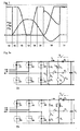
- FIG. 1 shows the circuit structure of an embodiment of a rectifier according to the invention arrangement.
- the circuit consists of one of a three-phase network UVW via input inductors L N fed rectifier, wherein the input inductors L N are preferably formed by network inductances, which consists of six bridge branches.
- the bridge branches in each case arranged parallel to each semiconductor switch S B1 -S B6, diodes D B1 -D B6 and capacitors C B1 -C B6.
- the semiconductor switches S B1 -S B6 are controllable by a control device ST, which receives as input the respective actual values of the input voltage V Nist and the input current I Nist of the three-phase network UVW.
- a Kommutêtsvierpol is arranged, which consists of the diodes D 1 -D 4 , the inductors L 2 , L R , the other capacitor C R and two other controllable semiconductor switches S R and S 2 .
- the further controllable semiconductor switches S R and S 2 are also controlled by the control device ST.
- the Kommut réellesvierpol consists of two shunt branches, of which a shunt branch is formed by a series circuit of the inductor L R and the other control switch S R.
- the further shunt branch of the commutation quadrupole is formed by the series connection of the two diodes D 1 , D 2 and the inductance L 2 arranged in series with the second diode D 2 .
- the two shunt arms are connected directly to each other via the further capacitor C R , wherein the center tap of the series circuit formed by the inductance L R and the semiconductor switch S R via a coupling diode D 4 with one connected to the Kommutêtsvierpol DC link capacitor is connected.
- a controllable semiconductor switch S 2 is arranged, which is controlled by the control device ST.
- the intermediate circuit voltage V 0 is also detected by the control device ST. From the DC link, an unillustrated consumer is supplied with electrical energy.
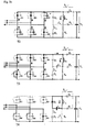
- Fig. 2 shows time waveforms, each divided into different time intervals T0-T7, for the output rectifier rectifier output voltage V B , for the current flowing through the inductor L R current I LR and over the other controllable semiconductor switch S R voltage V SR .
- FIGS. 3a to 3c include function diagrams associated with each of the periods T0-T7 to explain the operation of the circuit:
- the output voltage V B of the rectifier bridge is briefly brought to zero, so that at this time, the two switches S B4 and S B6 can be turned on in the de-energized state.
- the switches S B4 and S B6 can then be opened again, this being carried out according to the invention in a "switch-relieved" manner as described in more detail below.
- the initial state at time T0 is chosen so that the current through the diode D B1, D B2 B3 D and from the three-phase power flowing into the DC voltage circuit.
- the rectifier output voltage V B corresponds to the value of the intermediate circuit voltage V 0 .
- the current through the inductance L R is greater than the mains current I 0 , so that the diode D 3 is de-energized and the bridge capacitors C B4 , C B5 and C B6 are discharged.
- the switch S R is opened again and the capacitor C R is the current I LR , which is maximum at this time, charged until it is charged to the intermediate circuit voltage V 0 .
- the mains current in the rectifier bridge is short-circuited in freewheeling operation.
- the current I LR continues to flow through the inductance L R via the diode D 4 into the intermediate circuit and is reduced there.
- the maximum blocking voltage applied to the further semiconductor switch S R is simultaneously limited to the intermediate circuit voltage V 0 .
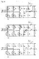
- Fig. 4 shows temporal current / voltage waveforms, each divided into different time intervals T0 - T7, for the voltage at the output of the rectifier V B , for the current flowing through the inductor L R current I LR and over the semiconductor switch S R voltage V SR .
- FIGS. 5a to 5c contain functional representations associated with each of the periods T0-T7 in order to explain the operation of the circuit:
- the output state at time T0 is selected so that the mains current via the switch S B2 and the diodes D B4 and D B6 is shorted.
- the switch S R is opened again and the capacitor C R is charged by the current I LR , which is the maximum at this time, up to the intermediate circuit voltage V 0 . In this case, the current in the inductance L R to zero.
- the switches S B1 and S B3 may be turned on at zero voltage during the time interval T3.
- the current I LR is greater than the mains current in the phase W.
- the charge of the capacitor C R flows back into the rectifier bridge, discharging the capacitor C R and the capacitors C B4 , C B5 B6 and C are loaded.
- the switch S 2 is closed.
- the voltage V B at the rectifier bridge is equal to the intermediate circuit voltage V 0 .
- the current I LR decreases and becomes zero.
Landscapes
- Engineering & Computer Science (AREA)
- Power Engineering (AREA)
- Rectifiers (AREA)
Claims (10)
- Agencement de circuit pour un redresseur constitué d'un redresseur alimenté par un réseau triphasé (U, V, W), synchronisé par un dispositif de commande (ST), dont les branches de pont présentent à chaque fois des interrupteurs à semi-conducteurs (SB1-SB6) pouvant être actionnés par le dispositif de commande (ST) et des diodes de puissance (DB1-DB6) branchées en parallèle, de telle sorte que des courants sinusoïdaux circulent dans l'entrée de tension alternative du redresseur et la tension du circuit intermédiaire (V0) est maintenue sur une valeur constante, le redresseur étant relié par un quadripôle de commutation à un circuit intermédiaire capacitif, lequel sert à l'alimentation d'un consommateur,
le quadripôle de commutation présentant des moyens de découplage (D3) pour le découplage de la tension de sortie de dresseur (VB) de la tension du circuit intermédiaire (Vo), un accumulateur d'énergie (LR, SR) inductif pouvant être actionné de façon synchronisée par le dispositif de commande (ST) et un chemin de décharge (CR, D1, D2, D4) couplé avec l'accumulateur d'énergie inductif actionnable, de telle sorte que, dans une première phase d'exploitation du quadripôle de commutation, la tension de sortie de redresseur (VB) est guidée par l'activation de l'accumulateur d'énergie (LR) inductif vers zéro, après quoi la mise en circuit, commandée par le dispositif de commande (ST), des interrupteurs à semi-conducteurs (SB1-SB6) du redresseur s'effectue sans tension, et en ce que, dans une seconde phase d'exploitation du quadripôle de commutation, l'énergie de l'accumulateur d'énergie (LR) inductif est transférée par une opération de transfert quasi résonante le long du chemin de décharge (CR, D1, D2, D4) dans des moyens d'accumulateur d'énergie (CB1-CB6) capacitifs, qui permettent à leur tour une déconnexion "souple" des semi-conducteurs de puissance (SB1-SB6),
caractérisé en ce qu'une unité de commutateur (S2) contrôlable par le dispositif de commande (ST) est attribuée aux moyens de découplage (D3), de telle sorte qu'une réjection d'énergie du circuit de tension continue dans le système de tension alternative est réalisable. - Agencement de circuit pour un redresseur selon la revendication 1,
caractérisé en ce que les moyens de découplage présentent au moins une diode de découplage (D3). - Agencement de circuit pour un redresseur selon la revendication 1 ou 2,
caractérisé en ce que l'accumulateur d'énergie inductif activable est formé par le montage en série constitué d'un interrupteur à semi-conducteurs (SR) commandé et d'une inductance (LR). - Agencement de circuit pour un redresseur selon la revendication 3,
caractérisé en ce que le montage en série est disposé dans une branche transversale du quadripôle de commutation. - Agencement de circuit pour un redresseur selon l'une quelconque des revendications précédentes,
caractérisé en ce que les moyens d'accumulateur d'énergie capacitifs sont formés par des condensateurs (CB1-CB6) disposés respectivement parallèlement aux interrupteurs à semi-conducteurs (SB1-SB6) contrôlables du redresseur. - Agencement de circuit pour un redresseur selon l'une quelconque des revendications précédentes,
caractérisé en ce que le chemin de décharge est formé par au moins deux diodes (D1, D2) disposées dans une autre branche transversale du quadripôle de commutation ainsi que par un condensateur (CR) disposé entre le point de raccordement commun des diodes et le point de raccordement commun de l'interrupteur à semi-conducteurs (SR) et de l'inductance (LR). - Agencement de circuit pour un redresseur selon la revendication 6,
caractérisé en ce que le condensateur (CR) est relié par une diode de couplage (D4) au circuit intermédiaire. - Agencement de circuit pour un redresseur selon l'une quelconque des revendications précédentes,
caractérisé en ce qu'une autre inductance (L2) est disposée en série avec l'une des au moins deux diodes (D2, D1). - Procédé pour l'exploitation d'un agencement de redresseur comprenant un redresseur alimenté par un réseau triphasé (U, V, W), synchronisé par un dispositif de commande (ST), dont des interrupteurs à semi-conducteurs (SB1-SB6) actionnables et des branches de pont présentant des diodes de puissance (DB1-DB6) commutées parallèlement à ces interrupteurs sont synchronisés à chaque fois séparément de telle sorte que des courants sinusoïdaux circulent dans l'entrée de tension alternative du redresseur et la tension de circuit intermédiaire (V0) est maintenue sur une valeur constante, le redresseur étant relié par un quadripôle de commutation à un circuit intermédiaire capacitif, lequel sert à l'alimentation d'un consommateur,
la tension de sortie de redresseur (VB) étant guidée vers zéro dans une première phase d'exploitation du quadripôle de commutation dissocié du circuit intermédiaire par une diode (D3) par l'activation d'un accumulateur d'énergie (LR) inductif, actionnable et synchronisé, après quoi la mise en circuit, commandée par le dispositif de commande (ST), des interrupteurs à semi-conducteurs (SB1-SB6) du redresseur s'effectue sans tension et en ce que, dans une seconde phase d'exploitation du quadripôle de commutation, l'énergie de l'accumulateur d'énergie (LR) inductif est transférée par une opération de transfert quasi résonante le long d'un chemin de décharge (CR, D1, D2, D4) dans des moyens d'accumulateur d'énergie (CB1-CB6) capacitifs, lesquels permettent à leur tour une mise hors circuit "souple" des interrupteurs de puissance (SB1-SB6),
caractérisé en ce qu'une réinjection d'énergie du circuit de tension continue dans le système de tension alternative peut être réalisée par l'attribution, en particulier par montage en parallèle, d'une unité de commutateur (S2) contrôlable par le dispositif de commande (ST) aux moyens de découplage. - Utilisation d'un dispositif selon l'une quelconque des revendications 1 à 9 pour l'alimentation d'une source de courant de soudage pour le courant d'un processus de soudage.
Applications Claiming Priority (2)
| Application Number | Priority Date | Filing Date | Title |
|---|---|---|---|
| DE1999142228 DE19942228A1 (de) | 1999-09-03 | 1999-09-03 | Schaltungsanordnung für einen aktiven Gleichrichter |
| DE19942228 | 1999-09-03 |
Publications (3)
| Publication Number | Publication Date |
|---|---|
| EP1081841A2 EP1081841A2 (fr) | 2001-03-07 |
| EP1081841A3 EP1081841A3 (fr) | 2004-12-08 |
| EP1081841B1 true EP1081841B1 (fr) | 2010-02-10 |
Family
ID=7920790
Family Applications (1)
| Application Number | Title | Priority Date | Filing Date |
|---|---|---|---|
| EP20000118568 Expired - Lifetime EP1081841B1 (fr) | 1999-09-03 | 2000-08-26 | Arrangement de circuit pour un redresseur |
Country Status (2)
| Country | Link |
|---|---|
| EP (1) | EP1081841B1 (fr) |
| DE (2) | DE19942228A1 (fr) |
Cited By (1)
| Publication number | Priority date | Publication date | Assignee | Title |
|---|---|---|---|---|
| RU2474034C2 (ru) * | 2011-03-29 | 2013-01-27 | Федеральное государственное бюджетное образовательное учреждение высшего профессионального образования Московский государственный технологический университет "СТАНКИН" (ФГБОУ ВПО МГТУ "СТАНКИН") | Двадцатичетырехпульсный преобразователь |
Families Citing this family (3)
| Publication number | Priority date | Publication date | Assignee | Title |
|---|---|---|---|---|
| DE102011001147A1 (de) * | 2011-03-08 | 2012-09-13 | Sma Solar Technology Ag | Vormagnetisierte AC-Drossel mit Polwender |
| RU189668U1 (ru) * | 2019-03-19 | 2019-05-30 | Евгений Борисович Колесников | Измерительный преобразователь трехфазного переменного напряжения в постоянное |
| DE102022211926A1 (de) | 2022-11-10 | 2024-05-16 | D + L Dubois + Linke Gesellschaft mit beschränkter Haftung | Schweißgerät |
Family Cites Families (3)
| Publication number | Priority date | Publication date | Assignee | Title |
|---|---|---|---|---|
| US5633793A (en) * | 1995-01-23 | 1997-05-27 | Center For Innovative Technology | Soft switched three-phase boost rectifiers and voltage source inverters |
| JP3315592B2 (ja) * | 1996-05-28 | 2002-08-19 | オリジン電気株式会社 | 昇圧形3相全波整流装置の制御方法及び制御回路 |
| JPH1084674A (ja) * | 1996-09-06 | 1998-03-31 | Sanken Electric Co Ltd | 交流−直流変換器 |
-
1999
- 1999-09-03 DE DE1999142228 patent/DE19942228A1/de not_active Withdrawn
-
2000
- 2000-08-26 EP EP20000118568 patent/EP1081841B1/fr not_active Expired - Lifetime
- 2000-08-26 DE DE50015863T patent/DE50015863D1/de not_active Expired - Lifetime
Cited By (1)
| Publication number | Priority date | Publication date | Assignee | Title |
|---|---|---|---|---|
| RU2474034C2 (ru) * | 2011-03-29 | 2013-01-27 | Федеральное государственное бюджетное образовательное учреждение высшего профессионального образования Московский государственный технологический университет "СТАНКИН" (ФГБОУ ВПО МГТУ "СТАНКИН") | Двадцатичетырехпульсный преобразователь |
Also Published As
| Publication number | Publication date |
|---|---|
| EP1081841A3 (fr) | 2004-12-08 |
| DE50015863D1 (de) | 2010-03-25 |
| DE19942228A1 (de) | 2001-03-08 |
| EP1081841A2 (fr) | 2001-03-07 |
Similar Documents
| Publication | Publication Date | Title |
|---|---|---|
| EP1145416B1 (fr) | Convertisseurs pour la transformation d'energie electrique | |
| EP1047180A2 (fr) | Convertisseur à trois-points ou à multi-points du type ARCP (Auxilliary Resonant Commutated Pole) | |
| EP1976108A2 (fr) | Convertisseur, en particulier pour une turbine à ions | |
| EP0951133A2 (fr) | Procédé et filtre actif pour réduire l'ondulation résiduelle d'un courant tiré d'un réseau par une charge | |
| EP2709257A2 (fr) | Circuit de convertisseur de courant et procédé de commande du circuit de convertisseur de courant | |
| DE112019001203T5 (de) | Energie-umwandlungseinrichtung | |
| EP1245074B1 (fr) | Systeme redresseur triphase a impulsions, a circuit intermediaire et a faible reaction sur le reseau, dote d'une large plage de reglage de la tension de sortie | |
| DE10238606B4 (de) | Schaltnetzteil | |
| DE2106310A1 (de) | Mehrphasen Leistungskonverterschaltung | |
| WO2003041248A2 (fr) | Transformateur de tension | |
| EP0087593B1 (fr) | Circuit pour installations de télécommunication, en particulier installations de centrale téléphonique avec convertisseurs continu-continu | |
| EP1081841B1 (fr) | Arrangement de circuit pour un redresseur | |
| DE4008652A1 (de) | Netzteil mit gleichstrom-gleichstrom-wandler | |
| EP3529102B1 (fr) | Convertisseur continu-continu et procédé pour opérer un convertisseur continu-continu | |
| EP0326681B1 (fr) | Appareil de soudage à l'arc pour l'alimentation en courant continu et alternatif | |
| EP1103330B1 (fr) | Appareil de coupage ou de soudage au plasma et méthode pour faire fonctionner un appareil de coupage ou de soudage au plasma | |
| DE60125336T2 (de) | Stromwandler mit wechselstrom- und gleichstrombetriebsmodus und verfahren zum betrieb desselben | |
| DE4325275A1 (de) | Stromrichterschaltung zur Speisung eines Gleichspannungszwischenkreises | |
| DE1638962A1 (de) | Stromkreis mit steuerbaren Gleichrichtern | |
| DE4430078A1 (de) | Schaltungsanordnung zur Vermeidung von Schaltverlusten eines Zweigpaares eines selbstgeführten Stromrichters mit eingeprägter Zwischenkreisgleichspannung | |
| DE3049020C2 (de) | Regelbarer Gleichspannungswandler für Leistungsschaltnetzteile | |
| DE19527178C1 (de) | Rückspeiseschaltung für eine Entlastungsschaltung für einen Zweipunkt- bzw. Dreipunkt-Ventilzweig | |
| DE4342414A1 (de) | Schaltungsanordnung zur Energieübertragung zwischen einem Gleichstrom- und einem Gleichspannungskreis und Verfahren zur Steuerung der Schaltung | |
| DE10159645B4 (de) | Verfahren und Vorrichtung zur Aufrechterhaltung einer Versorgungsspannung einer Stromversorgung einer Elektronik eines Matrixumrichters bei Netzunterbrechung | |
| DE3808433C1 (en) | Adjustable push-pull DC/DC converter and method for its control |
Legal Events
| Date | Code | Title | Description |
|---|---|---|---|
| PUAI | Public reference made under article 153(3) epc to a published international application that has entered the european phase |
Free format text: ORIGINAL CODE: 0009012 |
|
| AK | Designated contracting states |
Kind code of ref document: A2 Designated state(s): AT BE CH CY DE DK ES FI FR GB GR IE IT LI LU MC NL PT SE |
|
| AX | Request for extension of the european patent |
Free format text: AL;LT;LV;MK;RO;SI |
|
| PUAL | Search report despatched |
Free format text: ORIGINAL CODE: 0009013 |
|
| AK | Designated contracting states |
Kind code of ref document: A3 Designated state(s): AT BE CH CY DE DK ES FI FR GB GR IE IT LI LU MC NL PT SE |
|
| AX | Request for extension of the european patent |
Extension state: AL LT LV MK RO SI |
|
| 17P | Request for examination filed |
Effective date: 20050119 |
|
| AKX | Designation fees paid |
Designated state(s): DE FR IT |
|
| 17Q | First examination report despatched |
Effective date: 20080429 |
|
| GRAP | Despatch of communication of intention to grant a patent |
Free format text: ORIGINAL CODE: EPIDOSNIGR1 |
|
| GRAS | Grant fee paid |
Free format text: ORIGINAL CODE: EPIDOSNIGR3 |
|
| GRAA | (expected) grant |
Free format text: ORIGINAL CODE: 0009210 |
|
| AK | Designated contracting states |
Kind code of ref document: B1 Designated state(s): DE FR IT |
|
| REF | Corresponds to: |
Ref document number: 50015863 Country of ref document: DE Date of ref document: 20100325 Kind code of ref document: P |
|
| PLBE | No opposition filed within time limit |
Free format text: ORIGINAL CODE: 0009261 |
|
| STAA | Information on the status of an ep patent application or granted ep patent |
Free format text: STATUS: NO OPPOSITION FILED WITHIN TIME LIMIT |
|
| 26N | No opposition filed |
Effective date: 20101111 |
|
| PGFP | Annual fee paid to national office [announced via postgrant information from national office to epo] |
Ref country code: FR Payment date: 20110826 Year of fee payment: 12 Ref country code: DE Payment date: 20110817 Year of fee payment: 12 |
|
| PGFP | Annual fee paid to national office [announced via postgrant information from national office to epo] |
Ref country code: IT Payment date: 20110825 Year of fee payment: 12 |
|
| REG | Reference to a national code |
Ref country code: FR Ref legal event code: ST Effective date: 20130430 |
|
| PG25 | Lapsed in a contracting state [announced via postgrant information from national office to epo] |
Ref country code: IT Free format text: LAPSE BECAUSE OF NON-PAYMENT OF DUE FEES Effective date: 20120826 |
|
| PG25 | Lapsed in a contracting state [announced via postgrant information from national office to epo] |
Ref country code: DE Free format text: LAPSE BECAUSE OF NON-PAYMENT OF DUE FEES Effective date: 20130301 |
|
| PG25 | Lapsed in a contracting state [announced via postgrant information from national office to epo] |
Ref country code: FR Free format text: LAPSE BECAUSE OF NON-PAYMENT OF DUE FEES Effective date: 20120831 |
|
| REG | Reference to a national code |
Ref country code: DE Ref legal event code: R119 Ref document number: 50015863 Country of ref document: DE Effective date: 20130301 |