EP1081838A2 - Power control method and circuit, and power supply unit - Google Patents
Power control method and circuit, and power supply unit Download PDFInfo
- Publication number
- EP1081838A2 EP1081838A2 EP00302726A EP00302726A EP1081838A2 EP 1081838 A2 EP1081838 A2 EP 1081838A2 EP 00302726 A EP00302726 A EP 00302726A EP 00302726 A EP00302726 A EP 00302726A EP 1081838 A2 EP1081838 A2 EP 1081838A2
- Authority
- EP
- European Patent Office
- Prior art keywords
- output
- input
- adapter
- power supply
- control circuit
- Prior art date
- Legal status (The legal status is an assumption and is not a legal conclusion. Google has not performed a legal analysis and makes no representation as to the accuracy of the status listed.)
- Granted
Links
Images



Classifications
-
- H—ELECTRICITY
- H02—GENERATION; CONVERSION OR DISTRIBUTION OF ELECTRIC POWER
- H02M—APPARATUS FOR CONVERSION BETWEEN AC AND AC, BETWEEN AC AND DC, OR BETWEEN DC AND DC, AND FOR USE WITH MAINS OR SIMILAR POWER SUPPLY SYSTEMS; CONVERSION OF DC OR AC INPUT POWER INTO SURGE OUTPUT POWER; CONTROL OR REGULATION THEREOF
- H02M3/00—Conversion of DC power input into DC power output
- H02M3/22—Conversion of DC power input into DC power output with intermediate conversion into AC
- H02M3/24—Conversion of DC power input into DC power output with intermediate conversion into AC by static converters
- H02M3/28—Conversion of DC power input into DC power output with intermediate conversion into AC by static converters using discharge tubes with control electrode or semiconductor devices with control electrode to produce the intermediate AC
- H02M3/325—Conversion of DC power input into DC power output with intermediate conversion into AC by static converters using discharge tubes with control electrode or semiconductor devices with control electrode to produce the intermediate AC using devices of a triode or a transistor type requiring continuous application of a control signal
- H02M3/335—Conversion of DC power input into DC power output with intermediate conversion into AC by static converters using discharge tubes with control electrode or semiconductor devices with control electrode to produce the intermediate AC using devices of a triode or a transistor type requiring continuous application of a control signal using semiconductor devices only
- H02M3/33507—Conversion of DC power input into DC power output with intermediate conversion into AC by static converters using discharge tubes with control electrode or semiconductor devices with control electrode to produce the intermediate AC using devices of a triode or a transistor type requiring continuous application of a control signal using semiconductor devices only with automatic control of the output voltage or current, e.g. flyback converters
- H02M3/33523—Conversion of DC power input into DC power output with intermediate conversion into AC by static converters using discharge tubes with control electrode or semiconductor devices with control electrode to produce the intermediate AC using devices of a triode or a transistor type requiring continuous application of a control signal using semiconductor devices only with automatic control of the output voltage or current, e.g. flyback converters with galvanic isolation between input and output of both the power stage and the feedback loop
Definitions
- the present invention generally relates to power control methods and circuits and power supply units, and more particularly to a power control method and circuit and a power supply unit which can set a rated output.
- Electronic equipments such as portable or lap-top personal computers are designed so that it is possible to use a power supply unit such as an A.C. adapter as its power supply.
- the power supply unit is designed to satisfy a specification as a power supply, so that it is possible to supply a maximum power required by the electronic equipment.
- the power supply unit such as the A.C. adapter supplies a predetermined output voltage and a predetermined output current, which are referred to as a rated output.
- the power supply unit guarantees that a serviceable life of the power supply unit, a temperature rise of the power supply unit and the like are within predetermined tolerable ranges even if the power supply unit is continuously used at the rated output.
- circuits within the portable or lap-top personal computer are made up of various circuit elements, but not all of these circuit elements operate constantly.
- the operation of the portable or lap-top personal computer is dependent upon the application program which is activated, and the circuits which operate within the lap-top personal computer differ from time to time depending on the application program which runs.
- circuits related to a modem which connects the portable or lap-top personal computer to the telephone line operate, but the circuits related to the modem do not operate when the communication function is not used.
- circuits related to carrying out read and write with respect to a hard disk drive operate, but the circuits related to carrying out the read and write with respect to the hard disk drive do not operate when the program is carrying out numerical computations or is waiting for an input from an operator of the portable or lap-top personal computer.
- a power consumption of the portable or lap-top personal computer changes every moment depending on the operation of the program, and compared to a maximum power consumption, an average power consumption of the portable or lap-top personal computer is considerably low.
- the average power consumption is on the order of approximately one-half the maximum power consumption.
- the rated power under which the A.C. adapter can continuously operate depending on the actual state of the power consumption of the portable or lap-top personal computer as the rated output according to the specification of the A.C. adapter, so that it is possible to obtain from the A.C. adapter a power greater than the rated output for an extremely limited short time.
- the time for which the power greater than the rated output is used cannot be limited by the design of the portable or lap-top personal computer which uses the A.C. adapter.
- the power used by the portable or lap-top personal computer depends greatly on the operating application program and the manner in which the portable or lap-top personal computer is used. As a result, it is virtually impossible to guarantee that the time for which the power greater than the rated output is used will be limited to an extremely short time.
- the portable or lap-top personal computer uses an A.C. adapter of a type different from the A.C. adapter which is originally designed for use with the portable or lap-top personal computer, it is impossible to limit the time for which the power greater than the rated output is used to the extremely short time.
- the maximum power consumption of the electrical equipment which uses the power supply unit is obtained, by taking the above described problems into consideration, and the rated output of the power supply unit is set so that the power supply circuit within the power supply unit will not abnormally generate heat or break down even if the electronic equipment operates continuously for a long period of time at the maximum power consumption.
- This kind of power supply unit uses a switching regulator.
- embodiments of the present invention aim to provide a novel and useful power control method and circuit and power supply unit, in which the problems described above are eliminated.
- Another and more specific aim is to provide a power control method and circuit and a power supply unit, which can reduce the size, weight and cost of the power supply unit, guarantee stable and safe operation of the power supply unit, and sufficiently protect an electronic equipment which uses the power supply unit.
- Still another aim is to provide a power control method for controlling an output of a power supply comprising a setting step variably setting a maximum rated output based on a temperature.
- a power control method of the present invention an overload state exceeding a rated output is tolerated within a tolerable time, and a maximum tolerable rated output is reduced if the overload state continues for a time exceeding the tolerable time, so that an abnormal temperature rise of a power supply circuit can be positively prevented using a relatively simple construction.
- An input to the power supply may be an A.C. input or a D.C. input
- the power control method may further comprise a converting step converting the A.C. or D.C. input to a D.C. output different from said input.
- a converting step converting the A.C. or D.C. input to a D.C. output different from said input.
- a further aim of preferred embodiments is to provide a power control circuit for controlling an output of a power supply, comprising a setting section variably setting a maximum rated output based on input temperature information.
- a power control circuit of the present invention an overload state exceeding a rated output is tolerated within a tolerable time, and a maximum tolerable rated output is reduced if the overload state continues for a time exceeding the tolerable time, so that an abnormal temperature rise of a power supply circuit can be positively prevented using a relatively simple construction.
- Another aim of preferred embodiments is to provide a power supply unit which converts an A.C. or D.C. input from a power supply to a D.C. output different from said input, comprising a power control circuit variably setting a maximum rated output based on input temperature information.
- a power supply unit of the present invention an overload state exceeding a rated output is tolerated within a tolerable time, and a maximum tolerable rated output is reduced if the overload state continues for a time exceeding the tolerable time, so that an abnormal temperature rise of a power supply circuit can be positively prevented using a relatively simple construction.
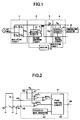
- FIG. 1 is a diagram showing a first embodiment of a power supply unit according to the present invention.
- This first embodiment of the power supply unit employs a first embodiment of a power control method according to the present invention and a first embodiment of a power control circuit according to the present invention.
- the present invention is applied to an A.C. adapter which converts an A.C. input into a D.C. output using a switching regulator.
- an A.C. adapter includes a rectifying circuit 1 for rectifying a commercial A.C. input, a voltage converter circuit 2 for converting the A.C. input obtained via the rectifying circuit 1 into a D.C. output having a different voltage, a rectifying circuit 3 for rectifying the D.C. output obtained via the voltage converter circuit 2, an output control circuit 4 for controlling the D.C. output obtained via the rectifying circuit 3, a coupler 5 for feeding back a state of the D.C. output obtained via the rectifying circuit 3 to the voltage converter circuit 2, and a temperature detector 6 for detecting a temperature within the A.C. adapter.
- the rectifying circuit 1 includes rectifying diodes D1 through D4, and a smoothing capacitor C1 for smoothing the rectified A.C. input, which are connected as shown in FIG. 1.
- the voltage converter circuit 2 includes a voltage converting transformer T1, a transistor Tr1 for switching ON/OFF a current flowing through the transformer T1, and a driving circuit 21 for controlling the ON/OFF state of the transistor Tr1, which are connected as shown in FIG. 1.
- the rectifying circuit 3 includes a rectifying diode D5, and a smoothing capacitor C2 for smoothing a D.C. output which is obtained from the voltage converter circuit 2 and is rectified by the rectifying diode D5, which are connected as shown in FIG. 1.
- the output control circuit 4 includes a sense resistor R0 for detecting the D.C. output obtained via the rectifying circuit 3, and a power control circuit 41 for controlling an output current and an output voltage of the A.C. adapter, which are connected as shown in FIG. 1.
- This power control circuit 41 forms a setting section for variably setting a maximum rated output of the A.C. adapter based on temperature information.
- the coupler 5 is made up of a known circuit which is provided to transmit a state of the output control on the secondary side of the transformer T1 of the voltage converter circuit 2 to the primary side of the transformer T1.
- This coupler 5 receives an output of the power control circuit 41.
- the coupler 5 uses a photo-coupler, for example.
- the temperature detector 6 obtains temperature information by detecting the temperature within the A.C. adapter, and supplies the temperature information to the power control circuit 41 within the output control circuit 4.
- the temperature detector 6 simply needs to be provided within the A.C. adapter, and the location of the temperature detector 6 is not limited to a specific location within the A.C. adapter. However, it is desirable to provide the temperature detector 6 within the A.C. adapter at a location where heat is generated when circuits operate, that is, in a vicinity of the power control circuit 41.
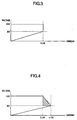
- FIG. 2 is a diagram showing an embodiment of the construction of the power control circuit 41 within the output control circuit 4 which is used in this first embodiment.
- the power control circuit 41 includes a voltage amplifier AMP1, error amplifiers ERA1 and ERA2, a triangular wave generator 42, a pulse width modulation (PWM) control circuit 43, and terminals 44 through 48 which are connected as shown in FIG. 2.
- the power control circuit 41 is formed by a single semiconductor integrated circuit device, that is, a single semiconductor chip. This semiconductor chip may also include circuit elements of the rectifying circuits 1 and 3 and/or the voltage converter circuit 2.
- the terminals 46 and 47 are respectively connected to terminals of the sense resistor R0, and to an inverting input terminal and a non-inverting input terminal of the voltage amplifier AMP1.
- the voltage amplifier AMP1 measures a voltage drop caused by a current flowing through the sense resistor R0, and outputs a voltage proportional to the current flowing through the sense resistor R0.
- the error amplifier ERA1 compares the output voltage of the voltage amplifier AMP1 input to the non-inverting input terminal and a reference voltage e3' input to the inverting input terminal, and inputs an output error voltage to the PWM control circuit 43.
- the reference voltage e3' input to the terminal 44 determines the output current of the A.C. adapter.
- This reference voltage e3' is obtained by voltage-dividing a reference voltage e3 from a reference voltage source e3 by a resistor R1 and a thermistor Th1.
- the error amplifier ERA2 compares a voltage from the terminal 47 input to the inverting input terminal and a reference voltage e2 from the terminal 45 input to the non-inverting input terminal, and inputs an output error voltage to the PWM control circuit 43.
- the reference voltage e2 input to the terminal 45 determines the output voltage of the A.C. adapter, and is obtained from a reference voltage source e2.
- the PWM control circuit 43 has two non-inverting input terminals respectively input with the output error voltages of the error amplifiers ERA1 and ERA2, and one inverting input terminal input with a triangular wave voltage from the triangular wave generator 42.
- the PWM control circuit 43 is a kind of voltage comparator, and controls an ON-time of an output pulse width depending on the input voltages.
- An output pulse voltage of the PWM control circuit 43 is output from the terminal 48 and is input to the coupler 5 shown in FIG. 1.
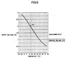
- the rated output of the A.C. adapter is 16 V/3.0 A, and the output voltage of 16 V is determined by the reference voltage e2, while the output current of 3.0 A is basically determined by the reference voltage e3'. If it were assumed for the sake of convenience that the reference voltage e3' were fixed, the rated output current is limited to 3.0 A if the load of the electronic equipment or the like connected to the A.C. adapter assumes an overload state which requires an output current exceeding 3.0 A, and the output voltage of the A.C. adapter would decrease. Because the output voltage of the A.C. adapter decreases, the abnormal heat generation from the A.C. adapter is prevented in the overload state.
- the A.C. adapter were able to continuously operate for more than a predetermined time in this region of the overload state, the A.C. adapter would abnormally generate heat.
- the ordinate indicates the output voltage of the A.C. adapter
- the abscissa indicates the output current of the A.C. adapter.
- the reference voltage e3' changes depending on the temperature within the A.C. adapter.
- the resistance of the thermistor Th1 changes depending on the temperature within the A.C. adapter. More particularly, the resistance of the thermistor Th1 becomes large when the temperature is low, and the resistance of the thermistor Th1 becomes small when the temperature is high.
- the reference voltage e3' which is obtained by voltage-dividing the reference voltage e3 by the resistor R1 and the thermistor Th1 becomes high when the temperature is low and becomes low when the temperature is high.
- FIG. 5 is a diagram showing the resistance of the thermistor Th1 which changes depending on the temperature. More particularly, FIG. 5 shows the changes in a resistance ThR and an output voltage ThO of the thermistor Th1 with respect to the temperature change.
- FIG. 6 is a diagram showing a change in the reference voltage e3' which determines the output current of the A.C. adapter, depending on the temperature change.
- the ordinate indicates the voltage
- the abscissa indicates the temperature.
- the error amplifier ERA1 outputs a low voltage if the voltage drop at the sense resistor R0 is larger when compared with the reference voltage e3', and outputs a high voltage if the voltage drop is smaller when compared with the reference voltage e3'.
- the error amplifier ERA2 outputs a low voltage if the voltage at the terminal of the sense resistor R0 connected to the terminal 47 is larger when compared with the reference voltage e2, and outputs a high voltage when the voltage at the terminal of the sense resistor R0 connected to the terminal 47 is smaller when compared with the reference voltage e2.
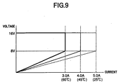
- an output characteristic of the A.C. adapter becomes as shown in FIG. 9.
- the ordinate indicates the output voltage of the A.C. adapter
- the abscissa indicates the output current of the A.C. adapter.
- the rated output of the A.C. adapter is set in this embodiment, so that the rated output voltage is 16 V and the rated output current is 3.0 A.
- FIG. 9 indicates that the continuous operation of the A.C. adapter is guaranteed at this rated output, even when the temperature within the A.C. adapter is 60°C.
- this embodiment can tolerate a maximum rated current of up to 5.0 A, as the maximum rated output exceeding the rated output.
- the maximum rated current which is tolerable with respect to the overload decreases to 4.0 A, so as to operate the A.C. adapter in a direction so as to decrease the temperature within the A.C. adapter. If the overload state of the A.C. adapter is eliminated in this state, the temperature rise within the A.C. adapter stops.
- the maximum rated current is variably set depending on the temperature within the A.C. adapter. Hence, even if the overload state exceeding the rated current continues within a tolerable time, the maximum rated current of the A.C. adapter is maintained. On the other hand, if the overload state continues exceeding the tolerable time, the maximum rated current is automatically decreased, so that the temperature within the A.C. adapter will not increase abnormally.
- the thermistor Th1 is used as the temperature detector 6.
- the temperature detector 6 is of course not limited to the thermistor Th1, and any suitable element or device capable of detecting the temperature may be used as the temperature detector 6.
- a thermocouple which uses the Seebeck effect may be used as the temperature detector 6.
- This second embodiment of the power supply unit employs a second embodiment of the power control method according to the present invention and a second embodiment of the power control circuit according to the present invention.
- the present invention is also applied to an A.C. adapter which converts an A.C. input into a D.C. output using a switching regulator.
- this second embodiment of the power supply unit is the same as that of the first embodiment shown in FIG. 1, and a description and illustration thereof will be omitted.
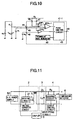
- a power control circuit 41-1 shown in FIG. 10 is used in place of the power control circuit 41 shown in FIG. 2.
- those parts which are the same as those corresponding parts in FIG. 2 are designated by the same reference numerals, and a description thereof will be omitted.
- the power control circuit 41-1 of this second embodiment further includes a terminal 49, and uses a 3-input error amplifier ERA1-1 in place of the error amplifier ERA1 shown in FIG. 2.
- a reference voltage e1 is input to the terminal 49, and this reference voltage e1 is input to a second non-inverting input terminal of the error amplifier ERA1-1.
- the reference voltage e3' is used for the comparison with the output voltage of the voltage amplifier AMP1 when the reference voltage e3' is lower than the reference voltage e1
- the reference voltage e1 is used for the comparison with the output voltage of the voltage amplifier AMP1 when the reference voltage e3' is higher than the reference voltage e1.
- the output voltage of the voltage amplifier AMP1 which generates a voltage proportional to the current flowing through the sense resistor R0 is input to the inverting input terminal of the error amplifier ERA1-1.
- the output current dependent on the reference voltages input to the non-inverting input terminals of the error amplifier ERA1-1 becomes the output current of the A.C. adapter.
- the maximum rated output current usable exceeding the rated output current of the A.C. adapter becomes large, but it limited to a current determined by the reference voltage e1 at a certain temperature.
- the reference voltage e3' decreases with the temperature rise, and the output voltage of the A.C. adapter is limited based on the reference voltage e3', thereby making the maximum rated output current of the A.C. adapter small. Consequently, the output characteristic of the A.C. adapter becomes as shown in FIG. 9, similarly to the first embodiment described above.
- This third embodiment of the power supply unit employs a third embodiment of the power control method according to the present invention and a third embodiment of the power control circuit according to the present invention.
- the present invention is applied to a D.C. adapter which converts a D.C. input to a D.C. output different from the D.C. input.
- FIG. 11 is a diagram showing the third embodiment of the power supply unit.
- the D.C. input is obtained from a D.C. power supply 50 such as an automobile battery.
- This D.C. input is input directly to the voltage converter circuit 2.
- a D.C. output different from the D.C. input is obtained form the output control circuit 4.
- this third embodiment basically has the same construction as the first embodiment described above, except that the rectifying circuit 1 shown in FIG. 1 is omitted in this third embodiment.
Landscapes
- Engineering & Computer Science (AREA)
- Power Engineering (AREA)
- Dc-Dc Converters (AREA)
- Control Of Voltage And Current In General (AREA)
- Rectifiers (AREA)
- Emergency Protection Circuit Devices (AREA)
Abstract
Description
Claims (11)
- A power control method for controlling an output of a power supply characterized by:a setting step variably setting a maximum rated output based on a temperature.
- The power control method as claimed in claim 1, wherein an input to the power supply is an A.C. input or a D.C. input, and further characterized by:a converting step converting the A.C. or D.C. input to a D.C. output different from said input.
- The power control method as claimed in claim 1 or 2, characterized in that said setting step variably sets a maximum rated current based on the temperature.
- A power control circuit for controlling an output of a power supply, characterized by:a setting section variably setting a maximum rated output based on input temperature information.
- The power control circuit as claimed in claim 4, wherein an input to the power supply is an A.C. input or a D.C. input, and further characterized by:a control circuit converting the A.C. or D.C. input to a D.C. output different from said input.
- The power control circuit as claimed in claim 4 or 5, characterized in that said setting section variably sets a maximum rated current based on the input temperature information.
- The power control circuit as claimed in claim 4, characterized in that said setting section variably sets the maximum rated output based on the input temperature information and reference information, said reference information indicating a rated value of an output current and/or an output voltage.
- A power supply unit which converts an A.C. or D.C. input from a power supply to a D.C. output different from said input, characterized by:a power control circuit variably setting a maximum rated output based on input temperature information.
- The power supply unit as claimed in claim 8, characterized in that said power control circuit variably sets a maximum rated current based on the input temperature information.
- The power supply unit as claimed in claim 8, characterized in that said power control circuit variably sets the maximum rated output based on the input temperature information and reference information, said reference information indicating a rated value of an output current and/or an output voltage of the power control circuit.
- The power supply unit as claimed in any of claims 8 to 10, further characterized by:a temperature detector detecting a temperature and inputting the input temperature information to said power control circuit.
Applications Claiming Priority (2)
| Application Number | Priority Date | Filing Date | Title |
|---|---|---|---|
| JP24638999A JP3642398B2 (en) | 1999-08-31 | 1999-08-31 | Power supply control method, circuit and power supply device |
| JP24638999 | 1999-08-31 |
Publications (3)
| Publication Number | Publication Date |
|---|---|
| EP1081838A2 true EP1081838A2 (en) | 2001-03-07 |
| EP1081838A3 EP1081838A3 (en) | 2001-03-21 |
| EP1081838B1 EP1081838B1 (en) | 2005-06-01 |
Family
ID=17147813
Family Applications (1)
| Application Number | Title | Priority Date | Filing Date |
|---|---|---|---|
| EP00302726A Expired - Lifetime EP1081838B1 (en) | 1999-08-31 | 2000-03-31 | Power control method and circuit, and power supply unit |
Country Status (5)
| Country | Link |
|---|---|
| US (1) | US6366475B2 (en) |
| EP (1) | EP1081838B1 (en) |
| JP (1) | JP3642398B2 (en) |
| CN (2) | CN101242140B (en) |
| DE (1) | DE60020464T2 (en) |
Families Citing this family (23)
| Publication number | Priority date | Publication date | Assignee | Title |
|---|---|---|---|---|
| JP3944605B2 (en) * | 2002-09-30 | 2007-07-11 | ローム株式会社 | Switching power supply |
| JP2005074768A (en) * | 2003-08-29 | 2005-03-24 | Brother Ind Ltd | Tape printer |
| JP4523330B2 (en) * | 2004-05-11 | 2010-08-11 | 株式会社リコー | Power supply circuit and equipment having the power supply circuit |
| JPWO2006101135A1 (en) | 2005-03-22 | 2008-09-04 | 沖パワーテック株式会社 | Switching power supply circuit |
| JP4882482B2 (en) * | 2006-04-24 | 2012-02-22 | パナソニック株式会社 | Power supply |
| KR100799836B1 (en) | 2006-09-11 | 2008-01-31 | 삼성전기주식회사 | Output Compensation Circuit Insensitive to Temperature Change |
| JP5057928B2 (en) * | 2007-10-19 | 2012-10-24 | 三洋電機株式会社 | Power system |
| JP5288446B2 (en) * | 2008-03-18 | 2013-09-11 | Necアクセステクニカ株式会社 | Electronic device system and power control method thereof |
| JP2010067294A (en) * | 2008-09-09 | 2010-03-25 | Toshiba Storage Device Corp | Magnetic disk device |
| JP5430105B2 (en) * | 2008-09-18 | 2014-02-26 | パナソニック株式会社 | Power supply system |
| JP2011114984A (en) * | 2009-11-27 | 2011-06-09 | Sanyo Electric Co Ltd | Switching control circuit, and power supply apparatus |
| JP2013113867A (en) * | 2011-11-25 | 2013-06-10 | Konica Minolta Business Technologies Inc | Image forming apparatus |
| WO2014019860A2 (en) * | 2012-08-03 | 2014-02-06 | Abb Technology Ag | Overload limitation in peak power operation |
| WO2014024244A1 (en) | 2012-08-06 | 2014-02-13 | 富士通株式会社 | Power supply circuit, electronic processing device, and power supply method |
| TWI474592B (en) * | 2013-04-29 | 2015-02-21 | Chicony Power Tech Co Ltd | Bypass apparatus for negative temperature coefficient thermistor |
| CN104093238B (en) * | 2014-06-24 | 2016-05-11 | 苏州达方电子有限公司 | In the time of high temperature, can reduce the power supply changeover device of light emitting diode drive current |
| JP2018136707A (en) | 2017-02-21 | 2018-08-30 | 富士通株式会社 | Power supply unit |
| CN111034000B (en) * | 2017-09-06 | 2023-04-18 | 株式会社日立产机系统 | Power conversion device |
| US11262832B2 (en) * | 2018-03-19 | 2022-03-01 | Hewlett-Packard Development Company, L.P. | Power consumption control of computing devices |
| CN113098343B (en) * | 2021-04-15 | 2023-11-21 | 深圳市正浩创新科技股份有限公司 | Generator output power control method, device, system and electronic equipment |
| BE1029972B1 (en) * | 2021-12-17 | 2023-10-18 | Atlas Copco Airpower Nv | METHOD OF CONTROLLING ELECTRICAL SUPPLY FOR A MAGNETIC BEARING CONTROL SYSTEM |
| CN114625201B (en) * | 2022-03-08 | 2024-12-06 | 成都芯源系统有限公司 | Control circuit and control method of voltage regulator |
| CN117293938A (en) * | 2022-06-17 | 2023-12-26 | 上海韦尔半导体股份有限公司 | power supply system |
Family Cites Families (12)
| Publication number | Priority date | Publication date | Assignee | Title |
|---|---|---|---|---|
| US4672226A (en) * | 1985-03-08 | 1987-06-09 | Westinghouse Electric Corp. | Redundant resistance temperature detector power supply system |
| US4777575A (en) | 1986-03-25 | 1988-10-11 | Hitachi Ltd. | Switching power supply |
| JPS6419966A (en) | 1987-07-10 | 1989-01-24 | Canon Kk | Switching regulator |
| JPH0371589A (en) * | 1989-08-10 | 1991-03-27 | Toshiba Corp | Microwave range |
| JPH04168973A (en) | 1990-10-31 | 1992-06-17 | Toshiba Corp | Power supply circuit and driving circuit employing said power supply circuit |
| US5157594A (en) * | 1991-09-16 | 1992-10-20 | Sundstrand Corporation | Temperature-based inverter control system |
| US5373205A (en) * | 1992-12-29 | 1994-12-13 | Cincinnati Milacron Inc. | Method and apparatus for limiting motor current |
| JPH07107619A (en) | 1993-09-29 | 1995-04-21 | Nippondenso Co Ltd | Auxiliary battery charger for electric automobile |
| JP2704132B2 (en) | 1995-05-22 | 1998-01-26 | 福島日本電気株式会社 | Switching power supply |
| JPH09163588A (en) * | 1995-12-06 | 1997-06-20 | Oki Data:Kk | Power supply circuit |
| US5690849A (en) * | 1996-02-27 | 1997-11-25 | Thermotek, Inc. | Current control circuit for improved power application and control of thermoelectric devices |
| JPH1118430A (en) | 1997-06-25 | 1999-01-22 | Nec Yonezawa Ltd | Temperature failure detection protection circuit |
-
1999
- 1999-08-31 JP JP24638999A patent/JP3642398B2/en not_active Expired - Fee Related
-
2000
- 2000-03-27 US US09/535,983 patent/US6366475B2/en not_active Expired - Lifetime
- 2000-03-31 DE DE60020464T patent/DE60020464T2/en not_active Expired - Lifetime
- 2000-03-31 EP EP00302726A patent/EP1081838B1/en not_active Expired - Lifetime
- 2000-04-21 CN CN2008100094639A patent/CN101242140B/en not_active Expired - Fee Related
- 2000-04-21 CN CNB001069152A patent/CN100544173C/en not_active Expired - Fee Related
Also Published As
| Publication number | Publication date |
|---|---|
| CN100544173C (en) | 2009-09-23 |
| JP2001075659A (en) | 2001-03-23 |
| DE60020464T2 (en) | 2005-10-27 |
| US6366475B2 (en) | 2002-04-02 |
| CN101242140B (en) | 2012-02-15 |
| EP1081838A3 (en) | 2001-03-21 |
| EP1081838B1 (en) | 2005-06-01 |
| DE60020464D1 (en) | 2005-07-07 |
| CN101242140A (en) | 2008-08-13 |
| JP3642398B2 (en) | 2005-04-27 |
| US20020015316A1 (en) | 2002-02-07 |
| CN1291820A (en) | 2001-04-18 |
Similar Documents
| Publication | Publication Date | Title |
|---|---|---|
| US6366475B2 (en) | Power control method and circuit, and power supply unit | |
| US6950950B2 (en) | Technique for conveying overload conditions from an AC adapter to a load powered by the adapter | |
| US6094362A (en) | Switched-mode power converter with triple protection in a single latch | |
| US8559200B2 (en) | Method and apparatus of low current startup circuit for switching mode power supplies | |
| EP2060963B1 (en) | Systems and methods for controlling use of power in a computer system | |
| US7755337B2 (en) | Current sensing circuit and voltage regulator using the same | |
| US7068485B2 (en) | Multi-output electric power source device and vehicle-mounted electronic control device | |
| JP7368132B2 (en) | series regulator | |
| US9621054B2 (en) | Power supply circuit, electronic processing apparatus, and power supply method | |
| JP4487620B2 (en) | Switching power supply | |
| US11860597B2 (en) | Smart switch system | |
| CN114365368A (en) | Overcurrent protection circuit | |
| US7405545B2 (en) | Voltage-regulator and power supply having current sharing circuit | |
| CN205566078U (en) | Information -processing device | |
| US5903182A (en) | Method and system for providing a regulated core voltage to a processor within a computer system | |
| JP3099763B2 (en) | DC power supply | |
| CN100372207C (en) | Parallel power supply combined with active-falling current distribution circuit | |
| US12424921B2 (en) | Power supply controller circuit for effectively saving power under electrical specification | |
| JP2021040364A (en) | Power supply circuit | |
| US20250015588A1 (en) | Power supply unit and control method of power supply unit | |
| JP2024099139A (en) | Switching Power Supply Unit | |
| JP2002320387A (en) | Power supply circuit |
Legal Events
| Date | Code | Title | Description |
|---|---|---|---|
| PUAI | Public reference made under article 153(3) epc to a published international application that has entered the european phase |
Free format text: ORIGINAL CODE: 0009012 |
|
| PUAL | Search report despatched |
Free format text: ORIGINAL CODE: 0009013 |
|
| AK | Designated contracting states |
Kind code of ref document: A2 Designated state(s): DE FR GB |
|
| AX | Request for extension of the european patent |
Free format text: AL;LT;LV;MK;RO;SI |
|
| AK | Designated contracting states |
Kind code of ref document: A3 Designated state(s): AT BE CH CY DE DK ES FI FR GB GR IE IT LI LU MC NL PT SE |
|
| AX | Request for extension of the european patent |
Free format text: AL;LT;LV;MK;RO;SI |
|
| 17P | Request for examination filed |
Effective date: 20010411 |
|
| AKX | Designation fees paid |
Free format text: DE FR GB |
|
| 17Q | First examination report despatched |
Effective date: 20020823 |
|
| GRAP | Despatch of communication of intention to grant a patent |
Free format text: ORIGINAL CODE: EPIDOSNIGR1 |
|
| GRAS | Grant fee paid |
Free format text: ORIGINAL CODE: EPIDOSNIGR3 |
|
| GRAA | (expected) grant |
Free format text: ORIGINAL CODE: 0009210 |
|
| AK | Designated contracting states |
Kind code of ref document: B1 Designated state(s): DE FR GB |
|
| REG | Reference to a national code |
Ref country code: GB Ref legal event code: FG4D |
|
| RIN1 | Information on inventor provided before grant (corrected) |
Inventor name: OZAWA, HIDEKIYO,C/O FUJITSU LIMITED Inventor name: YANO, HIDETOSHI,C/O FUJITSU LIMITED Inventor name: NAKAZAWA, SHIGEAKI,C/O FUJITSU LIMITED Inventor name: TANAKA, SHIGEO,C/O FUJITSU LIMITED |
|
| REF | Corresponds to: |
Ref document number: 60020464 Country of ref document: DE Date of ref document: 20050707 Kind code of ref document: P |
|
| ET | Fr: translation filed | ||
| PLBE | No opposition filed within time limit |
Free format text: ORIGINAL CODE: 0009261 |
|
| STAA | Information on the status of an ep patent application or granted ep patent |
Free format text: STATUS: NO OPPOSITION FILED WITHIN TIME LIMIT |
|
| 26N | No opposition filed |
Effective date: 20060302 |
|
| REG | Reference to a national code |
Ref country code: FR Ref legal event code: PLFP Year of fee payment: 17 |
|
| REG | Reference to a national code |
Ref country code: FR Ref legal event code: PLFP Year of fee payment: 18 |
|
| REG | Reference to a national code |
Ref country code: FR Ref legal event code: PLFP Year of fee payment: 19 |
|
| PGFP | Annual fee paid to national office [announced via postgrant information from national office to epo] |
Ref country code: DE Payment date: 20180320 Year of fee payment: 19 Ref country code: GB Payment date: 20180329 Year of fee payment: 19 |
|
| PGFP | Annual fee paid to national office [announced via postgrant information from national office to epo] |
Ref country code: FR Payment date: 20180223 Year of fee payment: 19 |
|
| REG | Reference to a national code |
Ref country code: DE Ref legal event code: R081 Ref document number: 60020464 Country of ref document: DE Owner name: FUJITSU CLIENT COMPUTING LIMITED, KAWASAKI-SHI, JP Free format text: FORMER OWNER: FUJITSU LIMITED, KAWASAKI-SHI, KANAGAWA, JP Ref country code: DE Ref legal event code: R082 Ref document number: 60020464 Country of ref document: DE Representative=s name: REICHERT & LINDNER PARTNERSCHAFT PATENTANWAELT, DE |
|
| REG | Reference to a national code |
Ref country code: GB Ref legal event code: 732E Free format text: REGISTERED BETWEEN 20190207 AND 20190213 |
|
| REG | Reference to a national code |
Ref country code: DE Ref legal event code: R119 Ref document number: 60020464 Country of ref document: DE |
|
| GBPC | Gb: european patent ceased through non-payment of renewal fee |
Effective date: 20190331 |
|
| PG25 | Lapsed in a contracting state [announced via postgrant information from national office to epo] |
Ref country code: GB Free format text: LAPSE BECAUSE OF NON-PAYMENT OF DUE FEES Effective date: 20190331 Ref country code: DE Free format text: LAPSE BECAUSE OF NON-PAYMENT OF DUE FEES Effective date: 20191001 |
|
| PG25 | Lapsed in a contracting state [announced via postgrant information from national office to epo] |
Ref country code: FR Free format text: LAPSE BECAUSE OF NON-PAYMENT OF DUE FEES Effective date: 20190331 |