EP1081833B1 - Power converter apparatus - Google Patents
Power converter apparatus Download PDFInfo
- Publication number
- EP1081833B1 EP1081833B1 EP00119313A EP00119313A EP1081833B1 EP 1081833 B1 EP1081833 B1 EP 1081833B1 EP 00119313 A EP00119313 A EP 00119313A EP 00119313 A EP00119313 A EP 00119313A EP 1081833 B1 EP1081833 B1 EP 1081833B1
- Authority
- EP
- European Patent Office
- Prior art keywords
- diode
- capacitor
- snubber
- cooler
- semiconductor
- Prior art date
- Legal status (The legal status is an assumption and is not a legal conclusion. Google has not performed a legal analysis and makes no representation as to the accuracy of the status listed.)
- Expired - Lifetime
Links
- 239000004065 semiconductor Substances 0.000 claims description 101
- 239000003990 capacitor Substances 0.000 claims description 38
- 230000007935 neutral effect Effects 0.000 claims description 29
- 230000004907 flux Effects 0.000 claims description 14
- 238000001816 cooling Methods 0.000 description 40
- 230000001052 transient effect Effects 0.000 description 8
- 230000000452 restraining effect Effects 0.000 description 5
- 238000010586 diagram Methods 0.000 description 4
- 239000000853 adhesive Substances 0.000 description 3
- 230000001070 adhesive effect Effects 0.000 description 3
- 230000000694 effects Effects 0.000 description 3
- 239000012212 insulator Substances 0.000 description 3
- 125000006850 spacer group Chemical group 0.000 description 3
- 238000009499 grossing Methods 0.000 description 2
- 230000008646 thermal stress Effects 0.000 description 2
- 229910001369 Brass Inorganic materials 0.000 description 1
- 239000004593 Epoxy Substances 0.000 description 1
- 230000015572 biosynthetic process Effects 0.000 description 1
- 239000010951 brass Substances 0.000 description 1
- 238000010276 construction Methods 0.000 description 1
- 230000008602 contraction Effects 0.000 description 1
- 238000002347 injection Methods 0.000 description 1
- 239000007924 injection Substances 0.000 description 1
- 239000008188 pellet Substances 0.000 description 1
- XLYOFNOQVPJJNP-UHFFFAOYSA-N water Substances O XLYOFNOQVPJJNP-UHFFFAOYSA-N 0.000 description 1
Images




Classifications
-
- H—ELECTRICITY
- H02—GENERATION; CONVERSION OR DISTRIBUTION OF ELECTRIC POWER
- H02M—APPARATUS FOR CONVERSION BETWEEN AC AND AC, BETWEEN AC AND DC, OR BETWEEN DC AND DC, AND FOR USE WITH MAINS OR SIMILAR POWER SUPPLY SYSTEMS; CONVERSION OF DC OR AC INPUT POWER INTO SURGE OUTPUT POWER; CONTROL OR REGULATION THEREOF
- H02M7/00—Conversion of AC power input into DC power output; Conversion of DC power input into AC power output
- H02M7/42—Conversion of DC power input into AC power output without possibility of reversal
- H02M7/44—Conversion of DC power input into AC power output without possibility of reversal by static converters
- H02M7/48—Conversion of DC power input into AC power output without possibility of reversal by static converters using discharge tubes with control electrode or semiconductor devices with control electrode
-
- H—ELECTRICITY
- H02—GENERATION; CONVERSION OR DISTRIBUTION OF ELECTRIC POWER
- H02M—APPARATUS FOR CONVERSION BETWEEN AC AND AC, BETWEEN AC AND DC, OR BETWEEN DC AND DC, AND FOR USE WITH MAINS OR SIMILAR POWER SUPPLY SYSTEMS; CONVERSION OF DC OR AC INPUT POWER INTO SURGE OUTPUT POWER; CONTROL OR REGULATION THEREOF
- H02M1/00—Details of apparatus for conversion
- H02M1/12—Arrangements for reducing harmonics from AC input or output
Definitions
- This invention relates to a power converter apparatus that uses high-speed semiconductor switching devices and includes a snubber circuit for restraining a surge voltage, and especially to a wiring structure of the snubber citcuit.
- GCT Gate-communicated Thyristor
- IGBT Insulated Gate Bipolar Transistor
- IEGT Injection Enhanced Gate Transistor
- These high-speed semiconductor switching devices which are capable of switching a voltage of 3-6 KV (Kilo-Volts) and a current of 3-4 KA (Kilo-Amperes), have been developed and made practical. Further, since a dV/dt resistance of a semiconductor switching device at a time of turning off has been improved, it is attempted that a snubber circuit is made smaller in size and less loss.
- FIG. 1 is a circuit diagram showing a conventional NPC (Neutral Point Clamped) inverter that uses GTO (Gate Turn-off Thyristor) as a semiconductor switching device.
- Snubber circuits 2a, 3a, 4a and 5a are respectively connected to GTO switching devices 2, 3, 4 and 5.
- Each of the snubber circuits 2a-5a restrains a surge voltage generated at switching the GTO switching devices 2-5 and includes a capacitor, a diode and a resistor.
- JP 09285136 there is disclosed a power converter apparatus comprising an inverter converting a Dc input voltage into three phase output AC voltage comprising stacked semiconductors, cooling means and snubber circuits with capacitors, diodes and resistors and a cooling system.
- JP 08069893 there is disclosed restraining a surge voltage in order to prevent the rupture of a switch by connecting a laminated plate to reduce the inductance of a wiring between a DC power source and an inverter.
- one object of this invention is to provide a power converter apparatus which may reduce a surge voltage generated at switching a semiconductor switching device and protect the semiconductor switching device from the surge voltage.
- a power converter apparatus comprising: a DC power source; a semiconductor stack, connected to said DC power source in parallel, having a plurality of semiconductor devices and a cooler for refrigerating said semiconductor devices, said semiconductor devices and said cooler are stacked and pressured to each other; and a snubber circuit, connected to said DC power source in parallel, having a serial circuit of a capacitor and a diode, and a resistor connected in parallel to said diode, and characterized in that: one terminal of said capacitor is disposed adjacent to said semiconductor stack so that magnetic flux generated by current flowing in said terminal cancels magnetic flux caused by current flowing in said semiconductor stack, and wherein said terminal of said capacitor is constituted by a case of said capacitor.
- a power converter apparatus comprising: a DC power source having a positive electrode, a negative electrode and a neutral point; a semiconductor stack, connected to said DC power source in parallel, having a first cooler coupled to said positive electrode, a second cooler coupled to said negative electrode and a plurality of semiconductor devices, said semiconductor devices and said first and second coolers are stacked and pressured to each other; a first snubber circuit, connected between said positive electrode and said neutral point, having a first serial circuit of a first capacitor and a first diode, and a first resistor connected in parallel to said first diode; and a second snubber circuit, connected between said negative electrode and said neutral point, having a second serial circuit of a second capacitor and a second diode, and a second resistor connected in parallel to said second diode, and characterized in that: one terminal of said first capacitor and one terminal of said second capacitor are disposed adjacent to said semiconductor stack so that magnetic flux generated by current flowing in said terminals of
- FIGs. 2-8 A three-level NPC inverter apparatus using IEGT of a first embodiment of the present invention is explained referring to FIGs. 2-8 .
- a main circuit of the NPC inverter apparatus of the first embodiment includes a DC power source having smoothing capacitors 1a and 1b, a U-phase circuit, a V-phase circuit and a W-phase circuit.
- the capacitor 1a is connected between a positive electrode of the DC power source and a neutral point thereof.
- the capacitor 1b is connected between a negative electrode of the DC power source and the neutral point thereof.
- the respective U, V and W-phase circuits are connected to the DC power source and have the same formation each other.
- the U-phase circuit includes semiconductor switching devices 6, 7, 8 and 9, first and second connecting diodes 10 and 11, and two snubber circuits 12.
- Each of the semiconductor switching devices 6-9 includes an IEGT and a diode connected in anti-parallel to the IEGT.
- the respective snubber circuits 12 are connected between the positive electrode and the neutral point, and the negative electrode and the neutral point respectively.
- Each of the snubber circuits 12 includes a snubber capacitor 12a, a snubber diode 12b and a discharge resistor 12c.
- a semiconductor stack 18 mounting the above described main circuit is hereinafter described.
- the main circuit is refrigerated by an air-cooling or a water-cooling.
- FIGs. 3 and 4 show a water-cooling type of the semiconductor stack 18 that includes the U-phase circuit in FIG. 2 . Cooling pipes 31 for the water cooling are shown in FIG. 4 .
- the first and second connecting diodes 10 and 11 which are connected in serial to each other putting a neutral point bus-bar 14C, are disposed in the middle of the semiconductor stack 18. That is, the bus-bar 14C is connected to a neutral point of the first and second connecting diodes 10 and 11.
- the right side of the neutral point is a positive side of the DC power source
- the left side of the neutral point is a negative side of the DC power source.
- the first connecting diode 10, an insulating spacer 16, the semiconductor switching devices 6 and 7, and cooling fins 13 for refrigerating the semiconductor switching devices 6 and 7 are disposed on the positive side of the semiconductor stack 18.
- the second connecting diode 11, an insulating spacer 16, the semiconductor switching devices 8 and 9, and cooling fins 13 for refrigerating the semiconductor switching devices 8 and 9 are disposed on the negative side of the semiconductor stack 18.
- the semiconductor switching devices 6-9, the connecting diodes 10 and 11, the cooling fins 13, and the insulating spacers 16 are stacked and pressured to each other at a predetermined pressure.
- the semiconductor stack 18 as constructed above is connected to the DC power source and the snubber circuits 12.
- Each case 12a1 of the snubber capacitors 12a is made of brass or the like and forms terminal.
- the cases 12a1 are disposed adjacent to the semiconductor stack 18 so that magnetic flux generated by current flowing in the case 12a1 (terminal) cancels magnetic flux caused by current flowing in the semiconductor stack 18, and connected to the cooling fins 13 directly.
- Each of the other terminals of the snubber capacitors 12a is divided into six terminals and includes an insulator 12a2 insulating from the case 12a1 as shown in FIG. 4 .
- the respective plural termainals are connected to terminals (an anode or a cathode) of the snubber diodes 12b.
- the other terminals of the snubber diodes 12b are the neutral point and are directly connected to a cooling fin 17 for refrigerating the snubber diodes 12b. That is, the cooling fin 17 is connected to the neutral point.
- the cooling fin 17 that functions to connect the terminals of the snubber diodes 12b and to refrigerate the snubber diodes 12b is secured to the neutral point bus-bar 14C forming a neutral point of the NPC inverter apparatus.
- the bus-bar 14C is fixed between an anode and a cathode of the connecting diodes 10 and 11 disposed in a middle of the semiconductor stack 18 and formed in a shape of T.
- An area of a fixing plane 32 of the T-shaped bus-bar 14C is larger than an area of a fixing plane 33 of the cooling fin 17.
- the bus-bar 14C is formed in a shape of T
- the bus-bar may be shaped in an inverse L.
- an anode and a cathode of the connecting diodes 10 and 11 are connected to the L-shaped bus-bar.
- an area of a fixing plane of the L-shaped bus-bar is more than half area of the fixing plane 33 of the cooling fin 17, the same effect as the T-shaped bus-bar 14C may be achieved.
- a description of an output mode of the negative level is omitted, because a current direction of an output mode of the positive level is merely reversed.
- An arrow A in FIG. 6 shows an output mode of the positive level of the U-phase circuit.
- Arrows B and C in FIG. 6 show an output mode of the neutral level of the U-phase circuit.
- a current flows in a course of the bus-bar 14C, the connecting diode 10, the cooling fin 13, a bus-bar 15P, the cooling fin 13, the semiconductor switching device 7, the cooling fin 13, and the output bus-bar 14U as indicated by the arrow B in FIG. 3 and further a current flows in a course of the output bus-bar 14U, the cooling fin 13, the semiconductor switching device 8, the cooling fin 13, a bus-bar 15N, the cooling fin 13, the connecting diode 11 and the neutral point bus-bar 14C.
- a surge voltage which is caused by a rate of the current change (-dI/dt) and a wiring inductance of the main circuit of the NPC inverter apparatus, is applied to the semiconductor switching device 6.
- a surge voltage Vs1 generated at a time t2 in FIG. 7 is represented by the following formula 1. To restrain the surge voltage, it is needed to reduce the wiring inductance and to provide a diode that possesses a low transient ON voltage.
- Vs ⁇ 1 V 0 + L * dI dt + Vfr
- Vs2 generated at a time t3 in FIG. 7 is represented by the following formula 2.
- Vs ⁇ 2 V 0 + L 0 C + Ic
- V 0 is a DC voltage.
- L 0 is a wiring inductance from the smoothing capacitor 1a to the snubber circuit 12.
- L is the sum of wiring inductances of L1, L2, L3, L4 and L5.
- C is a capacity of the snubber capacity.
- Vfr is a transient ON voltage of the snubber diode 12b.
- each of the cases 12a1 of the snubber capacitors 12a itself forms a terminal connected to the cooling fin 13 directly and the terminals of the snubber capacitors 12a are disposed adjacent to the semiconductor stack 18 so that magnetic flux generated by current flowing in the terminals cancels magnetic flux caused by current flowing in the semiconductor stack 18, a wiring inductance of the NPC inverter apparatus may be minimized, thereby restraining a surge voltage that applies to the semiconductor switching devices 6-9. As a result, it is unnecessary to provide a snubber circuit to each of the semiconductor switching devices 6-9.
- wirings and components constituting the snubber circuits 12 may be reduced in size. Furthermore, man-hours for assembly of the NPC inverter apparatus may be reduced.
- the snubber diode 12b possesses a low transient ON voltage. As shown in FIG.8 , a large voltage Vfr is generated at a time that a current with a large rate of current change (dI/dt) starts to flow into a diode, that is, while the electrons spread in all fields of a pellet of the diode.
- the transient ON voltage Vfr of the snubber diode 12b is a important factor for the surge voltage Vs1 that applies to the semiconductor device 6. Therefore, a plurality of snubber diodes 12b that possess a low transient ON voltage are connected both in parallel and in serial. If the snubber diodes are connected in serial, a diode having a low voltage resistance may be used as a snubber diode. It is generally known that the diode having a low voltage resistance has a property of exceedingly low transient ON voltage.
- the cooling fins 13 for refrigerating the semiconductor switching devices 6-9, the connecting diodes 10 and 11, the bus-bars 15P, 15N and 14U adjacently to each other in order to reduce a wiring inductance.
- the insulating plates 16 are inserted between the cooling fins 13.
- the insulating plates 16 There are two ways to fix the insulating plates 16. One is an adhesive fixation. Another is a screw fixation. As to the adhesive fixation, the strength of adhesive may become weak due to a cooling air. As to the screw fixation, since a screw is made of an insulator, the screw may become lose as years go by. Further, since holes are formed at screwed positions, reliability of electric non-conductance may be reduced.
- bridge types of the bus-bars 15P, 15N and 14U are all covered with an insulator except for terminals thereof.
- an insulator for example, an epoxy insulating covering or a thermal contraction tube are used.
- a wiring inductance may be reduced, thereby minimizing a surge voltage that applies to the semiconductor switching devices at three-level electric modes of the NPC inverter apparatus.
- the semiconductor switching devices 6-9 and the cooling fins 13 expand with heat generated by IEGT and the connecting diodes 10 and 11.
- the semiconductor stack 18 is fastened with bolts 34 at a predetermined pressure. That is, the semiconductor switching devices 6-9, the connecting diodes 10 and 11, and the cooling fins 13 are bound with the bolts 34.
- the total pressure maybe beyond a prescribed pressure of the semiconductor switching devices 6-9, whereby the semiconductor switching devices 6-9 may be broken.
- belleville springs 30 or plate springs are placed on one end of the semiconductor stack 18.
- bus-bars 15P, 15N and 14U that electrically connect the semiconductor switching devices 6-9 are made rigid, a satisfactory spring effect may not be obtained. Therefore, the bus-bars 15P, 15N and 14U have bend portions respectively, thereby producing a result of restraining a thermal stress caused by a thermal expansion.
- the bus-bar itself may be annealed, thereby reducing a bad influence caused by a thermal expansion.
- a wiring structure of the snubber circuit 12 may be formed in the same way as the first embodiment.
- FIG. 9 An NPC inverter apparatus of a second embodiment of the present invention is explained referring to FIG. 9 .
- a cooling fin 19 is substituted for the cooling fin 17 in the first embodiment.
- one terminal of the snubber diode 12b is connected to the cooling fin 19 for refrigerating the snebber diode 12b.
- the cooling fin 19 also refrigerates the connecting diodes 10 and 11.
- the cooling fin 19 also functions as an output terminal of a neutral point and includes a hole for connecting the neutral point bus-bar 14C.
- a depth of the cooling fin 19 is as wide as that of the cooling fin 13 in order to reduce a wiring inductance.
- each of the cases 12a1 of the snubber capacitors 12a itself forms a terminal connected to the cooling fin 13 directly and the terminals of the snubber capacitors 12a are disposed adjacent to the semiconductor stack 18 so that magnetic flux generated by current flowing in the terminals cancels magnetic flux caused by current flowing in the semiconductor stack 18, a wiring inductance of the NPC inverter apparatus may be minimized, thereby restraining a surge voltage that applies to the semiconductor switching devices 6-9. As a result, it is unnecessary to provide a snubber circuit to each of the semiconductor switching devices 6-9.
- a surge voltage may be restrained without attaching a snubber circuit to each of the semiconductor switching devices. That is, a surge voltage may be restrained by merely attaching a snubber circuit to a DC power source.
- wirings and components constituting a snubber circuit may be reduced in size. Furthermore, man-hours for assembly of the NPC inverter apparatus may be reduced.
Landscapes
- Engineering & Computer Science (AREA)
- Power Engineering (AREA)
- Inverter Devices (AREA)
- Dc-Dc Converters (AREA)
- Power Conversion In General (AREA)
Description
- This invention relates to a power converter apparatus that uses high-speed semiconductor switching devices and includes a snubber circuit for restraining a surge voltage, and especially to a wiring structure of the snubber citcuit.
- In recent years, power semiconductor switching devices for power converters or power inverters remarkably advance in high-speed switching. For example, GCT (Gate-communicated Thyristor) is a current gate trigger type of high-speed semiconductor switching device, and IGBT (Insulated Gate Bipolar Transistor) and IEGT (Injection Enhanced Gate Transistor) are voltage gate trigger types of high-speed semiconductor switching devices. These high-speed semiconductor switching devices, which are capable of switching a voltage of 3-6 KV (Kilo-Volts) and a current of 3-4 KA (Kilo-Amperes), have been developed and made practical. Further, since a dV/dt resistance of a semiconductor switching device at a time of turning off has been improved, it is attempted that a snubber circuit is made smaller in size and less loss.
-
FIG. 1 is a circuit diagram showing a conventional NPC (Neutral Point Clamped) inverter that uses GTO (Gate Turn-off Thyristor) as a semiconductor switching device.Snubber circuits GTO switching devices snubber circuits 2a-5a restrains a surge voltage generated at switching the GTO switching devices 2-5 and includes a capacitor, a diode and a resistor. - In recent years, as highly efficient GCT, IGBT and IEGT are put to practical use, a cramp snubber circuit or a capacitor are come to be connected to a DC (Direct Current) power source. These high-speed semiconductor switching devices are able to switch off a current of several KA (Kilo-Amperes) up to 0 (zero) in 1-2 micro-seconds as a matter of their behavior. At the time of switching off a large current, a surge voltage represented by the product of a wiring inductance and a rise rate of current (dI/dt) is generated. If a peak of the surge voltage or a rise rate of voltage (dV/dt) are beyond capacity to resist voltage of a semiconductor switching device, the semiconductor switching device may be broken for ever. Therefore, it is important that the surge voltage be less than the capacity to resist voltage of the semiconductor switching device.
- However, in a large capacity type of power converter that uses high-speed semiconductor switching devices, since either one of a charge and discharge snubber circuit or a clamp snubber circuit is connected to each of the semiconductor switching devices, the power converter becomes large in size and costly. Accordingly, it is desired to provide a device to restrain a surge voltage by only clamp snubber circuit connected to a DC power source in the same way as a power converter using semiconductor switching devices having small capacity to resist voltage. That is, it is desired to provide a device to restrain a surge voltage without attaching a snubber circuit to each of the semiconductor switching devices.
- In
JP 09285136 - In
JP 08069893 - Accordingly, one object of this invention is to provide a power converter apparatus which may reduce a surge voltage generated at switching a semiconductor switching device and protect the semiconductor switching device from the surge voltage.
- According to one aspect of the present invention there is provided a power converter apparatus, comprising: a DC power source; a semiconductor stack, connected to said DC power source in parallel, having a plurality of semiconductor devices and a cooler for refrigerating said semiconductor devices, said semiconductor devices and said cooler are stacked and pressured to each other; and a snubber circuit, connected to said DC power source in parallel, having a serial circuit of a capacitor and a diode, and a resistor connected in parallel to said diode, and characterized in that: one terminal of said capacitor is disposed adjacent to said semiconductor stack so that magnetic flux generated by current flowing in said terminal cancels magnetic flux caused by current flowing in said semiconductor stack, and wherein said terminal of said capacitor is constituted by a case of said capacitor.
- According to another aspect of the present invention there is provided a power converter apparatus, comprising: a DC power source having a positive electrode, a negative electrode and a neutral point; a semiconductor stack, connected to said DC power source in parallel, having a first cooler coupled to said positive electrode, a second cooler coupled to said negative electrode and a plurality of semiconductor devices, said semiconductor devices and said first and second coolers are stacked and pressured to each other; a first snubber circuit, connected between said positive electrode and said neutral point, having a first serial circuit of a first capacitor and a first diode, and a first resistor connected in parallel to said first diode; and a second snubber circuit, connected between said negative electrode and said neutral point, having a second serial circuit of a second capacitor and a second diode, and a second resistor connected in parallel to said second diode, and characterized in that: one terminal of said first capacitor and one terminal of said second capacitor are disposed adjacent to said semiconductor stack so that magnetic flux generated by current flowing in said terminals of said first and second capacitors cancels magnetic flux caused by current flowing in said semiconductor stack, and wherein said terminals of said first and second capacitors are constituted by cases of said first and second capacitors respectively.
- A more complete appreciation of the invention and many of the attendant advantages thereof will be readily obtained as the same becomes better understood by reference to the following detailed description when considered in connection with the accompanying drawings, wherein:
-
FIG. 1 is a circuit diagram showing a main circuit of a conventional three-level NPC inverter apparatus that uses GTO; -
FIG. 2 is a circuit diagram showing a main circuit of a three-level NPC inverter apparatus of a first embodiment of the present invention; -
FIG. 3 is a schematic front view of a semiconductor stack of the first embodiment; -
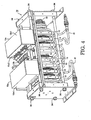
FIG. 4 is a perspective view of the semiconductor stack of the first embodiment; -
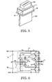
FIG. 5 is a perspective view of a neutral point bus-bar of the first embodiment; -
FIG. 6 is a circuit diagram showing current flows of a - U-phase circuit of the NPC inverter apparatus of the first embodiment;
-
FIG. 7 shows a wave form of a surge voltage that applies to a semiconductor switching device of the NPC inverter apparatus of the first embodiment; -
FIG. 8 shows a wave form of a transient ON voltage of a diode of the NPC inverter apparatus of the first embodiment; and -
FIG. 9 is a schematic front view of a semiconductor stack of an NPC inverter apparatus of a second embodiment. - The present invention is hereinafter described in detail by way of an illustrative embodiment.
- A three-level NPC inverter apparatus using IEGT of a first embodiment of the present invention is explained referring to
FIGs. 2-8 . - As shown in
FIG. 2 , a main circuit of the NPC inverter apparatus of the first embodiment includes a DC power source havingsmoothing capacitors capacitor 1a is connected between a positive electrode of the DC power source and a neutral point thereof. Thecapacitor 1b is connected between a negative electrode of the DC power source and the neutral point thereof. The respective U, V and W-phase circuits are connected to the DC power source and have the same formation each other. The U-phase circuit includessemiconductor switching devices diodes snubber circuits 12. Each of the semiconductor switching devices 6-9 includes an IEGT and a diode connected in anti-parallel to the IEGT. Therespective snubber circuits 12 are connected between the positive electrode and the neutral point, and the negative electrode and the neutral point respectively. Each of thesnubber circuits 12 includes asnubber capacitor 12a, asnubber diode 12b and adischarge resistor 12c. - A
semiconductor stack 18 mounting the above described main circuit is hereinafter described. - In general, the main circuit is refrigerated by an air-cooling or a water-cooling.
-
FIGs. 3 and4 show a water-cooling type of thesemiconductor stack 18 that includes the U-phase circuit inFIG. 2 .Cooling pipes 31 for the water cooling are shown inFIG. 4 . - As shown in
FIGs. 3 and4 , the first and second connectingdiodes bar 14C, are disposed in the middle of thesemiconductor stack 18. That is, the bus-bar 14C is connected to a neutral point of the first and second connectingdiodes FIG. 3 , the right side of the neutral point is a positive side of the DC power source, and the left side of the neutral point is a negative side of the DC power source. The first connectingdiode 10, aninsulating spacer 16, thesemiconductor switching devices fins 13 for refrigerating thesemiconductor switching devices semiconductor stack 18. Likewise, the second connectingdiode 11, aninsulating spacer 16, thesemiconductor switching devices cooling fins 13 for refrigerating thesemiconductor switching devices semiconductor stack 18. - The semiconductor switching devices 6-9, the connecting
diodes cooling fins 13, and theinsulating spacers 16 are stacked and pressured to each other at a predetermined pressure. - The
semiconductor stack 18 as constructed above is connected to the DC power source and thesnubber circuits 12. - Each case 12a1 of the
snubber capacitors 12a is made of brass or the like and forms terminal. The cases 12a1 are disposed adjacent to thesemiconductor stack 18 so that magnetic flux generated by current flowing in the case 12a1 (terminal) cancels magnetic flux caused by current flowing in thesemiconductor stack 18, and connected to thecooling fins 13 directly. Each of the other terminals of thesnubber capacitors 12a is divided into six terminals and includes an insulator 12a2 insulating from the case 12a1 as shown inFIG. 4 . The respective plural termainals are connected to terminals (an anode or a cathode) of thesnubber diodes 12b. The other terminals of thesnubber diodes 12b are the neutral point and are directly connected to acooling fin 17 for refrigerating thesnubber diodes 12b. That is, thecooling fin 17 is connected to the neutral point. - As shown in
FIG. 5 , the coolingfin 17 that functions to connect the terminals of thesnubber diodes 12b and to refrigerate thesnubber diodes 12b is secured to the neutral point bus-bar 14C forming a neutral point of the NPC inverter apparatus. As shown inFIGs. 3 and5 , the bus-bar 14C is fixed between an anode and a cathode of the connectingdiodes semiconductor stack 18 and formed in a shape of T. An area of a fixingplane 32 of the T-shaped bus-bar 14C is larger than an area of a fixingplane 33 of the coolingfin 17. - In the above description, although the bus-
bar 14C is formed in a shape of T, the bus-bar may be shaped in an inverse L. In this case, an anode and a cathode of the connectingdiodes plane 33 of the coolingfin 17, the same effect as the T-shaped bus-bar 14C may be achieved. - In the
semiconductor stack 18 of the first embodiment, electric modes of the NPC inverter apparatus that outputs a positive level, a neutral level and a negative level are explained referring toFIGs. 3 and6 . - A description of an output mode of the negative level is omitted, because a current direction of an output mode of the positive level is merely reversed.
- An arrow A in
FIG. 6 shows an output mode of the positive level of the U-phase circuit. - A current flows in a course of a positive bus-
bar 14P, thesemiconductor switching device 6, thesemiconductor switching device 7, and an output bus-bar 14U. As to thesemiconductor stack 18 having thesemiconductor switching devices FIG. 3 , a current flows in a course of the positive bus-bar 14P, the coolingfin 13, thesemiconductor switching device 6, the coolingfin 13, thesemiconductor switching device 7, the coolingfin 13, and the output bus-bar 14U as indicated by an arrow A inFIG. 3 . - Arrows B and C in
FIG. 6 show an output mode of the neutral level of the U-phase circuit. - A current flows in a course of the neutral point bus-
bar 14C, the connectingdiode 10, thesemiconductor switching device 7, the output bus-bar 14U, thesemiconductor switching device 8, the connectingdiode 11, and the neutral point bus-bar 14C. As to thesemiconductor stack 18 having the connectingdiode 10 and thesemiconductor switching device 7 shown inFIG. 3 , a current flows in a course of the bus-bar 14C, the connectingdiode 10, the coolingfin 13, a bus-bar 15P, the coolingfin 13, thesemiconductor switching device 7, the coolingfin 13, and the output bus-bar 14U as indicated by the arrow B inFIG. 3 , and further a current flows in a course of the output bus-bar 14U, the coolingfin 13, thesemiconductor switching device 8, the coolingfin 13, a bus-bar 15N, the coolingfin 13, the connectingdiode 11 and the neutral point bus-bar 14C. - The reason that a surge voltage is generated at the output modes is explained referring to
FIG. 7 . - Where a current IL flows in a condition that the
semiconductor switching devices semiconductor switching device 6 is made negative bias at a time t1 shown inFIG. 7 , thesemiconductor switching device 6 turns off, thereby increasing a voltage applying to thesemiconductor switching device 6 and reducing a current Ic flowing into thesemiconductor switching device 6. A surge voltage, which is caused by a rate of the current change (-dI/dt) and a wiring inductance of the main circuit of the NPC inverter apparatus, is applied to thesemiconductor switching device 6. A surge voltage Vs1 generated at a time t2 inFIG. 7 is represented by the followingformula 1. To restrain the surge voltage, it is needed to reduce the wiring inductance and to provide a diode that possesses a low transient ON voltage.
- A surge voltage Vs2 generated at a time t3 in
FIG. 7 is represented by the followingformula 2.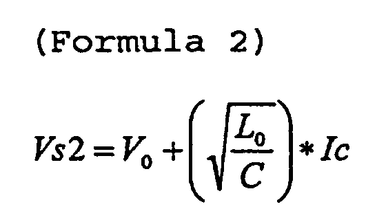
- V0 is a DC voltage. L0 is a wiring inductance from the smoothing
capacitor 1a to thesnubber circuit 12. L is the sum of wiring inductances of L1, L2, L3, L4 and L5. C is a capacity of the snubber capacity. Vfr is a transient ON voltage of thesnubber diode 12b. - According to the first embodiment, since each of the cases 12a1 of the
snubber capacitors 12a itself forms a terminal connected to the coolingfin 13 directly and the terminals of thesnubber capacitors 12a are disposed adjacent to thesemiconductor stack 18 so that magnetic flux generated by current flowing in the terminals cancels magnetic flux caused by current flowing in thesemiconductor stack 18, a wiring inductance of the NPC inverter apparatus may be minimized, thereby restraining a surge voltage that applies to the semiconductor switching devices 6-9. As a result, it is unnecessary to provide a snubber circuit to each of the semiconductor switching devices 6-9. - Further, wirings and components constituting the
snubber circuits 12 may be reduced in size. Furthermore, man-hours for assembly of the NPC inverter apparatus may be reduced. - In the above NPC inverter apparatus, the
snubber diode 12b possesses a low transient ON voltage. As shown inFIG.8 , a large voltage Vfr is generated at a time that a current with a large rate of current change (dI/dt) starts to flow into a diode, that is, while the electrons spread in all fields of a pellet of the diode. - As indicated in the
formula 1, the transient ON voltage Vfr of thesnubber diode 12b is a important factor for the surge voltage Vs1 that applies to thesemiconductor device 6. Therefore, a plurality ofsnubber diodes 12b that possess a low transient ON voltage are connected both in parallel and in serial. If the snubber diodes are connected in serial, a diode having a low voltage resistance may be used as a snubber diode. It is generally known that the diode having a low voltage resistance has a property of exceedingly low transient ON voltage. - If the snubber diodes are connected in parallel to each other, currents flowing in the snubber diodes are shared with the plural snubber diodes. Consequently, a transient ON voltage shown in
FIG. 8 is divided by the number of the snubber diodes. - Further, it is required to dispose the cooling
fins 13 for refrigerating the semiconductor switching devices 6-9, the connectingdiodes bars plates 16 are inserted between the coolingfins 13. - There are two ways to fix the insulating
plates 16. One is an adhesive fixation. Another is a screw fixation. As to the adhesive fixation, the strength of adhesive may become weak due to a cooling air. As to the screw fixation, since a screw is made of an insulator, the screw may become lose as years go by. Further, since holes are formed at screwed positions, reliability of electric non-conductance may be reduced. - To avoid the above problem, bridge types of the bus-
bars - According to the first embodiment, since a distance between the cooling
fins 13 and lengths of the bus-bars - Further, the semiconductor switching devices 6-9 and the cooling
fins 13 expand with heat generated by IEGT and the connectingdiodes FIG. 4 , thesemiconductor stack 18 is fastened withbolts 34 at a predetermined pressure. That is, the semiconductor switching devices 6-9, the connectingdiodes fins 13 are bound with thebolts 34. In case that a thermal stress caused by thermal expansion adds to an initial pressure of thesemiconductor stack 18, the total pressure maybe beyond a prescribed pressure of the semiconductor switching devices 6-9, whereby the semiconductor switching devices 6-9 may be broken. To avoid such situation, belleville springs 30 or plate springs (not shown) are placed on one end of thesemiconductor stack 18. - In such construction, if the bus-
bars bars - In order to obtain more spring effect, the bus-bar itself may be annealed, thereby reducing a bad influence caused by a thermal expansion.
- Even if an order of the components of the
semiconductor stack 18 changes, a wiring structure of thesnubber circuit 12 may be formed in the same way as the first embodiment. - An NPC inverter apparatus of a second embodiment of the present invention is explained referring to
FIG. 9 . - In the second embodiment, a cooling
fin 19 is substituted for the coolingfin 17 in the first embodiment. As shown inFIG. 9 , one terminal of thesnubber diode 12b is connected to the coolingfin 19 for refrigerating thesnebber diode 12b. The coolingfin 19 also refrigerates the connectingdiodes fin 19 also functions as an output terminal of a neutral point and includes a hole for connecting the neutral point bus-bar 14C. A depth of the coolingfin 19 is as wide as that of the coolingfin 13 in order to reduce a wiring inductance. - According to the second embodiment, since each of the cases 12a1 of the
snubber capacitors 12a itself forms a terminal connected to the coolingfin 13 directly and the terminals of thesnubber capacitors 12a are disposed adjacent to thesemiconductor stack 18 so that magnetic flux generated by current flowing in the terminals cancels magnetic flux caused by current flowing in thesemiconductor stack 18, a wiring inductance of the NPC inverter apparatus may be minimized, thereby restraining a surge voltage that applies to the semiconductor switching devices 6-9. As a result, it is unnecessary to provide a snubber circuit to each of the semiconductor switching devices 6-9. - According to the present invention, since a wiring inductance of the NPC inverter apparatus is minimized, a surge voltage may be restrained without attaching a snubber circuit to each of the semiconductor switching devices. That is, a surge voltage may be restrained by merely attaching a snubber circuit to a DC power source.
- Further, wirings and components constituting a snubber circuit may be reduced in size. Furthermore, man-hours for assembly of the NPC inverter apparatus may be reduced.
- Accordingly, since a surge voltage is restrained, it is possible to provide an economical and reliable power converter apparatus.
Claims (7)
- A power converter apparatus, comprising:a DC power source (Ed);a semiconductor stack (18), connected to said DC power source in parallel, having a plurality of semiconductor devices (6, 7, 8, 9) and a cooler (13, 31) for refrigerating said semiconductor devices, said semiconductor devices and said cooler are stacked and pressured to each other; anda snubber circuit (12), connected to said DC power source (Ed) in parallel, having a serial circuit of a capacitor (12a) and a diode (12b), and a resistor (12c) connected in parallel to said diode (12b), and characterized in that:one terminal of said capacitor (12a) is disposed adjacent to said semiconductor stack (18) so that magnetic flux generated by current flowing in said terminal cancels magnetic flux caused by current flowing in said semiconductor stack, and wherein said terminal of said capacitor (12a) is constituted by a case (12a1) of said capacitor.
- The power converter apparatus as recited in claim 1, wherein said case (12a1) is connected to said cooler (13, 31).
- The power converter apparatus as recited in claim 1, wherein the other terminal of said capacitor (12a) is divided into plural terminals.
- A power converter apparatus, comprising:a DC power source (Ed) having a positive electrode, a negative electrode and a neutral point;a semiconductor stack (18), connected to said DC power source in parallel, having a first cooler (13, 31) coupled to said positive electrode, a second cooler (13, 31) coupled to said negative electrode and a plurality of semiconductor devices (6, 7, 8, 9), said semiconductor devices and said first and second coolers are stacked and pressured to each other;a first snubber circuit (12), connected between said positive electrode and said neutral point, having a first serial circuit of a first capacitor (12a) and a first diode (12b), and a first resistor (12c) connected in parallel to said first diode (12b); anda second snubber circuit (12), connected between said negative electrode and said neutral point, having a second serial circuit of a second capacitor (12a) and a second diode (12b), and a second resistor (12c) connected in parallel to said second diode (12b), and characterized in that:one terminal of said first capacitor (12a) and one terminal of said second capacitor (12b) are disposed adjacent to said semiconductor stack (18) so that magnetic flux generated by current flowing in said terminals of said first and second capacitors (12a, 12b) cancels magnetic flux caused by current flowing in said semiconductor stack (18), and wherein said terminals of said first and second capacitors (12a, 12b) are constituted by cases (12a1) of said first and second capacitors respectively.
- The power converter apparatus as recited in claim 4, wherein said cases (12a1) of said first and second capacitors (12a, 12b) are connected to said first and second coolers (13, 31) respectively.
- The power converter apparatus as recited in claim 4, further comprising:a third cooler (17) coupled to said neutral point, one terminal on said first diode (12a) side of said first serial circuit and one terminal on said second diode (12b) side of said second serial circuit are connected to said third cooler (17).
- The power converter apparatus as recited in claim 6, further comprising:a bus-bar (14c), connected to said neutral point, for functioning as an electrode of said semiconductor devices and fixing said third cooler (17) on a fixing plane (32) thereof,an area of said fixing plane (32) is equal to or larger than an area of a fixing plane (33) of said third cooler (17).
Applications Claiming Priority (2)
| Application Number | Priority Date | Filing Date | Title |
|---|---|---|---|
| JP25105199A JP3652934B2 (en) | 1999-09-06 | 1999-09-06 | Power converter |
| JP25105199 | 1999-09-06 |
Publications (2)
| Publication Number | Publication Date |
|---|---|
| EP1081833A1 EP1081833A1 (en) | 2001-03-07 |
| EP1081833B1 true EP1081833B1 (en) | 2010-03-17 |
Family
ID=17216898
Family Applications (1)
| Application Number | Title | Priority Date | Filing Date |
|---|---|---|---|
| EP00119313A Expired - Lifetime EP1081833B1 (en) | 1999-09-06 | 2000-09-06 | Power converter apparatus |
Country Status (6)
| Country | Link |
|---|---|
| US (1) | US6272028B1 (en) |
| EP (1) | EP1081833B1 (en) |
| JP (1) | JP3652934B2 (en) |
| CN (1) | CN1197232C (en) |
| CA (1) | CA2317350C (en) |
| DE (1) | DE60044009D1 (en) |
Families Citing this family (23)
| Publication number | Priority date | Publication date | Assignee | Title |
|---|---|---|---|---|
| GB2360883B (en) * | 2000-03-31 | 2004-04-21 | Nordson Corp | Inverter circuit |
| JP3665934B2 (en) * | 2001-08-03 | 2005-06-29 | 株式会社日立製作所 | 3-level inverter device |
| JP2003079162A (en) * | 2001-09-03 | 2003-03-14 | Toshiba Transport Eng Inc | Power converter |
| JP4664104B2 (en) * | 2005-03-24 | 2011-04-06 | 東芝三菱電機産業システム株式会社 | Power converter |
| JP4600159B2 (en) * | 2005-06-01 | 2010-12-15 | 三菱電機株式会社 | 3-level power converter |
| JP5169092B2 (en) * | 2007-09-11 | 2013-03-27 | 株式会社デンソー | Power converter |
| EP2302772A1 (en) * | 2009-09-28 | 2011-03-30 | ABB Oy | Inverter |
| FR2962608B1 (en) * | 2010-07-07 | 2012-08-10 | Toulouse Inst Nat Polytech | NEW REDUNDANCY STRUCTURES FOR STATIC CONVERTERS |
| DE102010038511A1 (en) * | 2010-07-28 | 2012-02-02 | Robert Bosch Gmbh | Overvoltage protection circuit for at least one branch of a half-bridge, inverter, DC-DC converter and circuit arrangement for operating an electrical machine |
| JP5999677B2 (en) * | 2011-09-20 | 2016-09-28 | ローム株式会社 | Electronic circuit |
| JP5663450B2 (en) * | 2011-10-18 | 2015-02-04 | 株式会社日立製作所 | Power converter |
| JP5655846B2 (en) * | 2012-12-04 | 2015-01-21 | 株式会社デンソー | Power converter |
| DE202013104510U1 (en) * | 2013-10-04 | 2013-11-14 | Abb Technology Ag | Semiconductor stack for converters with snubber capacitors |
| CN104953857A (en) * | 2015-06-18 | 2015-09-30 | 国电南瑞科技股份有限公司 | Power unit of IEGT (Injection Enhanced Gate Transistor)-based high-power tri-level converter |
| US10850623B2 (en) * | 2017-10-30 | 2020-12-01 | Sf Motors, Inc. | Stacked electric vehicle inverter cells |
| US10790758B2 (en) | 2018-03-08 | 2020-09-29 | Chongqing Jinkang New Energy Vehicle Co., Ltd. | Power converter for electric vehicle drive systems |
| US10779445B2 (en) | 2018-03-23 | 2020-09-15 | Chongqing Jinkang New Energy Vehicle Co., Ltd. | Inverter module having multiple half-bridge modules for a power converter of an electric vehicle |
| US10594230B2 (en) | 2018-03-23 | 2020-03-17 | Sf Motors, Inc. | Inverter module having multiple half-bridge modules for a power converter of an electric vehicle |
| US10778117B2 (en) | 2018-04-17 | 2020-09-15 | Chongqing Jinkang New Energy Vehicle Co., Ltd. | Inverter module of an electric vehicle |
| US10772242B2 (en) | 2018-04-17 | 2020-09-08 | Chongqing Jinkang New Energy Vehicle Co., Ltd. | Inverter module of an electric vehicle |
| US10660242B2 (en) | 2018-04-26 | 2020-05-19 | Chongqing Jinkang New Energy Vehicle Co., Ltd. | Electric vehicle inverter module heat sink |
| JP7276006B2 (en) * | 2019-08-29 | 2023-05-18 | 富士電機株式会社 | Snubber circuit and power converter |
| DE102019218953A1 (en) * | 2019-12-05 | 2021-06-10 | Robert Bosch Gmbh | Electronic circuit unit |
Family Cites Families (10)
| Publication number | Priority date | Publication date | Assignee | Title |
|---|---|---|---|---|
| JPS5866575A (en) * | 1981-10-13 | 1983-04-20 | Mitsubishi Electric Corp | Semiconductor device |
| JPH04322174A (en) * | 1991-04-19 | 1992-11-12 | Toshiba Corp | Power converting apparatus for vehicle |
| JPH05227764A (en) * | 1992-02-10 | 1993-09-03 | Toshiba Corp | Inverter |
| JPH0756629A (en) | 1993-08-18 | 1995-03-03 | Daifuku Co Ltd | Mobile vehicle guidance equipment |
| JP3153408B2 (en) * | 1994-03-10 | 2001-04-09 | 株式会社日立製作所 | Series multiplex power converter |
| JPH0869893A (en) | 1994-08-30 | 1996-03-12 | Hitachi Medical Corp | Inverter type x-ray device |
| JPH09285136A (en) | 1996-04-19 | 1997-10-31 | Toshiba Corp | Power converter |
| CA2261616C (en) * | 1996-07-22 | 2004-11-09 | Hydro-Quebec | Low stray interconnection inductance power converting module for converting a dc voltage into an ac voltage, and a method therefor |
| JPH1094256A (en) * | 1996-09-19 | 1998-04-10 | Toshiba Corp | Power conversion element module |
| JP3229931B2 (en) | 1997-09-08 | 2001-11-19 | 三菱電機株式会社 | 3-level power converter |
-
1999
- 1999-09-06 JP JP25105199A patent/JP3652934B2/en not_active Expired - Lifetime
-
2000
- 2000-08-28 US US09/649,001 patent/US6272028B1/en not_active Expired - Lifetime
- 2000-09-05 CA CA002317350A patent/CA2317350C/en not_active Expired - Lifetime
- 2000-09-06 EP EP00119313A patent/EP1081833B1/en not_active Expired - Lifetime
- 2000-09-06 DE DE60044009T patent/DE60044009D1/en not_active Expired - Lifetime
- 2000-09-06 CN CN00126368.4A patent/CN1197232C/en not_active Expired - Lifetime
Also Published As
| Publication number | Publication date |
|---|---|
| US6272028B1 (en) | 2001-08-07 |
| EP1081833A1 (en) | 2001-03-07 |
| JP2001078467A (en) | 2001-03-23 |
| DE60044009D1 (en) | 2010-04-29 |
| CN1197232C (en) | 2005-04-13 |
| CN1287404A (en) | 2001-03-14 |
| CA2317350A1 (en) | 2001-03-06 |
| CA2317350C (en) | 2008-02-12 |
| JP3652934B2 (en) | 2005-05-25 |
Similar Documents
| Publication | Publication Date | Title |
|---|---|---|
| US6272028B1 (en) | Power converter apparatus | |
| US5132896A (en) | Inverter unit with improved bus-plate configuration | |
| US10134718B2 (en) | Power semiconductor module | |
| US20160345463A1 (en) | Cooling Structure of Heating Element and Power Conversion Device | |
| JP6836201B2 (en) | Power converter | |
| JPWO2007113979A1 (en) | Power conversion device and assembly method thereof | |
| JPH088397A (en) | Low inductance power semiconductor module | |
| US10164519B2 (en) | Semiconductor stack for converter with snubber capacitors | |
| US10554123B2 (en) | Power converter with a parallel flat plate conductor electrically connected with a capacitor and a power module | |
| US20170117820A1 (en) | Semiconductor device | |
| US6795324B2 (en) | Power converter | |
| EP1010234A1 (en) | High power inverter pole employing series connected devices configured for reduced stray loop inductance | |
| JP2021035205A (en) | Semiconductor switching unit | |
| JP7364103B2 (en) | power converter | |
| JP4664104B2 (en) | Power converter | |
| Boutry | Theoretical and experimental evaluation of the Integrated gate-commutated thyristor (IGCT) as a switch for Modular Multi Level Converters (MMC) | |
| JP3390679B2 (en) | Inverter device | |
| EP3026802A1 (en) | Power module | |
| RU2190919C2 (en) | Power circuit of electric power inverter | |
| JP4154671B2 (en) | Power semiconductor module | |
| CN223231056U (en) | Power module and power conversion device with same | |
| EP4668582A1 (en) | A power conversion device for an electrical car | |
| US12301215B2 (en) | Fast electronic switch | |
| JP2024101333A (en) | Power Conversion Equipment | |
| EP4651378A1 (en) | Switch stacking circuit and switch stacking device comprising same |
Legal Events
| Date | Code | Title | Description |
|---|---|---|---|
| PUAI | Public reference made under article 153(3) epc to a published international application that has entered the european phase |
Free format text: ORIGINAL CODE: 0009012 |
|
| 17P | Request for examination filed |
Effective date: 20000906 |
|
| AK | Designated contracting states |
Kind code of ref document: A1 Designated state(s): CH DE LI |
|
| AX | Request for extension of the european patent |
Free format text: AL;LT;LV;MK;RO;SI |
|
| AKX | Designation fees paid |
Free format text: CH DE LI |
|
| 17Q | First examination report despatched |
Effective date: 20080606 |
|
| GRAP | Despatch of communication of intention to grant a patent |
Free format text: ORIGINAL CODE: EPIDOSNIGR1 |
|
| GRAS | Grant fee paid |
Free format text: ORIGINAL CODE: EPIDOSNIGR3 |
|
| GRAA | (expected) grant |
Free format text: ORIGINAL CODE: 0009210 |
|
| AK | Designated contracting states |
Kind code of ref document: B1 Designated state(s): CH DE LI |
|
| REG | Reference to a national code |
Ref country code: CH Ref legal event code: NV Representative=s name: E. BLUM & CO. AG PATENT- UND MARKENANWAELTE VSP Ref country code: CH Ref legal event code: EP |
|
| REF | Corresponds to: |
Ref document number: 60044009 Country of ref document: DE Date of ref document: 20100429 Kind code of ref document: P |
|
| RAP2 | Party data changed (patent owner data changed or rights of a patent transferred) |
Owner name: TOSHIBA MITSUBISHI-ELECTRIC INDUSTRIAL SYSTEMS COR |
|
| RAP2 | Party data changed (patent owner data changed or rights of a patent transferred) |
Owner name: TOSHIBA MITSUBISHI-ELECTRIC INDUSTRIAL SYSTEMS COR |
|
| REG | Reference to a national code |
Ref country code: CH Ref legal event code: PUE Owner name: TOSHIBA MITSUBISHI-ELECTRIC INDUSTRIAL SYSTEMS CO Free format text: KABUSHIKI KAISHA TOSHIBA#72, HORIKAWA-CHO, SAIWAI-KU#KAWASAKI-SHI, KANAGAWA-KEN 210-8572 (JP) -TRANSFER TO- TOSHIBA MITSUBISHI-ELECTRIC INDUSTRIAL SYSTEMS CORPORATION#13-16, MITA 3-CHOME MINATO-KU,#TOKYO 108-0073 (JP) |
|
| PLBE | No opposition filed within time limit |
Free format text: ORIGINAL CODE: 0009261 |
|
| STAA | Information on the status of an ep patent application or granted ep patent |
Free format text: STATUS: NO OPPOSITION FILED WITHIN TIME LIMIT |
|
| 26N | No opposition filed |
Effective date: 20101220 |
|
| REG | Reference to a national code |
Ref country code: DE Ref legal event code: R081 Ref document number: 60044009 Country of ref document: DE Owner name: TOSHIBA MITSUBISHI-ELECTRIC INDUSTRIAL SYSTEMS, JP Free format text: FORMER OWNER: KABUSHIKI KAISHA TOSHIBA, KAWASAKI, KANAGAWA, JP Effective date: 20110429 |
|
| PGFP | Annual fee paid to national office [announced via postgrant information from national office to epo] |
Ref country code: DE Payment date: 20190827 Year of fee payment: 20 |
|
| PGFP | Annual fee paid to national office [announced via postgrant information from national office to epo] |
Ref country code: CH Payment date: 20190913 Year of fee payment: 20 |
|
| REG | Reference to a national code |
Ref country code: DE Ref legal event code: R071 Ref document number: 60044009 Country of ref document: DE |
|
| REG | Reference to a national code |
Ref country code: CH Ref legal event code: PL |