EP1080925A1 - Method of manufacturing thermal head - Google Patents
Method of manufacturing thermal head Download PDFInfo
- Publication number
- EP1080925A1 EP1080925A1 EP00908043A EP00908043A EP1080925A1 EP 1080925 A1 EP1080925 A1 EP 1080925A1 EP 00908043 A EP00908043 A EP 00908043A EP 00908043 A EP00908043 A EP 00908043A EP 1080925 A1 EP1080925 A1 EP 1080925A1
- Authority
- EP
- European Patent Office
- Prior art keywords
- protective film
- wiring electrode
- unnecessary
- thermal head
- heater resistor
- Prior art date
- Legal status (The legal status is an assumption and is not a legal conclusion. Google has not performed a legal analysis and makes no representation as to the accuracy of the status listed.)
- Granted
Links
Images

Classifications
-
- B—PERFORMING OPERATIONS; TRANSPORTING
- B41—PRINTING; LINING MACHINES; TYPEWRITERS; STAMPS
- B41J—TYPEWRITERS; SELECTIVE PRINTING MECHANISMS, i.e. MECHANISMS PRINTING OTHERWISE THAN FROM A FORME; CORRECTION OF TYPOGRAPHICAL ERRORS
- B41J2/00—Typewriters or selective printing mechanisms characterised by the printing or marking process for which they are designed
- B41J2/315—Typewriters or selective printing mechanisms characterised by the printing or marking process for which they are designed characterised by selective application of heat to a heat sensitive printing or impression-transfer material
- B41J2/32—Typewriters or selective printing mechanisms characterised by the printing or marking process for which they are designed characterised by selective application of heat to a heat sensitive printing or impression-transfer material using thermal heads
- B41J2/335—Structure of thermal heads
- B41J2/33505—Constructional details
- B41J2/3353—Protective layers
-
- B—PERFORMING OPERATIONS; TRANSPORTING
- B41—PRINTING; LINING MACHINES; TYPEWRITERS; STAMPS
- B41J—TYPEWRITERS; SELECTIVE PRINTING MECHANISMS, i.e. MECHANISMS PRINTING OTHERWISE THAN FROM A FORME; CORRECTION OF TYPOGRAPHICAL ERRORS
- B41J2/00—Typewriters or selective printing mechanisms characterised by the printing or marking process for which they are designed
- B41J2/315—Typewriters or selective printing mechanisms characterised by the printing or marking process for which they are designed characterised by selective application of heat to a heat sensitive printing or impression-transfer material
- B41J2/32—Typewriters or selective printing mechanisms characterised by the printing or marking process for which they are designed characterised by selective application of heat to a heat sensitive printing or impression-transfer material using thermal heads
- B41J2/335—Structure of thermal heads
- B41J2/3355—Structure of thermal heads characterised by materials
-
- B—PERFORMING OPERATIONS; TRANSPORTING
- B41—PRINTING; LINING MACHINES; TYPEWRITERS; STAMPS
- B41J—TYPEWRITERS; SELECTIVE PRINTING MECHANISMS, i.e. MECHANISMS PRINTING OTHERWISE THAN FROM A FORME; CORRECTION OF TYPOGRAPHICAL ERRORS
- B41J2/00—Typewriters or selective printing mechanisms characterised by the printing or marking process for which they are designed
- B41J2/315—Typewriters or selective printing mechanisms characterised by the printing or marking process for which they are designed characterised by selective application of heat to a heat sensitive printing or impression-transfer material
- B41J2/32—Typewriters or selective printing mechanisms characterised by the printing or marking process for which they are designed characterised by selective application of heat to a heat sensitive printing or impression-transfer material using thermal heads
- B41J2/335—Structure of thermal heads
- B41J2/33555—Structure of thermal heads characterised by type
- B41J2/3357—Surface type resistors
-
- B—PERFORMING OPERATIONS; TRANSPORTING
- B41—PRINTING; LINING MACHINES; TYPEWRITERS; STAMPS
- B41J—TYPEWRITERS; SELECTIVE PRINTING MECHANISMS, i.e. MECHANISMS PRINTING OTHERWISE THAN FROM A FORME; CORRECTION OF TYPOGRAPHICAL ERRORS
- B41J2/00—Typewriters or selective printing mechanisms characterised by the printing or marking process for which they are designed
- B41J2/315—Typewriters or selective printing mechanisms characterised by the printing or marking process for which they are designed characterised by selective application of heat to a heat sensitive printing or impression-transfer material
- B41J2/32—Typewriters or selective printing mechanisms characterised by the printing or marking process for which they are designed characterised by selective application of heat to a heat sensitive printing or impression-transfer material using thermal heads
- B41J2/335—Structure of thermal heads
- B41J2/3359—Manufacturing processes
-
- Y—GENERAL TAGGING OF NEW TECHNOLOGICAL DEVELOPMENTS; GENERAL TAGGING OF CROSS-SECTIONAL TECHNOLOGIES SPANNING OVER SEVERAL SECTIONS OF THE IPC; TECHNICAL SUBJECTS COVERED BY FORMER USPC CROSS-REFERENCE ART COLLECTIONS [XRACs] AND DIGESTS
- Y10—TECHNICAL SUBJECTS COVERED BY FORMER USPC
- Y10T—TECHNICAL SUBJECTS COVERED BY FORMER US CLASSIFICATION
- Y10T29/00—Metal working
- Y10T29/49—Method of mechanical manufacture
- Y10T29/49002—Electrical device making
- Y10T29/49082—Resistor making
- Y10T29/49083—Heater type
-
- Y—GENERAL TAGGING OF NEW TECHNOLOGICAL DEVELOPMENTS; GENERAL TAGGING OF CROSS-SECTIONAL TECHNOLOGIES SPANNING OVER SEVERAL SECTIONS OF THE IPC; TECHNICAL SUBJECTS COVERED BY FORMER USPC CROSS-REFERENCE ART COLLECTIONS [XRACs] AND DIGESTS
- Y10—TECHNICAL SUBJECTS COVERED BY FORMER USPC
- Y10T—TECHNICAL SUBJECTS COVERED BY FORMER US CLASSIFICATION
- Y10T29/00—Metal working
- Y10T29/49—Method of mechanical manufacture
- Y10T29/49002—Electrical device making
- Y10T29/49082—Resistor making
- Y10T29/49101—Applying terminal
-
- Y—GENERAL TAGGING OF NEW TECHNOLOGICAL DEVELOPMENTS; GENERAL TAGGING OF CROSS-SECTIONAL TECHNOLOGIES SPANNING OVER SEVERAL SECTIONS OF THE IPC; TECHNICAL SUBJECTS COVERED BY FORMER USPC CROSS-REFERENCE ART COLLECTIONS [XRACs] AND DIGESTS
- Y10—TECHNICAL SUBJECTS COVERED BY FORMER USPC
- Y10T—TECHNICAL SUBJECTS COVERED BY FORMER US CLASSIFICATION
- Y10T29/00—Metal working
- Y10T29/49—Method of mechanical manufacture
- Y10T29/49789—Obtaining plural product pieces from unitary workpiece
-
- Y—GENERAL TAGGING OF NEW TECHNOLOGICAL DEVELOPMENTS; GENERAL TAGGING OF CROSS-SECTIONAL TECHNOLOGIES SPANNING OVER SEVERAL SECTIONS OF THE IPC; TECHNICAL SUBJECTS COVERED BY FORMER USPC CROSS-REFERENCE ART COLLECTIONS [XRACs] AND DIGESTS
- Y10—TECHNICAL SUBJECTS COVERED BY FORMER USPC
- Y10T—TECHNICAL SUBJECTS COVERED BY FORMER US CLASSIFICATION
- Y10T29/00—Metal working
- Y10T29/49—Method of mechanical manufacture
- Y10T29/49789—Obtaining plural product pieces from unitary workpiece
- Y10T29/4979—Breaking through weakened portion
Definitions
- the present invention relates to a method of manufacturing a thermal head for use in thermal recording in a facsimile machine, a printer, or the like.
- a glaze layer 2 as a heat storage layer is provided on an insulating substrate 1 such as a ceramic substrate, a heater resistor material of a Ta system, a sulicide system, an Ni-Cr system, or the like and an electrode material of Al, Cr-Cu, Au, or the like are formed by sputtering, deposition, or the like, a heater resistor 3, a common electrode, and a wiring electrode 4 for an individual electrode are formed by patterning in a photolithographic process, and, after that, a protective film 6 of SiO2, Ta2O5, SiAlON, Si3N4, Sic, or the like for inhibiting oxidation and for resisting wear of the heater resistor 3 is formed by sputtering, ion plating, or CVD to manufacture a thermal head.
- the protective film 6 has to be selectively formed in the heater resistor portion for the purpose of inhibiting oxidation and resisting wear, such that the protective film 6 does not remain at a portion 4a where the protective film is unnecessary such as a wire bonding portion to a driver IC for sending an image signal through the electrode to a heater resistor and the like.
- Several ways are conventionally known for selectively forming the protective film 6.
- Fig. 2(a) there is a way where physical masking is carried out.
- a metal mask 7 masks the substrate.
- the protective film 6 wraps around to the space between the metal mask 7 and the substrate, a protective film wraparound portion 6a is formed, and the protective film 6 remains even at the portion 4a where the protective film is unnecessary.
- the protective film wraparound portion 6a is designed so as to be admitted, which is a factor that inhibits miniaturization of the substrate size, increase in the number of the thermal heads taken from one substrate, and the like.
- Another way is to imbricate substrates.
- the wiring electrode 4 is damaged by contact.
- a space has to be provided between the substrates, which causes a disadvantage that the protective film 6 remains even at the portion 4a where the protective film is unnecessary.
- a wafer-like substrate has to be cut into long substrates. Cutting and imbricating the substrates takes time, causes increase in steps of the production process, and is a factor that increases the cost.
- the substrates have to go through the production process in the cut state even at steps subsequent to the formation of the protective film 6, there is a disadvantage that the production touring is deteriorated.
- the protective film 6 is chemically etched to selectively form the protective film 6.
- an inorganic ceramic film is used which is chemically and physically stable. Therefore, it is etched using a chemical of a hydrogen fluoride system.
- a chemical has an extremely slow etching rate, which is a factor that lowers the productivity. This is true of not only etching using a chemical but also dry etching using a vapor phase method.
- etching using a chemical has a disadvantage that, since a metal is used as the wiring electrode 4, the etching selectivity to the protective film 6 can not be secured and even the wiring electrode 4 is etched. Therefore, this is not practical in the field of thermal heads.
- the protective film is formed at a high temperature in a high vacuum.
- the photoresist is exposed to the high temperature and the high vacuum. Since the photoresist is a resin, it can not withstand the conditions when the protective film is formed, and generates gas in a vacuum container. Such gas not only contaminates the inside of the vacuum container but also deteriorates the adhesion and the quality of the protective film, which may be a factor that decreases the reliability of the thermal head.
- the masking agent is peeled off, since the resin is carbonized, i.e., burned out, it can not be peeled off, the masking agent remains on the wiring electrode at the portion where the protective film is unnecessary, wire bonding for connecting a driver IC for sending an image signal through the electrode to the heater resistor and the like can not be carried out, and the essential function of the thermal head is not carried out.
- a masking agent of a polyimide system which is more heat-resistant than such photoresist is also used.
- polyimide is heat-resistant, once it is cured, its peelability deteriorates extremely. At that time, although the amount is small the masking agent remains on the wiring electrode. If the masking agent remains, it becomes a factor that decreases the reliability in mounting and the productivity. For example, since the strength of the wire bonding for connection to a driver IC for sending an image signal through the electrode to the heater resistor and the like can not be secured, the wire bonding may be detached. To compulsorily peel it off, a polar solvent such as NMP for dissolving the polyimide has to be used. The use of such a polar solvent adversely affects the operator and the working environment. In addition, there is a problem that, since the consciousness of protecting the global environment has been raised recently, a strong chemical can not be used unconditionally.
- an object of the present invention is, in order to solve the conventional problems mentioned in the above, to obtain a method of manufacturing a thermal head which can, by using inorganic paste as the masking agent, accommodate miniaturization of the substrate and an increased number of the thermal heads taken from one substrate, and which can selectively form a protective film with high positioning accuracy of the protective film, with high adhesion of the protective film, and with high reliability.
- a thermal head having on an insulating substrate at least a heater resistor, a wiring electrode for supplying electric power to the heater resistor, and a protective film for covering the heater and the wiring electrode on the periphery thereof
- at least the heater resistor and the wiring electrode for supplying electric power to the heater resistor are formed on the insulating substrate, a portion where the protective film is unnecessary of the wiring electrode where a driver IC for sending an image signal through the electrode to the heater resistor and the thermal head are connected by wire bonding is masked using inorganic paste, the protective film is formed over the whole surface, and then, the protective film of the portion where the protective film is unnecessary is peeled oft together with the inorganic paste to selectively form the protective film on the heater and a heat generating portion of the wiring electrode on the periphery thereof.
- a thermal head constituted as in the above, since the portion where the protective film is unnecessary is masked using the inorganic paste and the masking agent for forming the protective film contains no resin therein, the heat resistance is extremely high, and gas is not generated in a vacuum container at a high temperature in a high vacuum. Therefore, the inside of the vacuum container is not contaminated, and high adhesion of the film and high reliability of the film can be obtained.
- its heat resistance is extremely high and it contains no resin component, there is no phenomenon such as carbonization and burnout, which facilitates its peeling off. Therefore, the masking agent does not remain on the wiring electrode, and thus, the strength of the wire bonding is improved.
- the masking agent can be used at an arbitrary position, the protective film can be formed selectively, and thus, the substrate size can be made smaller, the number of the thermal heads taken from one substrate increases, and the productivity is improved.
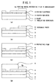
- Fig. 1 is a figure illustrating the process of a method of manufacturing a thermal head according to the present invention.
- the process of the manufacturing method of the present application is described in due order.
- a glaze 2 is formed for heat storage on an insulating substrate 1 made of alumina ceramics or the like.
- a film as a heater resistor material of Ta-N, Ta-SiO2, or the like the main component of which is Ta is formed by sputtering at the thickness of about 0.1 ⁇ m.
- a heater resistor 3 is formed by photolithography.
- a film as an electrode material for supplying electric power to the heater resistor 3 of Al, Al-Si, Al-Si-Cu, or the like the main component of which is Al is formed by sputtering or the like at the thickness of about 1 - 2 ⁇ m.
- a wiring electrode 4 is formed by photolithography.
- the wiring electrode 4 is provided with a portion 4a where a protective film is unnecessary, which is for later connection to a driver IC for sending an image signal through the electrode to the heater resistor or the like by wire bonding or the like.
- inorganic paste 5 is formed of pure water, ceramic powder the main component of which is alumina, silica, or the like, and bentonite as a binding component. They are mixed into paste, and used as the inorganic paste 5.
- the particle size of the ceramic powder used here is about 1 - 5 ⁇ m. If the particle size of the ceramic powder is larger than 5 ⁇ m, inconvenience such as lowered printability is sometimes caused, and thus, it is not practical.
- Bentonite as the binding component is a layered silicate containing moisture the main component of which is montmorillonite which is a clay mineral, and has characteristics to be swelled by water and increase the viscosity. Therefore, it is most suitable for making an inorganic matter into paste for printing. In addition, since no organic matter is contained, the heat resistance is excellent and no gas is generated even at a high temperature in a high vacuum.
- the mixed inorganic paste 5 is applied to the portion 4a where the protective film is unnecessary of the wiring electrode 4.
- screen printing is most suitable. Since screen printing has high productivity and high printing accuracy, and can form various patterns by changing the shape of the screen mask, it is effective in selectively applying the inorganic paste 5 to the portion 4a where the protective film is unnecessary of the wiring electrode 4.
- the inorganic paste 5 is printed at the thickness of about 10 - 30 ⁇ m by screen printing. Since the film thickness to be printed depends on the film thickness of a protective film 6 to be formed later, it is required to be at least twice as thick as the film thickness of the protective film 6. If the film thickness is equivalent to or is smaller than the film thickness of the protective film, the peelability which is necessary in a subsequent step deteriorates.
- applying methods include application using a dispenser or the like, offset printing using a roller, and flexography.
- the applying method can be selected so as to match the shape into which the paste is applied.
- the inorganic paste 5 After that, by drying the inorganic paste 5 at 150 °C or higher, moisture in it evaporates. Evaporation of moisture makes the inorganic paste 5 cure to mask the portion 4a where the protective film is unnecessary of the wiring electrode 4.
- a film which is a mixture of Si3N4 and SiO2 or the like is formed by sputtering or the like at the thickness of about 3 - 6 ⁇ m over the whole surface of the substrate so as to cover all of the heater resistor 3, the wiring electrode 4, and the inorganic paste 5, and the protective film 6 is formed over the whole surface.
- the substrate with the protective film 6 formed over the whole surface thereof is soaked in water such as pure water.
- water such as pure water.
- ultrasonic cleaning is effective.
- a low frequency band such as 28 - 45 kHz is effective.
- cleaning using a high frequency band of 100 kHz or higher is more effective.
- a way of running water cleaning with pressurized water such as waterjet or the like is also effective.
- the protective film 6 at the portion 4a where the protective film is unnecessary is removed, and the protective film 6 is selectively formed on the heater resistor 3 and a heat generating portion of the wiring electrode 4 on the periphery thereof.
- the protective film of a thermal head is selectively formed using inorganic paste, the substrate size is made smaller, the number of the thermal heads taken from one substrate increases, and the productivity is improved. Further, since selective formation can be carried out, a complicated protective film having a through hole or a multilayer wiring electrode constitution can be formed, which improves the degree of freedom in designing a thermal head.
Landscapes
- Engineering & Computer Science (AREA)
- Manufacturing & Machinery (AREA)
- Electronic Switches (AREA)
Abstract
In order to attain this, a portion where the protective film is unnecessary of a wiring electrode is masked using inorganic paste, the protective film is formed over the whole surface, and then, the protective film at the portion where the protective film is unnecessary is peeled off together with the inorganic paste to selectively form the protective film on a heater and a heat generating portion of the wiring electrode on the periphery thereof.
Description
at least the heater resistor and the wiring electrode for supplying electric power to the heater resistor are formed on the insulating substrate, a portion where the protective film is unnecessary of the wiring electrode where a driver IC for sending an image signal through the electrode to the heater resistor and the thermal head are connected by wire bonding is masked using inorganic paste, the protective film is formed over the whole surface, and then, the protective film of the portion where the protective film is unnecessary is peeled oft together with the inorganic paste to selectively form the protective film on the heater and a heat generating portion of the wiring electrode on the periphery thereof.
Fig. 1 is a figure illustrating the process of a method of manufacturing a thermal head according to the present invention. The process of the manufacturing method of the present application is described in due order. As shown in Fig. 1(a), a
Claims (3)
- A method of manufacturing a thermal head having on an insulating substrate at least a heater resistor, a wiring electrode for supplying electric power to the heater resistor, and a protective film for covering the heater and the wiring electrode on the periphery thereof, characterized in that:at least the heater resistor and the wiring electrode for supplying electric power to the heater resistor are formed on the insulating substrate, a portion where said protective film is unnecessary of the wiring electrode where a driver IC for sending an image signal through said electrode to said heater resistor and said thermal head are connected by wire bonding is masked using inorganic paste, said protective film is formed over the whole surface, and then, said protective film at said portion where said protective film is unnecessary is peeled off together with said inorganic paste to selectively form said protective film on the heater and a heat generating portion of the wiring electrode on the periphery thereof.
- A method of manufacturing a thermal head as claimed in claim 1, wherein the main component of said inorganic paste for masking said portion where said protective film is unnecessary is ceramic powder of alumina, silica, or the like.
- A method of manufacturing a thermal head as claimed in claim 1, wherein a binding component of said inorganic paste for masking said portion where said protective film is unnecessary is bentonite that is a layered silicate containing moisture the main component of which is montmorillonite which is a clay mineral and the like.
Applications Claiming Priority (3)
| Application Number | Priority Date | Filing Date | Title |
|---|---|---|---|
| JP7598999 | 1999-03-19 | ||
| JP7598999 | 1999-03-19 | ||
| PCT/JP2000/001517 WO2000056550A1 (en) | 1999-03-19 | 2000-03-13 | Method of manufacturing thermal head |
Publications (3)
| Publication Number | Publication Date |
|---|---|
| EP1080925A1 true EP1080925A1 (en) | 2001-03-07 |
| EP1080925A4 EP1080925A4 (en) | 2002-05-29 |
| EP1080925B1 EP1080925B1 (en) | 2003-07-30 |
Family
ID=13592202
Family Applications (1)
| Application Number | Title | Priority Date | Filing Date |
|---|---|---|---|
| EP00908043A Expired - Lifetime EP1080925B1 (en) | 1999-03-19 | 2000-03-13 | Method of manufacturing thermal head |
Country Status (6)
| Country | Link |
|---|---|
| US (1) | US6560855B1 (en) |
| EP (1) | EP1080925B1 (en) |
| JP (1) | JP3989684B2 (en) |
| KR (1) | KR20010025016A (en) |
| DE (1) | DE60004143T2 (en) |
| WO (1) | WO2000056550A1 (en) |
Families Citing this family (7)
| Publication number | Priority date | Publication date | Assignee | Title |
|---|---|---|---|---|
| JP2004319881A (en) * | 2003-04-18 | 2004-11-11 | Alps Electric Co Ltd | Wiring substrate and electric apparatus and switch comprising it |
| JP4619102B2 (en) * | 2004-10-27 | 2011-01-26 | 京セラ株式会社 | Thermal head and thermal printer |
| JP2009137284A (en) * | 2007-11-13 | 2009-06-25 | Tdk Corp | Thermal head, manufacturing method for thermal head, and printer |
| JP5401782B2 (en) * | 2007-11-30 | 2014-01-29 | 株式会社豊田中央研究所 | Thermal storage device and manufacturing method thereof |
| JP5223314B2 (en) * | 2007-11-30 | 2013-06-26 | 株式会社豊田中央研究所 | Heat storage device |
| US8861317B1 (en) | 2013-04-02 | 2014-10-14 | Western Digital (Fremont), Llc | Heat assisted magnetic recording transducer having protective pads |
| US9343098B1 (en) | 2013-08-23 | 2016-05-17 | Western Digital (Fremont), Llc | Method for providing a heat assisted magnetic recording transducer having protective pads |
Family Cites Families (13)
| Publication number | Priority date | Publication date | Assignee | Title |
|---|---|---|---|---|
| US4612433A (en) * | 1983-12-28 | 1986-09-16 | Pentel Kabushiki Kaisha | Thermal head and manufacturing method thereof |
| JPS6154954A (en) * | 1984-08-28 | 1986-03-19 | Alps Electric Co Ltd | Thermal head and its manufacturing method |
| JPS61167574A (en) * | 1985-01-21 | 1986-07-29 | Nippon Telegr & Teleph Corp <Ntt> | Thermal head and its manufacture |
| JPS62164558A (en) * | 1986-01-16 | 1987-07-21 | Alps Electric Co Ltd | Manufacture of thermal head |
| JPH03218856A (en) * | 1989-11-20 | 1991-09-26 | Ricoh Co Ltd | thermal head |
| JPH03268952A (en) * | 1990-03-19 | 1991-11-29 | Toshiba Corp | Thermal head |
| US5373625A (en) * | 1991-10-15 | 1994-12-20 | Rohm Co., Ltd. | Method for making thermal heads |
| JP3218417B2 (en) * | 1993-12-28 | 2001-10-15 | ローム株式会社 | Thermal print head and method of manufacturing the same |
| JP2844051B2 (en) * | 1994-10-31 | 1999-01-06 | セイコーインスツルメンツ株式会社 | Thermal head |
| EP0894632B1 (en) * | 1996-12-19 | 2005-09-07 | TDK Corporation | Thermal head and method of its manufacture |
| JP2000033724A (en) * | 1998-07-17 | 2000-02-02 | Fuji Photo Film Co Ltd | Production of thermal head |
| JP3603997B2 (en) * | 1999-05-31 | 2004-12-22 | アオイ電子株式会社 | Thermal head and method for manufacturing thermal head |
| JP2001063117A (en) * | 1999-08-31 | 2001-03-13 | Riso Kagaku Corp | Thick film thermal head and method of manufacturing the same |
-
2000
- 2000-03-13 EP EP00908043A patent/EP1080925B1/en not_active Expired - Lifetime
- 2000-03-13 US US09/674,391 patent/US6560855B1/en not_active Expired - Fee Related
- 2000-03-13 KR KR1020007012696A patent/KR20010025016A/en not_active Withdrawn
- 2000-03-13 DE DE60004143T patent/DE60004143T2/en not_active Expired - Lifetime
- 2000-03-13 JP JP2000606428A patent/JP3989684B2/en not_active Expired - Fee Related
- 2000-03-13 WO PCT/JP2000/001517 patent/WO2000056550A1/en not_active Ceased
Also Published As
| Publication number | Publication date |
|---|---|
| JP3989684B2 (en) | 2007-10-10 |
| EP1080925B1 (en) | 2003-07-30 |
| EP1080925A4 (en) | 2002-05-29 |
| DE60004143D1 (en) | 2003-09-04 |
| WO2000056550A1 (en) | 2000-09-28 |
| US6560855B1 (en) | 2003-05-13 |
| DE60004143T2 (en) | 2004-03-04 |
| KR20010025016A (en) | 2001-03-26 |
Similar Documents
| Publication | Publication Date | Title |
|---|---|---|
| CA1277774C (en) | Process for manufacturing thermal ink jet printhead and integrated circuit (ic) structures produced thereby | |
| JP2716174B2 (en) | Inkjet print head | |
| EP1080925B1 (en) | Method of manufacturing thermal head | |
| KR19990023939A (en) | Ink-jet printheads and their manufacturing method | |
| WO1996013389A1 (en) | Thermal head and method of manufacturing same | |
| JPWO2000056550A1 (en) | Thermal head manufacturing method | |
| US8257599B2 (en) | Thermal head manufacturing method | |
| US6812944B2 (en) | Thermal head | |
| CN1116985C (en) | Method for manufacturing inkjet print head wafer | |
| US20040119789A1 (en) | Ink-jet recording head | |
| JP3172623B2 (en) | Thermal head | |
| JP3127647B2 (en) | Thermal control type ink jet recording element | |
| JPH1142802A (en) | Manufacturing method of thermal head | |
| JP2012116131A (en) | Thermal head and its manufacturing method | |
| CN213798826U (en) | High environmental tolerance film thermal printhead is with base plate that generates heat | |
| JP2005047060A (en) | Thermal head, manufacturing method thereof, and thermal printer | |
| JP3645741B2 (en) | Manufacturing method of thermal head | |
| JP4164064B2 (en) | Manufacturing method of thermal head | |
| JP4748864B2 (en) | Thermal head | |
| US4157284A (en) | Process to obtain conductive and resistive elements in microwave microcircuits | |
| JP2580633Y2 (en) | Thermal head | |
| JPH09118018A (en) | Method of manufacturing substrate for inkjet recording head | |
| JP4034143B2 (en) | Thermal head and manufacturing method thereof | |
| JP2004017523A (en) | Thermal head and its manufacturing process | |
| JP2002011899A (en) | Manufacturing method of thermal head |
Legal Events
| Date | Code | Title | Description |
|---|---|---|---|
| PUAI | Public reference made under article 153(3) epc to a published international application that has entered the european phase |
Free format text: ORIGINAL CODE: 0009012 |
|
| AK | Designated contracting states |
Kind code of ref document: A1 Designated state(s): AT BE CH CY DE DK ES FI FR GB GR IE IT LI LU MC NL PT SE |
|
| 17P | Request for examination filed |
Effective date: 20010227 |
|
| A4 | Supplementary search report drawn up and despatched |
Effective date: 20020416 |
|
| AK | Designated contracting states |
Kind code of ref document: A4 Designated state(s): AT BE CH CY DE DK ES FI FR GB GR IE IT LI LU MC NL PT SE |
|
| GRAH | Despatch of communication of intention to grant a patent |
Free format text: ORIGINAL CODE: EPIDOS IGRA |
|
| GRAH | Despatch of communication of intention to grant a patent |
Free format text: ORIGINAL CODE: EPIDOS IGRA |
|
| GRAH | Despatch of communication of intention to grant a patent |
Free format text: ORIGINAL CODE: EPIDOS IGRA |
|
| GRAA | (expected) grant |
Free format text: ORIGINAL CODE: 0009210 |
|
| AK | Designated contracting states |
Designated state(s): DE IT |
|
| REG | Reference to a national code |
Ref country code: IE Ref legal event code: FG4D |
|
| REF | Corresponds to: |
Ref document number: 60004143 Country of ref document: DE Date of ref document: 20030904 Kind code of ref document: P |
|
| PLBE | No opposition filed within time limit |
Free format text: ORIGINAL CODE: 0009261 |
|
| STAA | Information on the status of an ep patent application or granted ep patent |
Free format text: STATUS: NO OPPOSITION FILED WITHIN TIME LIMIT |
|
| 26N | No opposition filed |
Effective date: 20040504 |
|
| REG | Reference to a national code |
Ref country code: IE Ref legal event code: MM4A |
|
| PGFP | Annual fee paid to national office [announced via postgrant information from national office to epo] |
Ref country code: IT Payment date: 20110322 Year of fee payment: 12 |
|
| PGFP | Annual fee paid to national office [announced via postgrant information from national office to epo] |
Ref country code: DE Payment date: 20110309 Year of fee payment: 12 |
|
| REG | Reference to a national code |
Ref country code: DE Ref legal event code: R119 Ref document number: 60004143 Country of ref document: DE Effective date: 20121002 |
|
| PG25 | Lapsed in a contracting state [announced via postgrant information from national office to epo] |
Ref country code: IT Free format text: LAPSE BECAUSE OF NON-PAYMENT OF DUE FEES Effective date: 20120313 |
|
| PG25 | Lapsed in a contracting state [announced via postgrant information from national office to epo] |
Ref country code: DE Free format text: LAPSE BECAUSE OF NON-PAYMENT OF DUE FEES Effective date: 20121002 |