EP1080903A2 - Gemeinsame Erdungsrückführungen für einen Mehrfachverteiler für einen Tintenstrahldruckkopf - Google Patents
Gemeinsame Erdungsrückführungen für einen Mehrfachverteiler für einen Tintenstrahldruckkopf Download PDFInfo
- Publication number
- EP1080903A2 EP1080903A2 EP00306763A EP00306763A EP1080903A2 EP 1080903 A2 EP1080903 A2 EP 1080903A2 EP 00306763 A EP00306763 A EP 00306763A EP 00306763 A EP00306763 A EP 00306763A EP 1080903 A2 EP1080903 A2 EP 1080903A2
- Authority
- EP
- European Patent Office
- Prior art keywords
- group
- substrate
- printhead
- heater
- heater resistor
- Prior art date
- Legal status (The legal status is an assumption and is not a legal conclusion. Google has not performed a legal analysis and makes no representation as to the accuracy of the status listed.)
- Granted
Links
- 238000007641 inkjet printing Methods 0.000 claims abstract description 8
- 239000004020 conductor Substances 0.000 claims description 55
- 239000000758 substrate Substances 0.000 claims description 54
- 238000000034 method Methods 0.000 claims description 17
- 230000004913 activation Effects 0.000 claims description 7
- 230000008878 coupling Effects 0.000 claims description 7
- 238000010168 coupling process Methods 0.000 claims description 7
- 238000005859 coupling reaction Methods 0.000 claims description 7
- 238000004519 manufacturing process Methods 0.000 claims description 4
- 230000002093 peripheral effect Effects 0.000 claims 1
- 239000010410 layer Substances 0.000 description 33
- 238000010304 firing Methods 0.000 description 23
- 230000003071 parasitic effect Effects 0.000 description 13
- 238000007639 printing Methods 0.000 description 10
- 230000004888 barrier function Effects 0.000 description 8
- 239000000463 material Substances 0.000 description 8
- 239000004065 semiconductor Substances 0.000 description 7
- 230000007246 mechanism Effects 0.000 description 6
- 239000010409 thin film Substances 0.000 description 5
- VYPSYNLAJGMNEJ-UHFFFAOYSA-N Silicium dioxide Chemical compound O=[Si]=O VYPSYNLAJGMNEJ-UHFFFAOYSA-N 0.000 description 4
- 238000013461 design Methods 0.000 description 4
- 238000005516 engineering process Methods 0.000 description 4
- 239000011159 matrix material Substances 0.000 description 4
- 239000011241 protective layer Substances 0.000 description 4
- RVSGESPTHDDNTH-UHFFFAOYSA-N alumane;tantalum Chemical compound [AlH3].[Ta] RVSGESPTHDDNTH-UHFFFAOYSA-N 0.000 description 3
- 239000012530 fluid Substances 0.000 description 3
- 239000005360 phosphosilicate glass Substances 0.000 description 3
- 230000008569 process Effects 0.000 description 3
- PXHVJJICTQNCMI-UHFFFAOYSA-N Nickel Chemical compound [Ni] PXHVJJICTQNCMI-UHFFFAOYSA-N 0.000 description 2
- 229910052581 Si3N4 Inorganic materials 0.000 description 2
- 239000003086 colorant Substances 0.000 description 2
- 230000000694 effects Effects 0.000 description 2
- PCHJSUWPFVWCPO-UHFFFAOYSA-N gold Chemical compound [Au] PCHJSUWPFVWCPO-UHFFFAOYSA-N 0.000 description 2
- 239000010931 gold Substances 0.000 description 2
- 229910052737 gold Inorganic materials 0.000 description 2
- 238000010438 heat treatment Methods 0.000 description 2
- 238000002161 passivation Methods 0.000 description 2
- 229920000642 polymer Polymers 0.000 description 2
- 238000012545 processing Methods 0.000 description 2
- 235000012239 silicon dioxide Nutrition 0.000 description 2
- 239000000377 silicon dioxide Substances 0.000 description 2
- HQVNEWCFYHHQES-UHFFFAOYSA-N silicon nitride Chemical compound N12[Si]34N5[Si]62N3[Si]51N64 HQVNEWCFYHHQES-UHFFFAOYSA-N 0.000 description 2
- 239000000126 substance Substances 0.000 description 2
- 239000004952 Polyamide Substances 0.000 description 1
- 229910018594 Si-Cu Inorganic materials 0.000 description 1
- 229910008465 Si—Cu Inorganic materials 0.000 description 1
- 230000009471 action Effects 0.000 description 1
- 230000003213 activating effect Effects 0.000 description 1
- 239000000956 alloy Substances 0.000 description 1
- 229910045601 alloy Inorganic materials 0.000 description 1
- -1 aluminum-silicon-copper Chemical compound 0.000 description 1
- 230000003466 anti-cipated effect Effects 0.000 description 1
- 238000003491 array Methods 0.000 description 1
- 230000015556 catabolic process Effects 0.000 description 1
- 238000004891 communication Methods 0.000 description 1
- 239000002131 composite material Substances 0.000 description 1
- 238000007796 conventional method Methods 0.000 description 1
- 230000007797 corrosion Effects 0.000 description 1
- 238000005260 corrosion Methods 0.000 description 1
- 238000006731 degradation reaction Methods 0.000 description 1
- 230000001419 dependent effect Effects 0.000 description 1
- 239000002355 dual-layer Substances 0.000 description 1
- 238000010292 electrical insulation Methods 0.000 description 1
- 230000005669 field effect Effects 0.000 description 1
- 239000010408 film Substances 0.000 description 1
- 229920005570 flexible polymer Polymers 0.000 description 1
- 230000006872 improvement Effects 0.000 description 1
- 239000007788 liquid Substances 0.000 description 1
- 238000001755 magnetron sputter deposition Methods 0.000 description 1
- 238000005259 measurement Methods 0.000 description 1
- 229910052751 metal Inorganic materials 0.000 description 1
- 239000002184 metal Substances 0.000 description 1
- 229910052759 nickel Inorganic materials 0.000 description 1
- 238000011022 operating instruction Methods 0.000 description 1
- 229920000620 organic polymer Polymers 0.000 description 1
- 230000003647 oxidation Effects 0.000 description 1
- 238000007254 oxidation reaction Methods 0.000 description 1
- 239000004033 plastic Substances 0.000 description 1
- 238000007747 plating Methods 0.000 description 1
- 229920002647 polyamide Polymers 0.000 description 1
- 238000002360 preparation method Methods 0.000 description 1
- 230000002035 prolonged effect Effects 0.000 description 1
- 229910052710 silicon Inorganic materials 0.000 description 1
- 239000010703 silicon Substances 0.000 description 1
- HBMJWWWQQXIZIP-UHFFFAOYSA-N silicon carbide Chemical compound [Si+]#[C-] HBMJWWWQQXIZIP-UHFFFAOYSA-N 0.000 description 1
- 229910052715 tantalum Inorganic materials 0.000 description 1
- GUVRBAGPIYLISA-UHFFFAOYSA-N tantalum atom Chemical compound [Ta] GUVRBAGPIYLISA-UHFFFAOYSA-N 0.000 description 1
- 238000007740 vapor deposition Methods 0.000 description 1
Images


Classifications
-
- B—PERFORMING OPERATIONS; TRANSPORTING
- B41—PRINTING; LINING MACHINES; TYPEWRITERS; STAMPS
- B41J—TYPEWRITERS; SELECTIVE PRINTING MECHANISMS, i.e. MECHANISMS PRINTING OTHERWISE THAN FROM A FORME; CORRECTION OF TYPOGRAPHICAL ERRORS
- B41J2/00—Typewriters or selective printing mechanisms characterised by the printing or marking process for which they are designed
- B41J2/005—Typewriters or selective printing mechanisms characterised by the printing or marking process for which they are designed characterised by bringing liquid or particles selectively into contact with a printing material
- B41J2/01—Ink jet
- B41J2/015—Ink jet characterised by the jet generation process
- B41J2/04—Ink jet characterised by the jet generation process generating single droplets or particles on demand
- B41J2/045—Ink jet characterised by the jet generation process generating single droplets or particles on demand by pressure, e.g. electromechanical transducers
- B41J2/04501—Control methods or devices therefor, e.g. driver circuits, control circuits
- B41J2/04543—Block driving
-
- B—PERFORMING OPERATIONS; TRANSPORTING
- B41—PRINTING; LINING MACHINES; TYPEWRITERS; STAMPS
- B41J—TYPEWRITERS; SELECTIVE PRINTING MECHANISMS, i.e. MECHANISMS PRINTING OTHERWISE THAN FROM A FORME; CORRECTION OF TYPOGRAPHICAL ERRORS
- B41J2/00—Typewriters or selective printing mechanisms characterised by the printing or marking process for which they are designed
- B41J2/005—Typewriters or selective printing mechanisms characterised by the printing or marking process for which they are designed characterised by bringing liquid or particles selectively into contact with a printing material
- B41J2/01—Ink jet
- B41J2/015—Ink jet characterised by the jet generation process
- B41J2/04—Ink jet characterised by the jet generation process generating single droplets or particles on demand
- B41J2/045—Ink jet characterised by the jet generation process generating single droplets or particles on demand by pressure, e.g. electromechanical transducers
- B41J2/04501—Control methods or devices therefor, e.g. driver circuits, control circuits
- B41J2/04533—Control methods or devices therefor, e.g. driver circuits, control circuits controlling a head having several actuators per chamber
-
- B—PERFORMING OPERATIONS; TRANSPORTING
- B41—PRINTING; LINING MACHINES; TYPEWRITERS; STAMPS
- B41J—TYPEWRITERS; SELECTIVE PRINTING MECHANISMS, i.e. MECHANISMS PRINTING OTHERWISE THAN FROM A FORME; CORRECTION OF TYPOGRAPHICAL ERRORS
- B41J2/00—Typewriters or selective printing mechanisms characterised by the printing or marking process for which they are designed
- B41J2/005—Typewriters or selective printing mechanisms characterised by the printing or marking process for which they are designed characterised by bringing liquid or particles selectively into contact with a printing material
- B41J2/01—Ink jet
- B41J2/015—Ink jet characterised by the jet generation process
- B41J2/04—Ink jet characterised by the jet generation process generating single droplets or particles on demand
- B41J2/045—Ink jet characterised by the jet generation process generating single droplets or particles on demand by pressure, e.g. electromechanical transducers
- B41J2/04501—Control methods or devices therefor, e.g. driver circuits, control circuits
- B41J2/04548—Details of power line section of control circuit
-
- B—PERFORMING OPERATIONS; TRANSPORTING
- B41—PRINTING; LINING MACHINES; TYPEWRITERS; STAMPS
- B41J—TYPEWRITERS; SELECTIVE PRINTING MECHANISMS, i.e. MECHANISMS PRINTING OTHERWISE THAN FROM A FORME; CORRECTION OF TYPOGRAPHICAL ERRORS
- B41J2/00—Typewriters or selective printing mechanisms characterised by the printing or marking process for which they are designed
- B41J2/005—Typewriters or selective printing mechanisms characterised by the printing or marking process for which they are designed characterised by bringing liquid or particles selectively into contact with a printing material
- B41J2/01—Ink jet
- B41J2/015—Ink jet characterised by the jet generation process
- B41J2/04—Ink jet characterised by the jet generation process generating single droplets or particles on demand
- B41J2/045—Ink jet characterised by the jet generation process generating single droplets or particles on demand by pressure, e.g. electromechanical transducers
- B41J2/04501—Control methods or devices therefor, e.g. driver circuits, control circuits
- B41J2/0455—Details of switching sections of circuit, e.g. transistors
-
- B—PERFORMING OPERATIONS; TRANSPORTING
- B41—PRINTING; LINING MACHINES; TYPEWRITERS; STAMPS
- B41J—TYPEWRITERS; SELECTIVE PRINTING MECHANISMS, i.e. MECHANISMS PRINTING OTHERWISE THAN FROM A FORME; CORRECTION OF TYPOGRAPHICAL ERRORS
- B41J2/00—Typewriters or selective printing mechanisms characterised by the printing or marking process for which they are designed
- B41J2/005—Typewriters or selective printing mechanisms characterised by the printing or marking process for which they are designed characterised by bringing liquid or particles selectively into contact with a printing material
- B41J2/01—Ink jet
- B41J2/015—Ink jet characterised by the jet generation process
- B41J2/04—Ink jet characterised by the jet generation process generating single droplets or particles on demand
- B41J2/045—Ink jet characterised by the jet generation process generating single droplets or particles on demand by pressure, e.g. electromechanical transducers
- B41J2/04501—Control methods or devices therefor, e.g. driver circuits, control circuits
- B41J2/0458—Control methods or devices therefor, e.g. driver circuits, control circuits controlling heads based on heating elements forming bubbles
-
- B—PERFORMING OPERATIONS; TRANSPORTING
- B41—PRINTING; LINING MACHINES; TYPEWRITERS; STAMPS
- B41J—TYPEWRITERS; SELECTIVE PRINTING MECHANISMS, i.e. MECHANISMS PRINTING OTHERWISE THAN FROM A FORME; CORRECTION OF TYPOGRAPHICAL ERRORS
- B41J2/00—Typewriters or selective printing mechanisms characterised by the printing or marking process for which they are designed
- B41J2/005—Typewriters or selective printing mechanisms characterised by the printing or marking process for which they are designed characterised by bringing liquid or particles selectively into contact with a printing material
- B41J2/01—Ink jet
- B41J2/135—Nozzles
- B41J2/14—Structure thereof only for on-demand ink jet heads
- B41J2/14016—Structure of bubble jet print heads
- B41J2/14072—Electrical connections, e.g. details on electrodes, connecting the chip to the outside...
-
- B—PERFORMING OPERATIONS; TRANSPORTING
- B41—PRINTING; LINING MACHINES; TYPEWRITERS; STAMPS
- B41J—TYPEWRITERS; SELECTIVE PRINTING MECHANISMS, i.e. MECHANISMS PRINTING OTHERWISE THAN FROM A FORME; CORRECTION OF TYPOGRAPHICAL ERRORS
- B41J2/00—Typewriters or selective printing mechanisms characterised by the printing or marking process for which they are designed
- B41J2/005—Typewriters or selective printing mechanisms characterised by the printing or marking process for which they are designed characterised by bringing liquid or particles selectively into contact with a printing material
- B41J2/01—Ink jet
- B41J2/135—Nozzles
- B41J2/14—Structure thereof only for on-demand ink jet heads
- B41J2/14016—Structure of bubble jet print heads
- B41J2/14088—Structure of heating means
- B41J2/14112—Resistive element
- B41J2/14129—Layer structure
-
- B—PERFORMING OPERATIONS; TRANSPORTING
- B41—PRINTING; LINING MACHINES; TYPEWRITERS; STAMPS
- B41J—TYPEWRITERS; SELECTIVE PRINTING MECHANISMS, i.e. MECHANISMS PRINTING OTHERWISE THAN FROM A FORME; CORRECTION OF TYPOGRAPHICAL ERRORS
- B41J2/00—Typewriters or selective printing mechanisms characterised by the printing or marking process for which they are designed
- B41J2/005—Typewriters or selective printing mechanisms characterised by the printing or marking process for which they are designed characterised by bringing liquid or particles selectively into contact with a printing material
- B41J2/01—Ink jet
- B41J2/135—Nozzles
- B41J2/16—Production of nozzles
- B41J2/1601—Production of bubble jet print heads
- B41J2/1603—Production of bubble jet print heads of the front shooter type
-
- B—PERFORMING OPERATIONS; TRANSPORTING
- B41—PRINTING; LINING MACHINES; TYPEWRITERS; STAMPS
- B41J—TYPEWRITERS; SELECTIVE PRINTING MECHANISMS, i.e. MECHANISMS PRINTING OTHERWISE THAN FROM A FORME; CORRECTION OF TYPOGRAPHICAL ERRORS
- B41J2/00—Typewriters or selective printing mechanisms characterised by the printing or marking process for which they are designed
- B41J2/005—Typewriters or selective printing mechanisms characterised by the printing or marking process for which they are designed characterised by bringing liquid or particles selectively into contact with a printing material
- B41J2/01—Ink jet
- B41J2/135—Nozzles
- B41J2/16—Production of nozzles
- B41J2/1621—Manufacturing processes
- B41J2/1626—Manufacturing processes etching
-
- B—PERFORMING OPERATIONS; TRANSPORTING
- B41—PRINTING; LINING MACHINES; TYPEWRITERS; STAMPS
- B41J—TYPEWRITERS; SELECTIVE PRINTING MECHANISMS, i.e. MECHANISMS PRINTING OTHERWISE THAN FROM A FORME; CORRECTION OF TYPOGRAPHICAL ERRORS
- B41J2/00—Typewriters or selective printing mechanisms characterised by the printing or marking process for which they are designed
- B41J2/005—Typewriters or selective printing mechanisms characterised by the printing or marking process for which they are designed characterised by bringing liquid or particles selectively into contact with a printing material
- B41J2/01—Ink jet
- B41J2/135—Nozzles
- B41J2/16—Production of nozzles
- B41J2/1621—Manufacturing processes
- B41J2/1631—Manufacturing processes photolithography
-
- B—PERFORMING OPERATIONS; TRANSPORTING
- B41—PRINTING; LINING MACHINES; TYPEWRITERS; STAMPS
- B41J—TYPEWRITERS; SELECTIVE PRINTING MECHANISMS, i.e. MECHANISMS PRINTING OTHERWISE THAN FROM A FORME; CORRECTION OF TYPOGRAPHICAL ERRORS
- B41J2/00—Typewriters or selective printing mechanisms characterised by the printing or marking process for which they are designed
- B41J2/005—Typewriters or selective printing mechanisms characterised by the printing or marking process for which they are designed characterised by bringing liquid or particles selectively into contact with a printing material
- B41J2/01—Ink jet
- B41J2/135—Nozzles
- B41J2/16—Production of nozzles
- B41J2/1621—Manufacturing processes
- B41J2/164—Manufacturing processes thin film formation
- B41J2/1642—Manufacturing processes thin film formation thin film formation by CVD [chemical vapor deposition]
-
- B—PERFORMING OPERATIONS; TRANSPORTING
- B41—PRINTING; LINING MACHINES; TYPEWRITERS; STAMPS
- B41J—TYPEWRITERS; SELECTIVE PRINTING MECHANISMS, i.e. MECHANISMS PRINTING OTHERWISE THAN FROM A FORME; CORRECTION OF TYPOGRAPHICAL ERRORS
- B41J2/00—Typewriters or selective printing mechanisms characterised by the printing or marking process for which they are designed
- B41J2/005—Typewriters or selective printing mechanisms characterised by the printing or marking process for which they are designed characterised by bringing liquid or particles selectively into contact with a printing material
- B41J2/01—Ink jet
- B41J2/135—Nozzles
- B41J2/16—Production of nozzles
- B41J2/1621—Manufacturing processes
- B41J2/164—Manufacturing processes thin film formation
- B41J2/1646—Manufacturing processes thin film formation thin film formation by sputtering
Definitions
- the present invention relates generally to inkjet printing devices, and more particularly to an inkjet printhead for thermal inkjet printing devices that reduces the number of interconnections providing electrical connection to the drop ejector heater resistors with out sacrificing reliability.
- a thermal inkjet printer for inkjet printing typically includes one or more translationally reciprocating print cartridges in which small drops of ink are ejected by a drop generator towards a medium upon which it is desired to place alphanumeric characters, graphics, or images.
- Such cartridges typically include a printhead having an orifice member or plate that has a plurality of small nozzles through which the ink drops are ejected. Beneath the nozzles are ink firing chambers, enclosures in which ink resides prior to ejection by an ink ejector through a nozzle.
- Ink is supplied to the ink firing chambers through ink channels that are in fluid communication with an ink reservoir, which may be contained in a reservoir portion of the print cartridge or in a separate ink container spaced apart from the printhead.
- Ejection of an ink drop through a nozzle employed in a thermal inkjet printer is accomplished by quickly heating the volume of ink residing within the ink firing chamber with a selectively energizing electrical pulse to a heater resistor ink ejector positioned in the ink firing chamber.
- a heater resistor ink ejector positioned in the ink firing chamber.
- an ink vapor bubble nucleates at sites on the surface of the heater resistor or its protective layers. The rapid expansion of the ink vapor bubble forces the liquid ink through the nozzle.
- Components within the printhead in the vicinity of the vapor bubble collapse are susceptible to fluid mechanical stresses (cavitation) as the vapor bubble collapses, thereby allowing ink to crash into the ink firing chamber components.
- the heater resistor is particularly susceptible to damage from cavitation.
- One or more protective layers are typically disposed over the resistor and adjacent structures to protect the resistor from cavitation and from chemical attack by the ink.
- One protective layer in contact with the ink is a mechanically hard cavitation layer that provides protection from the cavitation wear of the collapsing ink.
- a passivation layer is typically placed between the cavitation layer and the heater resistor and its associated structures to provide protection from chemical attack.
- Thermal inkjet ink is chemically reactive, and prolonged exposure of the heater resistor and its electrical interconnections to the ink will result in a degradation and failure of the heater resistor and electrical conductors.
- the heater resistors of a conventional inkjet printhead comprise a thin film resistive material disposed on an oxide layer of a semiconductor substrate. Electrical conductors are patterned onto the oxide layer and provide an electrical path to and from each thin film heater resistor. Since the number of electrical conductors can become large when a large number of heater resistors are employed in a high density (high DPI - dots per inch) printhead, various multiplexing techniques have been introduced to reduce the number of conductors needed to connect the heater resistors to circuitry disposed in the printer. See, for example, United States Patent No. 5,541,629 "Printhead with Reduced Interconnections to a Printer" and United States Patent No. 5,134,425, "Ohmic Heating Matrix".
- Each electrical conductor despite its good conductivity, imparts an undesirable amount of resistance in the path of the heater resistor.
- This undesirable parasitic resistance uselessly dissipates a portion of the electrical energy which otherwise would be available to the heater resistor thereby wasting energy that could otherwise be employed in more efficiently ejecting ink drops.
- the heater resistance is low, the magnitude of the current drawn to nucleate the ink vapor bubble will be relatively large resulting in the amount of energy wasted in the parasitic resistance of the electrical conductors being significant relative to that provided to the heater resistor. That is, if the ratio of resistances between that of the heater resistor and the parasitic resistance of the electrical conductors (and other components) is too small, the efficiency (and the temperature) of the printhead suffers with the wasted energy.
- DPI dots per-inch
- a printhead for an inkjet printer includes a substrate upon which is disposed a plurality of heater resistors.
- the heater resistors are electrically arranged into a first group and a second group.
- a first electrical conductor is disposed on the substrate, coupled to each heater resistor in the first group, and terminated in a first terminal disposed on the substrate. This allows electrical current to be sourced to each heater resistor in the first group.
- a second electrical conductor is disposed on the substrate, coupled to each heater resistor in the second group, and terminated in a second terminal disposed on the substrate. This allows electrical current to be sourced to each heater resistor in the second group.
- a third electrical conductor is disposed on the substrate, coupled to each heater resistor in both of the first group and the second group, and terminated in third and fourth terminals disposed spaced apart from each other on the substrate to return electrical current and complete an electrical circuit.
- the heater resistor supply current that is sourced to each primitive is returned via a common ground return conductor that utilizes several interconnection terminals on the semiconductor printhead substrate.
- FIG. 1A An exemplary inkjet printing apparatus, a printer 101, that may employ the present invention is shown in outline form in the isometric drawing of FIG. 1A.
- Printing devices such as graphics plotters, copiers, and facsimile machines may also profitably employ the present invention.
- a printer housing 103 contains a printing platen to which an input print medium 105, such as paper, is transported by mechanisms that are known in the art.
- a carriage within the printer 101 holds one or a set of individual print cartridges capable of ejecting ink drops of black or color ink.
- Alternative embodiments can include a semi-permanent printhead mechanism that is sporadically replenished from one or more fluidically-coupled off-axis ink reservoirs, or a single print cartridge having two or more colors of ink available within the print cartridge and ink ejecting nozzles designated for each color, or a single color print cartridge or print mechanism; the present invention is applicable to a printhead employed by at least these alternatives.
- a carriage 109 which may be employed in the present invention and mounts two print cartridges 110 and 111, is illustrated in FIG. 1B.
- the carriage 109 is typically supported by a slide bar or similar mechanism within the printer and physically propelled along the slide bar to allow the carriage 109 to be translationally reciprocated or scanned back and forth across the print medium 105.
- the scan axis, X is indicated by an arrow in FIG. 1B.
- ink drops are selectively ejected from the printheads of the set of print cartridges 110 and 111 Onto the medium 105 in predetermined print swath patterns, forming images or alphanumeric characters using dot matrix manipulation.
- the dot matrix manipulation is determined by a user's computer (not shown) and instructions are transmitted to a microprocessor-based, electronic controller within the printer 101.
- Other techniques of dot matrix manipulation are accomplished by the computer 's rasterizing the data then sending the rasterized data as well as print commands to the printer.
- the printer interprets the commands and rasterized information to determine which drop generators to fire.
- the ink drop trajectory axis, Z is indicated by an arrow.
- the medium 105 is moved an appropriate distance along the print media axis, Y, indicated by an arrow, in preparation for the printing of the next swath.
- This invention is also applicable to inkjet printing apparatus employing alternative means of importing relative motion between printhead and media, such as those that have fixed printheads (such as page wide arrays) and move the media in one or more directions, those that have fixed media and move the printhead in one or more directions (such as flatbet plotters).
- this invention is applicable to a variety of printing systems, including large format devices, copiers, fax machines, photo printers, and the like.
- the inkjet carriage 109 and print cartridges 110, 111 are shown from the -Z direction within the printer 101 in FIG. 1B.
- the printheads 113, 115 of each cartridge may be observed when the carriage and print cartridges are viewed from this direction.
- ink is stored in the body portion of each printhead 110,115 and routed through internal passageways to the respective printhead.
- three groupings of orifices, one for each color is arranged on the foraminous orifice plate surface of the printhead 115.
- Ink is selectively expelled for each color under control of commands from the printer that are communicated to the printhead 115 through electrical connections and associated conductive traces (not shown) on a flexible polymer tape 117.
- the tape 117 is typically bent around an edge of the print cartridge as shown and secured.
- a single color ink, black is stored in the ink-containing portion of cartridge 110 and routed to a single grouping of orifices in printhead 113. Control signals are coupled to the printhead from the printer on conductive traces disposed on a polymer tape 119.
- a single medium sheet is advanced from an input tray into a printer print area beneath the printheads by a medium advancing mechanism including a roller 207, a platen motor 209, and traction devices (not shown).
- the inkjet print cartridges 110, 111 are incrementally drawn across the medium 105 on the platen by a carriage motor 211 in the ⁇ X direction, perpendicular to the Y direction of entry of the medium.
- the platen motor 209 and the carriage motor 211 are typically under the control of a media and cartridge position controller 213.
- An example of such positioning and control apparatus may be found described in U.S. Patent No.
- the medium 105 is positioned in a location so that the print cartridges 110 and 111 may eject drops of ink to place dots on the medium as required by the data that is input to a drop firing controller 215 and power supply 217 of the printer. These dots of ink are formed from the ink drops expelled from selected orifices in the printhead in a band parallel to the scan direction as the print cartridges 110 and 111 are translated across the medium by the carriage motor 211.
- the medium is conventionally incrementally advanced by the position controller 213 and the platen motor 209. Once the print cartridges have reached the end of their traverse in the X direction on the slide bar, they are either returned back along the support mechanism while continuing to print or returned without printing.
- the medium may be advanced by an incremental amount equivalent to the width of the ink ejecting portion of the printhead or some fraction thereof related to the spacing between the nozzles. Control of the medium, positioning of the print cartridge, and selection of the correct ink ejectors for creation of an ink image or character is determined by the position controller 213.
- the controller may be implemented in a conventional electronic hardware configuration and provided operating instructions from conventional memory 216. Once printing of the medium is complete, the medium is ejected into an output tray of the printer for user removal.
- FIG. 3 A single example of an ink drop generator found within a printhead is illustrated in the magnified isometric cross section of FIG. 3.
- the drop generator comprises a nozzle, a firing chamber, and an ink ejector.
- Alternative embodiments of a drop generator employ more than one coordinated nozzle, firing chamber, and/or ink ejectors.
- the drop generator is fluidically coupled to a source of ink.
- the drop generator depicted in FIG. 3 includes a heater resistor 309.
- the heater resistor 309 has a resistance of at least 70 ohms to reduce parasitic power losses through leads that provide power to the resistor.
- the heater resistor has a resistance of about 140 ohms, measured from between pads on the print cartridge 110 or 111 that utlizes the heater resistor 309.
- This unconventionally high resistance in contrast to the 30 to 40 ohms used in most conventional print cartridges, can be accomplished by reducing thickness or increasing resistivity of a thin film layer used for fabricating resistor 309.
- a segmented design can be used, as depicted in FIGs 3 and 5 and discussed below.
- FIG. 3 a preferred embodiment of an ink firing chamber 301 is shown in correspondence with a nozzle 303 and a segmented heater resistor 309.
- Many independent nozzles are typically arranged in a predetermined pattern on the orifice plate 305 so that the ink drops are expelled in a controlled pattern.
- the medium is maintained in a position which is parallel to the plane of the external surface of the orifice plate.
- the heater resistors are selected for activation in a process that involves the data input from an external computer or other data source coupled to the printer in association with the drop firing controller 215 and power supply 217.
- Ink is supplied to the firing chamber 301 via opening 307 to replenish ink that has been expelled from orifice 303 following the creation of an ink vapor bubble by heat energy released from the segmented heater resistor 309.
- the ink firing chamber 301 is bounded by walls created by the orifice plate 305, a layered semiconductor substrate 313, and barrier layer 315.
- fluid ink stored in a reservoir of the cartridge housing flows by capillary force to fill the firing chamber 301.
- the substrate 313 comprises, in the preferred embodiment, a semiconductor base 401 of silicon, treated using either thermal oxidation or vapor deposition techniques to form a thin layer 403 of silicon dioxide and a thin layer 405 of phospho-silicate glass (PSG) thereon.
- the silicon dioxide and PSG forms an electrically insulating layer approximately 17000 ⁇ thick upon which a subsequent layer 407 of tantalum-aluminum (TaAl) resistive material is deposited.
- TaAl tantalum-aluminum
- the tantalum-aluminum layer is deposited to a thickness of approximately 900 ⁇ to yield a resistively of approximately 30 ⁇ per square.
- the resistive layer is conventionally deposited using a magnetron sputtering technique and then masked and etched to create discontinuous and electrically independent areas of resistive material such as areas 409 and 411.
- a layer 413 of aluminum-silicon-copper (Al-Si-Cu) alloy conductor is conventionally magnetron sputter deposited to a thickness of approximately 5000 ⁇ atop the tantalum aluminum layer areas 409, 411 and etched to provide discontinuous and independent electrical conductors (such as conductors 415 and 417) and interconnect areas.
- a composite layer of material is deposited over the upper surface of the conductor layer and resistor layer.
- a dual layer of passivating materials includes a first layer 419 of silicon nitride (Si 3 N 4 ) in a range of 2350 ⁇ to 2800 ⁇ thick, which is covered by a second layer 421 of inert silicon carbide (SiC) in a range of 1000 ⁇ to 1550 ⁇ thick.
- This passivation layer (419, 421) provides both good adherence to the underlying materials and good protection against ink corrosion. It also provides electrical insulation.
- An area over the heater resistor 309 and its associated electrical connection is subsequently masked and a cavitation layer 423 of tantalum in a range of 2500 ⁇ to 3500 ⁇ thick is conventionally sputter deposited.
- a gold layer 425 may be selectively added to the cavitation layer in areas where electrical interconnection to the flexible conductive tape 119 (or 117) is desired.
- An example of semiconductor processing for thermal inkjet applications may be found in U.S. Patent No. 4,862,197, "Process for Manufacturing Thermal Inkjet Printhead and Integrated Circuit (IC) Structures Produced Thereby.”
- An alternative thermal inkjet semiconductor process may be found in U.S. Patent No. 5,883,650, Thin-Film Printhead Device for an Ink-Jet Printer.”
- the sides of the firing chamber 301 and the ink feed channel are defined by a polymer barrier layer 315.
- This barrier layer is preferably made of an organic polymer plastic that is substantially inert to the corrosive action of ink and is applied using conventional techniques upon substrate 313 and its various protective layers. To realize a structure useful for printhead applications, the barrier layer is subsequently photolithographically defined into desired shapes and then etched.
- the barrier layer 315 has a thickness of about 15 ⁇ m after the printhead is assembled with the orifice plate 305.
- the orifice plate 305 is secured to the substrate 313 by the barrier layer 315.
- the orifice plate 305 is constructed of nickel with plating of gold to resist the corrosive effects of the ink.
- the orifice plate is formed of a polyamide material that can be used as a common electrical interconnect structure.
- the orifice plate and barrier layer is integrally formed on the substrate.
- each heater resistor within a primitive has its own associated switch circuit such as a field effect transistor.
- Each switch circuit is connected to an address pad that receives signals from the printer for activating the switch circuit into a conductive state to allow the heater resistor associated with the switch circuit to be fired.
- each address pad is connected to the switch circuit of one resistor in each primitive.
- each address line is connected to all of the primitives on the printhead.
- each address line is only connected to some of the primitives.
- each primitive is connected to a separate primitive select line that provides power for each primitive.
- Each primitive select line has its own separate pad on the substrate for selective energization. Thus, the number of primitive select lines correspond to the number of primitives.
- the address associated with that resistor is activated to put the switch circuit associated with that particular resistor into a conducting condition that provides a low resistance path to current that would flow through the switch circuit and through the heater resistor. Then, while the switch is conducting, a high current firing pulse is applied to the primitive select line to energize the particular heater resistor. After firing, the address line is deactivated to place the switch circuit into a non-conducting state.
- a separate ground lead has been provided for each primitive.
- An aspect of this invention is that a single ground lead is connected to multiple primitives to reduce the number of required interconnections to the substrate.
- at least four primitives are connected to the same ground lead.
- Each ground lead has at least one ground pad.
- ground pads are connected in common with the single ground lead to reduce the resistance between grounds and primitives.
- These leads are preferably spaced apart on the substrate to help balance the resistance of resistors located in the center of the die versus resistors more toward the edge of the die where the ground pads are typically located.
- a primitive consists of eighteen ink ejecting heater resistors.
- An electrical schematic of one primitive 501 is shown in FIG. 5.
- Eighteen heater resistors, R are each connected to a conductor 503, which is a conductive metal film deposited on the substrate such as shown previously for FIG. 4.
- Conductor 503 is physically routed away from the heater resistors and terminated in an interconnect terminal, PS n , that is conventionally interconnected with the flexible tape 117 for coupling to the power supply 217 of the printer.
- the heater resistors, R are individually coupled to the drain terminal of a MOS transistor switch (for example, transistor 507) as shown in FIG. 5.
- the source of the transistor switches of primitive 501 are connected to the ground return conductor 509.
- the associated transistor switch To activate (energize) a heater resistor, the associated transistor switch must be placed in a conducting mode. This is accomplished in a preferred embodiment by applying an activation signal to the signal line of the address bus associated with the heater resistor to be energized. The activation signal biases the gate terminal of the transistor switch to put the transistor in a conducting (on) condition. Each signal line of the address bus is sequentially activated for a period of time (for example, approximately 1.4 ⁇ sec in a preferred embodiment) in order to allow an ink vapor bubble to form and eject an ink drop from the nozzle associated with the energized heater resistor.
- the activation signal to the heater resistor is suppressed by the printer drop firing controller 215.
- eight primitives are arrayed on either side of an elongated opening, or slot, 601 in the printhead substrate.
- This arrangement can be appreciated from the schematic plan view representation of the top surface of the printhead substrate shown in FIG. 6. Not shown are the orifice plate and barrier layer, which would otherwise obscure the surface of the substrate.
- the elongated opening 601 extends from the top surface of the substrate, upon which the heater resistors are deposited, to the bottom surface of the substrate, which is typically affixed to the body of the print cartridge and which is coupled to the supply of ink available to the print cartridge. Ink enters the printhead via the elongated opening and is distributed to each firing chamber.
- Each primitives are disposed at one linear edge 603 of the elongated opening 601, for example primitives numbered 1, 3, 5, and 7, and having an electrical circuit 501 like that shown in FIG. 5.
- Four other primitives, numbered 2, 4, 6, and 8, are disposed at the other linear edge 605 of the elongated opening 601.
- individual heater resistors for example, heater resistor 701, a member of primitive number 1 are illustrated arrayed around the elongated opening 601 in the FIG. 7 view of the printhead substrate. Heater resistor members of primitive number 2 and a few of the theater resistors of primitives 3 and 4 are also shown.
- the address bus 607 with eighteen signal lines is electrically parallel coupled to each primitive so that each primitive is activated simultaneously with the sequenced activation signals applied to the address bus by the printer drop firing controller 215.
- the physical arrangement of the address bus conductors on the substrate are shown in generalized fashion; the actual physical orientation of the conductors may be varied as the layout requirements of the printhead demand.
- the primitive electrical current supply conductors (for example conductor 609, coupled to primitive number 1, 501, and input terminal PS1) are independently coupled to each primitive to couple high current electrical power from the printer power supply 217 (coupled via the flexible tape 117) to each of the primitives.
- a range of no primitive to all primitives may have the high current electrical power supplied from the power supply.
- the ground return conductor is coupled to all eight of the primitives and utilizes two widely spaced output terminals to complete the electrical circuit to the power supply.
- This ground return conductor 611 is coupled to each of the primitives, which are disposed four at one edge of the elongated opening 601 and four at the other.
- Two terminals, G1 and G2 are located at opposite ends of the elongated opening, the ends being defined by the narrow end edges 613 and 615 that join the long parallel edges 603 and 605.
- the surface perimeter edge of the elongated opening is defined by the two long parallel edges 603 and 605 and end edges 613 and 615.
- a better balancing of parasitic resistances between primitives is also achieved when two ground return terminals are shared.
- the parasitic resistance in sections of the ground return conductor 611 is schematically represented by r p and is physically manifested as the finite resistance in a conductive material that is not a perfect conductor.
- a shared ground return conductor can be idealized in sections as shown in FIG. 6.
- the parasitic resistance variations in independent ground return conductors could experience resistance variations of as much as 4:1 in an eight primitive design. This variation can be contrasted to the more benign 2:3 variation found when employing the present invention.
- the actual parasitic resistance are dependent upon substrate layout and other factors.
- more than two ground return terminals may be shared by all the primitives.
- more than eight primitives will be used for larger printhead applications.
- a three color (e.g., cyan, yellow, and magenta) print cartridge three elongated openings are utilized to supply each of the three colors.
- Three independent sets of eight primitives each, one for each color, are arranged on the printhead.
- Each primitive in a preferred embodiment, utilizes the primitive and elongated opening design described above.
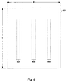
- a preferred arrangement is illustrated in the plan view of an orifice plate of FIG. 8.
- the orifice plate outer surface 801 has a cyan nozzle set 803, a cyan nozzle set 805, and a magenta nozzle set 807.
- as many as 432 drop generators are anticipated to be arranged on a printhead in the three color groups of 144 drop generators each although more or fewer can be used.
- the arrangement is such that a 1200 DPI resolution in the scan direction, X, is achieved.
- the dimensions of the semiconductor substrate to which the orifice plate is secured are shown as a width dimension, a, of nominally 7.9mm (along the X, scan, direction) and a height dimension, b, of nominally 8.7mm.
- a single color, e.g. black, printhead may employ the present invention but with different dimensions, number of primitives, and number of ink ejectors.
- the number of conductors employed in a high resolution printhead is reduced without sacrificing reliability by sharing a ground return conductor with redundant output terminals.
Priority Applications (1)
| Application Number | Priority Date | Filing Date | Title |
|---|---|---|---|
| EP04078081.9A EP1520702B1 (de) | 1999-08-30 | 2000-08-09 | Gemeinsame Erdungsrückführungen für einen Mehrfachverteiler für einen Tintenstrahldruckkopf |
Applications Claiming Priority (2)
| Application Number | Priority Date | Filing Date | Title |
|---|---|---|---|
| US386574 | 1995-02-10 | ||
| US09/386,574 US6234598B1 (en) | 1999-08-30 | 1999-08-30 | Shared multiple terminal ground returns for an inkjet printhead |
Related Child Applications (1)
| Application Number | Title | Priority Date | Filing Date |
|---|---|---|---|
| EP04078081.9A Division EP1520702B1 (de) | 1999-08-30 | 2000-08-09 | Gemeinsame Erdungsrückführungen für einen Mehrfachverteiler für einen Tintenstrahldruckkopf |
Publications (3)
| Publication Number | Publication Date |
|---|---|
| EP1080903A2 true EP1080903A2 (de) | 2001-03-07 |
| EP1080903A3 EP1080903A3 (de) | 2001-05-02 |
| EP1080903B1 EP1080903B1 (de) | 2004-11-10 |
Family
ID=23526168
Family Applications (2)
| Application Number | Title | Priority Date | Filing Date |
|---|---|---|---|
| EP00306763A Expired - Lifetime EP1080903B1 (de) | 1999-08-30 | 2000-08-09 | Gemeinsame Erdungsrückführungen für einen Mehrfachverteiler für einen Tintenstrahldruckkopf |
| EP04078081.9A Expired - Lifetime EP1520702B1 (de) | 1999-08-30 | 2000-08-09 | Gemeinsame Erdungsrückführungen für einen Mehrfachverteiler für einen Tintenstrahldruckkopf |
Family Applications After (1)
| Application Number | Title | Priority Date | Filing Date |
|---|---|---|---|
| EP04078081.9A Expired - Lifetime EP1520702B1 (de) | 1999-08-30 | 2000-08-09 | Gemeinsame Erdungsrückführungen für einen Mehrfachverteiler für einen Tintenstrahldruckkopf |
Country Status (4)
| Country | Link |
|---|---|
| US (1) | US6234598B1 (de) |
| EP (2) | EP1080903B1 (de) |
| JP (1) | JP2001080074A (de) |
| DE (1) | DE60015676T2 (de) |
Cited By (5)
| Publication number | Priority date | Publication date | Assignee | Title |
|---|---|---|---|---|
| EP1527878A1 (de) * | 2003-10-31 | 2005-05-04 | Canon Kabushiki Kaisha | Tintenstrahlaufzeichnungskopfsubstrat , Tintenstrahlaufzeichnungskopf und Tintenstrahlaufzeichnungsgerät |
| WO2005105456A2 (en) * | 2004-04-19 | 2005-11-10 | Hewlett-Packard Development Company, L.P. | Fluid ejection device |
| US7841703B2 (en) | 2004-08-23 | 2010-11-30 | Silverbrook Research Pty Ltd | Printhead having rows of symmetrically arranged nozzles |
| US7866791B2 (en) | 2004-08-23 | 2011-01-11 | Silverbrook Research Pty Ltd | Printhead having mirrored rows of print nozzles |
| EP2569163A4 (de) * | 2010-05-11 | 2018-01-24 | Hewlett Packard Development Company, L.P. | Elektrische schnittstelle für einen tintenstift |
Families Citing this family (11)
| Publication number | Priority date | Publication date | Assignee | Title |
|---|---|---|---|---|
| AUPP702498A0 (en) * | 1998-11-09 | 1998-12-03 | Silverbrook Research Pty Ltd | Image creation method and apparatus (ART77) |
| US6491377B1 (en) * | 1999-08-30 | 2002-12-10 | Hewlett-Packard Company | High print quality printhead |
| US6422676B1 (en) * | 2001-06-19 | 2002-07-23 | Hewlett-Packard Company | Compact ink jet printhead |
| US20050097385A1 (en) * | 2003-10-15 | 2005-05-05 | Ahne Adam J. | Method of fault correction for an array of fusible links |
| KR100553912B1 (ko) * | 2003-12-22 | 2006-02-24 | 삼성전자주식회사 | 잉크젯 프린트헤드 및 그 제조방법 |
| US20060092205A1 (en) * | 2004-05-27 | 2006-05-04 | Silverbrook Research Pty Ltd | Printhead module for expelling ink from nozzles in groups, starting at outside nozzles of each group |
| CA2577338C (en) * | 2004-08-23 | 2010-12-14 | Silverbrook Research Pty Ltd | Symmetric nozzle arrangement |
| EP3113953B1 (de) | 2014-03-07 | 2021-04-28 | Hewlett-Packard Development Company, L.P. | Flüssigkeitsausstossvorrichtung mit masseelektrode, die einer flüssigkeitskammer ausgesetzt ist |
| PL3183746T3 (pl) | 2014-08-18 | 2021-01-25 | Hewlett-Packard Development Company, L.P. | Alternatywne linie uziemiające do uziemienia między slotami |
| US11186082B2 (en) * | 2019-04-29 | 2021-11-30 | Hewlett-Packard Development Company, L.P. | Conductive elements electrically coupled to fluidic dies |
| US11433670B2 (en) * | 2019-04-29 | 2022-09-06 | Hewlett-Packard Development Company, L.P. | Conductive elements electrically coupled to fluidic dies |
Citations (3)
| Publication number | Priority date | Publication date | Assignee | Title |
|---|---|---|---|---|
| US5134425A (en) | 1990-01-23 | 1992-07-28 | Hewlett-Packard Company | Ohmic heating matrix |
| US5541629A (en) | 1992-10-08 | 1996-07-30 | Hewlett-Packard Company | Printhead with reduced interconnections to a printer |
| US5883650A (en) | 1995-12-06 | 1999-03-16 | Hewlett-Packard Company | Thin-film printhead device for an ink-jet printer |
Family Cites Families (21)
| Publication number | Priority date | Publication date | Assignee | Title |
|---|---|---|---|---|
| US4463359A (en) | 1979-04-02 | 1984-07-31 | Canon Kabushiki Kaisha | Droplet generating method and apparatus thereof |
| US4514741A (en) | 1982-11-22 | 1985-04-30 | Hewlett-Packard Company | Thermal ink jet printer utilizing a printhead resistor having a central cold spot |
| DE3712891A1 (de) | 1987-04-15 | 1988-11-03 | Siemens Ag | Planartintendruckkopf im dual-inline-gehaeuse |
| US4812859A (en) | 1987-09-17 | 1989-03-14 | Hewlett-Packard Company | Multi-chamber ink jet recording head for color use |
| US5212503A (en) | 1988-07-26 | 1993-05-18 | Canon Kabushiki Kaisha | Liquid jet recording head having a substrate with minimized electrode overlap |
| US4887098A (en) | 1988-11-25 | 1989-12-12 | Xerox Corporation | Thermal ink jet printer having printhead transducers with multilevelinterconnections |
| JP2705994B2 (ja) * | 1989-03-31 | 1998-01-28 | キヤノン株式会社 | 記録方法、記録装置及び記録ヘッド |
| US5030971B1 (en) | 1989-11-29 | 2000-11-28 | Xerox Corp | Precisely aligned mono- or multi-color roofshooter type printhead |
| US5103246A (en) | 1989-12-11 | 1992-04-07 | Hewlett-Packard Company | X-Y multiplex drive circuit and associated ink feed connection for maximizing packing density on thermal ink jet (TIJ) printheads |
| US5144336A (en) | 1990-01-23 | 1992-09-01 | Hewlett-Packard Company | Method and apparatus for controlling the temperature of thermal ink jet and thermal printheads that have a heating matrix system |
| US5187500A (en) * | 1990-09-05 | 1993-02-16 | Hewlett-Packard Company | Control of energy to thermal inkjet heating elements |
| US5638101A (en) | 1992-04-02 | 1997-06-10 | Hewlett-Packard Company | High density nozzle array for inkjet printhead |
| US5604519A (en) * | 1992-04-02 | 1997-02-18 | Hewlett-Packard Company | Inkjet printhead architecture for high frequency operation |
| US5357081A (en) | 1993-01-21 | 1994-10-18 | Hewlett-Packard Company | Power supply for individual control of power delivered to integrated drive thermal inkjet printhead heater resistors |
| JP3569543B2 (ja) * | 1993-03-31 | 2004-09-22 | ヒューレット・パッカード・カンパニー | 集積型印刷ヘッドのアドレス指定システム |
| US5598189A (en) | 1993-09-07 | 1997-01-28 | Hewlett-Packard Company | Bipolar integrated ink jet printhead driver |
| US5508724A (en) | 1993-09-07 | 1996-04-16 | Hewlett-Packard Company | Passive multiplexing using sparse arrays |
| US5808640A (en) | 1994-04-19 | 1998-09-15 | Hewlett-Packard Company | Special geometry ink jet resistor for high dpi/high frequency structures |
| US5635968A (en) | 1994-04-29 | 1997-06-03 | Hewlett-Packard Company | Thermal inkjet printer printhead with offset heater resistors |
| EP0786343B1 (de) * | 1996-01-23 | 2001-06-13 | Hewlett-Packard Company, A Delaware Corporation | Thermischer Tintenstrahldrucker und Ansteuerungsverfahren |
| US5835112A (en) | 1996-10-08 | 1998-11-10 | Hewlett-Packard Company | Segmented electrical distribution plane |
-
1999
- 1999-08-30 US US09/386,574 patent/US6234598B1/en not_active Expired - Lifetime
-
2000
- 2000-08-09 DE DE60015676T patent/DE60015676T2/de not_active Expired - Lifetime
- 2000-08-09 EP EP00306763A patent/EP1080903B1/de not_active Expired - Lifetime
- 2000-08-09 EP EP04078081.9A patent/EP1520702B1/de not_active Expired - Lifetime
- 2000-08-30 JP JP2000260315A patent/JP2001080074A/ja active Pending
Patent Citations (3)
| Publication number | Priority date | Publication date | Assignee | Title |
|---|---|---|---|---|
| US5134425A (en) | 1990-01-23 | 1992-07-28 | Hewlett-Packard Company | Ohmic heating matrix |
| US5541629A (en) | 1992-10-08 | 1996-07-30 | Hewlett-Packard Company | Printhead with reduced interconnections to a printer |
| US5883650A (en) | 1995-12-06 | 1999-03-16 | Hewlett-Packard Company | Thin-film printhead device for an ink-jet printer |
Cited By (10)
| Publication number | Priority date | Publication date | Assignee | Title |
|---|---|---|---|---|
| EP1527878A1 (de) * | 2003-10-31 | 2005-05-04 | Canon Kabushiki Kaisha | Tintenstrahlaufzeichnungskopfsubstrat , Tintenstrahlaufzeichnungskopf und Tintenstrahlaufzeichnungsgerät |
| WO2005105456A2 (en) * | 2004-04-19 | 2005-11-10 | Hewlett-Packard Development Company, L.P. | Fluid ejection device |
| WO2005105456A3 (en) * | 2004-04-19 | 2006-03-16 | Hewlett Packard Co | Fluid ejection device |
| US7384113B2 (en) | 2004-04-19 | 2008-06-10 | Hewlett-Packard Development Company, L.P. | Fluid ejection device with address generator |
| US7794057B2 (en) | 2004-04-19 | 2010-09-14 | Hewlett-Packard Development Company, L.P. | Fluid ejection device |
| US7841703B2 (en) | 2004-08-23 | 2010-11-30 | Silverbrook Research Pty Ltd | Printhead having rows of symmetrically arranged nozzles |
| US7866791B2 (en) | 2004-08-23 | 2011-01-11 | Silverbrook Research Pty Ltd | Printhead having mirrored rows of print nozzles |
| US8079663B2 (en) | 2004-08-23 | 2011-12-20 | Silverbrook Research Pty Ltd | Printhead having mirrored rows of print nozzles |
| US8382246B2 (en) | 2004-08-23 | 2013-02-26 | Zamtec Ltd | Printhead having mirrored rows of print nozzles |
| EP2569163A4 (de) * | 2010-05-11 | 2018-01-24 | Hewlett Packard Development Company, L.P. | Elektrische schnittstelle für einen tintenstift |
Also Published As
| Publication number | Publication date |
|---|---|
| DE60015676D1 (de) | 2004-12-16 |
| EP1520702B1 (de) | 2014-05-28 |
| DE60015676T2 (de) | 2005-10-06 |
| EP1080903A3 (de) | 2001-05-02 |
| EP1080903B1 (de) | 2004-11-10 |
| EP1520702A1 (de) | 2005-04-06 |
| JP2001080074A (ja) | 2001-03-27 |
| US6234598B1 (en) | 2001-05-22 |
Similar Documents
| Publication | Publication Date | Title |
|---|---|---|
| US6139131A (en) | High drop generator density printhead | |
| EP1080905B1 (de) | Tintenstrahltropfenerzeuger mit geteilten Widerständen zum Verringern der Stromverdichtung | |
| US7004556B2 (en) | High print quality inkjet printhead | |
| US6276775B1 (en) | Variable drop mass inkjet drop generator | |
| US6474789B1 (en) | Recording apparatus, recording head and substrate therefor | |
| US7832843B2 (en) | Liquid jet head | |
| EP1080903B1 (de) | Gemeinsame Erdungsrückführungen für einen Mehrfachverteiler für einen Tintenstrahldruckkopf | |
| US6431686B2 (en) | Fluid ejection device controlled by electrically isolated primitives | |
| JP3697089B2 (ja) | インクジェットヘッド用基体、インクジェットヘッド、インクジェットカートリッジおよびインクジェット記録装置 | |
| US7488056B2 (en) | Fluid ejection device | |
| US6123419A (en) | Segmented resistor drop generator for inkjet printing | |
| US6575562B1 (en) | Performance inkjet printhead chip layouts and assemblies | |
| US6711806B2 (en) | Method of manufacturing a thermal fluid jetting apparatus | |
| US6231165B1 (en) | Inkjet recording head and inkjet apparatus provided with the same | |
| AU734083B2 (en) | Recording apparatus, recording head and substrate therefor |
Legal Events
| Date | Code | Title | Description |
|---|---|---|---|
| PUAI | Public reference made under article 153(3) epc to a published international application that has entered the european phase |
Free format text: ORIGINAL CODE: 0009012 |
|
| AK | Designated contracting states |
Kind code of ref document: A2 Designated state(s): DE FR GB IT NL |
|
| AX | Request for extension of the european patent |
Free format text: AL;LT;LV;MK;RO;SI |
|
| PUAL | Search report despatched |
Free format text: ORIGINAL CODE: 0009013 |
|
| RIN1 | Information on inventor provided before grant (corrected) |
Inventor name: OUGHTON, DALE R. Inventor name: PRASAD, RAMA Inventor name: TORGERSON, JOSEPH M. Inventor name: CLELAND, TODD A. |
|
| AK | Designated contracting states |
Kind code of ref document: A3 Designated state(s): AT BE CH CY DE DK ES FI FR GB GR IE IT LI LU MC NL PT SE |
|
| AX | Request for extension of the european patent |
Free format text: AL;LT;LV;MK;RO;SI |
|
| RAP1 | Party data changed (applicant data changed or rights of an application transferred) |
Owner name: HEWLETT-PACKARD COMPANY, A DELAWARE CORPORATION |
|
| 17P | Request for examination filed |
Effective date: 20011010 |
|
| AKX | Designation fees paid |
Free format text: DE FR GB IT NL |
|
| GRAP | Despatch of communication of intention to grant a patent |
Free format text: ORIGINAL CODE: EPIDOSNIGR1 |
|
| GRAS | Grant fee paid |
Free format text: ORIGINAL CODE: EPIDOSNIGR3 |
|
| GRAA | (expected) grant |
Free format text: ORIGINAL CODE: 0009210 |
|
| AK | Designated contracting states |
Kind code of ref document: B1 Designated state(s): DE FR GB IT NL |
|
| REG | Reference to a national code |
Ref country code: GB Ref legal event code: FG4D |
|
| REF | Corresponds to: |
Ref document number: 60015676 Country of ref document: DE Date of ref document: 20041216 Kind code of ref document: P |
|
| PLBE | No opposition filed within time limit |
Free format text: ORIGINAL CODE: 0009261 |
|
| STAA | Information on the status of an ep patent application or granted ep patent |
Free format text: STATUS: NO OPPOSITION FILED WITHIN TIME LIMIT |
|
| ET | Fr: translation filed | ||
| 26N | No opposition filed |
Effective date: 20050811 |
|
| REG | Reference to a national code |
Ref country code: DE Ref legal event code: R082 Ref document number: 60015676 Country of ref document: DE Representative=s name: SCHOPPE, ZIMMERMANN, STOECKELER, ZINKLER & PAR, DE |
|
| REG | Reference to a national code |
Ref country code: DE Ref legal event code: R082 Ref document number: 60015676 Country of ref document: DE Representative=s name: SCHOPPE, ZIMMERMANN, STOECKELER, ZINKLER & PAR, DE Effective date: 20120229 Ref country code: DE Ref legal event code: R081 Ref document number: 60015676 Country of ref document: DE Owner name: HEWLETT-PACKARD DEVELOPMENT CO., L.P., US Free format text: FORMER OWNER: HEWLETT-PACKARD COMPANY (N.D.GES.D.STAATES DELAWARE), PALO ALTO, US Effective date: 20120229 |
|
| REG | Reference to a national code |
Ref country code: GB Ref legal event code: 732E Free format text: REGISTERED BETWEEN 20120329 AND 20120404 |
|
| REG | Reference to a national code |
Ref country code: NL Ref legal event code: SD Effective date: 20120731 |
|
| PGFP | Annual fee paid to national office [announced via postgrant information from national office to epo] |
Ref country code: GB Payment date: 20120828 Year of fee payment: 13 |
|
| PGFP | Annual fee paid to national office [announced via postgrant information from national office to epo] |
Ref country code: IT Payment date: 20120823 Year of fee payment: 13 Ref country code: DE Payment date: 20120829 Year of fee payment: 13 Ref country code: FR Payment date: 20120830 Year of fee payment: 13 |
|
| PGFP | Annual fee paid to national office [announced via postgrant information from national office to epo] |
Ref country code: NL Payment date: 20120825 Year of fee payment: 13 |
|
| REG | Reference to a national code |
Ref country code: NL Ref legal event code: V1 Effective date: 20140301 |
|
| GBPC | Gb: european patent ceased through non-payment of renewal fee |
Effective date: 20130809 |
|
| PG25 | Lapsed in a contracting state [announced via postgrant information from national office to epo] |
Ref country code: NL Free format text: LAPSE BECAUSE OF NON-PAYMENT OF DUE FEES Effective date: 20140301 Ref country code: DE Free format text: LAPSE BECAUSE OF NON-PAYMENT OF DUE FEES Effective date: 20140301 |
|
| REG | Reference to a national code |
Ref country code: DE Ref legal event code: R119 Ref document number: 60015676 Country of ref document: DE Effective date: 20140301 |
|
| REG | Reference to a national code |
Ref country code: FR Ref legal event code: ST Effective date: 20140430 |
|
| PG25 | Lapsed in a contracting state [announced via postgrant information from national office to epo] |
Ref country code: IT Free format text: LAPSE BECAUSE OF NON-PAYMENT OF DUE FEES Effective date: 20130809 |
|
| PG25 | Lapsed in a contracting state [announced via postgrant information from national office to epo] |
Ref country code: GB Free format text: LAPSE BECAUSE OF NON-PAYMENT OF DUE FEES Effective date: 20130809 |
|
| PG25 | Lapsed in a contracting state [announced via postgrant information from national office to epo] |
Ref country code: FR Free format text: LAPSE BECAUSE OF NON-PAYMENT OF DUE FEES Effective date: 20130902 |