EP1077472A2 - Etching apparatus - Google Patents
Etching apparatus Download PDFInfo
- Publication number
- EP1077472A2 EP1077472A2 EP00117663A EP00117663A EP1077472A2 EP 1077472 A2 EP1077472 A2 EP 1077472A2 EP 00117663 A EP00117663 A EP 00117663A EP 00117663 A EP00117663 A EP 00117663A EP 1077472 A2 EP1077472 A2 EP 1077472A2
- Authority
- EP
- European Patent Office
- Prior art keywords
- wafer
- frame
- wafer frame
- cassette
- etching
- Prior art date
- Legal status (The legal status is an assumption and is not a legal conclusion. Google has not performed a legal analysis and makes no representation as to the accuracy of the status listed.)
- Granted
Links
Images

Classifications
-
- H—ELECTRICITY
- H10—SEMICONDUCTOR DEVICES; ELECTRIC SOLID-STATE DEVICES NOT OTHERWISE PROVIDED FOR
- H10P—GENERIC PROCESSES OR APPARATUS FOR THE MANUFACTURE OR TREATMENT OF DEVICES COVERED BY CLASS H10
- H10P72/00—Handling or holding of wafers, substrates or devices during manufacture or treatment thereof
- H10P72/04—Apparatus for manufacture or treatment
- H10P72/0451—Apparatus for manufacturing or treating in a plurality of work-stations
- H10P72/0468—Apparatus for manufacturing or treating in a plurality of work-stations comprising a chamber adapted to a particular process
-
- H—ELECTRICITY
- H10—SEMICONDUCTOR DEVICES; ELECTRIC SOLID-STATE DEVICES NOT OTHERWISE PROVIDED FOR
- H10P—GENERIC PROCESSES OR APPARATUS FOR THE MANUFACTURE OR TREATMENT OF DEVICES COVERED BY CLASS H10
- H10P72/00—Handling or holding of wafers, substrates or devices during manufacture or treatment thereof
- H10P72/04—Apparatus for manufacture or treatment
- H10P72/0402—Apparatus for fluid treatment
- H10P72/0418—Apparatus for fluid treatment for etching
- H10P72/0422—Apparatus for fluid treatment for etching for wet etching
- H10P72/0424—Apparatus for fluid treatment for etching for wet etching using mainly spraying means, e.g. nozzles
-
- H—ELECTRICITY
- H10—SEMICONDUCTOR DEVICES; ELECTRIC SOLID-STATE DEVICES NOT OTHERWISE PROVIDED FOR
- H10P—GENERIC PROCESSES OR APPARATUS FOR THE MANUFACTURE OR TREATMENT OF DEVICES COVERED BY CLASS H10
- H10P72/00—Handling or holding of wafers, substrates or devices during manufacture or treatment thereof
- H10P72/04—Apparatus for manufacture or treatment
- H10P72/0442—Apparatus for placing on an insulating substrate, e.g. tape
Definitions
- the present invention relates to an etching apparatus, more particularly to an etching apparatus which etches a wafer, of which reverse has been ground by a planarization apparatus, and then automatically mounts the wafer on a wafer frame for dicing.
- a fracture layer is formed on the reverse of the semiconductor wafer by the back grinding, and the fracture layer results in lower strength of the semiconductor wafer.
- the ground reverse of the semiconductor wafer is processed with an etching process in order to remove the fracture layer.
- the semiconductor wafer that is etched after the back grinding as described above is mounted on a wafer frame after separating a protecting sheet, which is adhered for protecting the obverse of the wafer at back grinding. Then, the semiconductor wafer is supplied to a dicing machine while being mounted on the wafer frame, and the semiconductor wafer is diced into individual elements by the dicing machine.
- the present invention has been developed in view of the above-described circumstances, and has as its object the provision of an etching apparatus that can automatically mount the etched wafer on the wafer frame.
- the present invention is directed to an etching apparatus, comprising: an etching part which holds an obverse of a wafer with a chuck by suction, the chuck being movable up and down and rotatable, then supplies etching liquid to a reverse of the wafer while rotating the wafer in a processing vessel so as to etch the reverse of the wafer, then jets a cleaning liquid to the reverse of the wafer while rotating the wafer so as to clean the reverse of the wafer, and then jets air to the reverse of the wafer while rotating the wafer so as to dry the reverse of the wafer; a wafer supply part which supplies the wafer to the etching part; a mount part which receives a wafer frame at a wafer frame receiving position, then moves relatively to an upper part of the processing vessel, then mounts the wafer on the wafer frame by adhering the reverse of the wafer that is transported to the upper part by the chuck to an adhesive sheet together with the wafer frame
- the wafer is first supplied to the etching part by the wafer supply part.
- the obverse of the wafer, supplied to the etching part, is held by suction with the chuck which can move up and down and can rotate.
- the wafer is rotated in the processing vessel while the etching liquid is supplied to the reverse of the wafer so as to etch the wafer.
- the wafer is again rotated in the processing vessel while the cleaning liquid is jetted to the reverse of the wafer so as to clean the wafer.
- the cleaned wafer is still again rotated in the processing vessel while the air is supplied to the reverse of the wafer so as to dry the wafer.
- the mount part which has received the wafer frame from the wafer frame supply part at the wafer frame receiving position moves to the upper part of the processing vessel. Then, the chuck moves up to the mount part which has moved to the upper part of the processing vessel, and the reverse of the wafer is adhered to the adhesive sheet together with the wafer frame, thereby the wafer is mounted on the wafer frame.
- the mount part that includes the wafer frame and the wafer mounted on the wafer frame returns to the wafer frame receiving position, and the wafer frame collecting part collects the wafer frame from the mount part that has returned to the wafer frame receiving position.
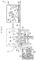
- Fig. 1 is a plan view showing an entire construction of an etching apparatus according to the first embodiment of the present invention.
- the etching apparatus 10 comprises a wafer supply part 12, an etching part 14, a mount part 16, a wafer frame supply part 18, and a wafer frame collection part 20.
- the wafer supply part 12 serves to supply a wafer W to be processed to the etching part 14.
- the wafer supply part 12 comprises a wafer cassette stage 22, an alignment device 24, and a wafer transport robot 26.
- a wafer cassette 28 that stores a number of wafers W to be processed is set at the wafer cassette stage 22.
- the alignment device 24 aligns the wafer W that is supplied to the etching part 14.
- the alignment device 24 comprises a measurement table 30 and an alignment sensor 32.
- the wafer W is held by suction to the measurement table 30 and is rotated, and the alignment sensor 32 detects an orientation flat or a position of a notch, which is formed on the wafer W, and the center of the wafer W.
- the wafer W is then aligned based on the results of the detection; more specifically, the measurement table 30 rotates such that the orientation flat or the notch is directed in a predetermined direction, and the wafer W is transported to the wafer transport robot 26 so that the center of the wafer W corresponds with the center of a chuck table 42 of the etching part 14.
- the wafer transport robot 26 transports the wafer W from the wafer cassette 28 to the alignment device 24 and also transports the wafer W from the alignment device 24 to the etching part 14.
- the wafer transport robot is a common industrial robot, which comprises an arm 34 and a suction pad 36, which is provided at the end of the arm 34.
- the arm 34 comprises a first arm 34A and a second arm 34B.
- the first arm 34A can swivel around the base part and move up and down.
- the suction pad 36 is rotatably provided to the end of the second arm 34B, and the wafer W is held by the suction pad 36 and transported.
- the wafer transport robot 26 picks up the wafer W from the wafer cassette 28, which is set at the wafer cassette stage 22, and transports the wafer W to the alignment device 24.
- the wafer W is aligned by the alignment device 24 and is supplied to the etching part 14.
- the construction of the etching part 14 shown in Fig. 2 is described.
- the etching part 14 etches the reverse of the wafer W (opposite of the obverse, on which a circuit pattern is formed).
- the etching part 14 comprises a processing vessel 40, the chuck table 42, and a supply apparatus 44.
- the processing vessel 40 is formed in a cylindrical shape, and the chuck table 42 is arranged in the processing vessel 40.
- the chuck table 42 is formed like a disk, and serves to hold the obverse of the wafer W (the face on which the circuit pattern is formed) by suction.
- the chuck table 42 is rotated by a rotation means (not shown), and is also driven by an elevation means (not shown) to move up and down.
- the supply apparatus 44 comprises an arm 46 and a nozzle 48, which is provided at the end of the arm 46.
- the arm 46 is driven by a swivel means (not shown) and swivels so as to position the nozzle 48 at a supply position, which is the upper position of the chuck table 42 as shown in Fig.
- a etching liquid supplying device 50, a cleaning liquid supplying device 52, and an air supplying device 54 are connected to the nozzle 48 through pipes, and they are constructed to selectively supply one of etching liquid, cleaning liquid and air to the nozzle 48.
- the wafer W is etched by the process presented below.
- the wafer W that is transported from the alignment device 24 to the etching part 14 by the wafer transport robot 26 is placed on the chuck table 42, which is positioned at a predetermined wafer receiving position. At this point, the wafer W is placed on the chuck table 42 so that the obverse of the wafer W is turned down, and the orientation flat or the notch is directed in the predetermined direction.
- the chuck table 42 holds the wafer W by suction, and the chuck table 42 descends by a predetermined amount and positions at a predetermined etching position (the position in Fig. 2).
- the arm 46 When the chuck table 42 positions at the etching position, the arm 46 swivels so that the nozzle 48 moves from the stand-by position to the supply position while swinging between the stand-by position and the supply position.
- the etching liquid supplying device 50 and the rotation drive means are then driven, whereby the etching liquid is evenly supplied from the nozzle 48 to the reverse of the rotating wafer W while the arm 46 swings, so that the reverse of the wafer W is etched.
- the driving of the etching liquid supplying device 50 is stopped.
- the cleaning liquid supplying device 52 is then driven, whereby the cleaning liquid is jetted from the nozzle 48 to the reverse of the rotating wafer W, so that the reverse of the etched wafer W is cleaned.
- the driving of the cleaning liquid supplying device 52 is stopped.
- the air supplying device 54 is then driven, whereby the air is jetted from the nozzle 48 to the reverse of the rotating wafer W, so that the reverse of the cleaned wafer W is dried.
- the driving of the air supplying device 54 is stopped.
- the arm 46 is then swiveled to return the nozzle 48 to the stand-by position, and the driving of the rotation drive means is stopped to stop the rotation of the chuck table 42.
- the chuck table 42 stops at the position where the orientation flat or the notch, which is detected by the rotation position detector (not shown), is directed in the predetermined direction.
- the mount part 16 serves to mount the etched wafer W on a wafer frame F for dicing. More specifically, the mount part 16 mounts the wafer W on the wafer frame F for dicing through a wafer sheet S.
- the mount part 16 comprises a moving body 60, a holder 62, a wafer sheet adhering device 64 and a wafer sheet cutting device 66.
- the moving body 60 is slidably provided on guide rails 68, and is driven by a moving device (not shown) (e.g. a leading screw mechanism or a cylinder) so as to move along the guide rails 68.
- the moving body 60 reciprocally moves between the predetermined wafer frame receiving position and the mounting position, which is set at the upper part of the processing vessel 40.
- the holder 62 is provided on the moving body 60, and holds the wafer frame F.
- the wafer sheet adhering device 64 and the wafer sheet cutting device 66 are provided on the moving body 60.
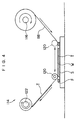
- the wafer sheet adhering device 64 comprises a wafer sheet supply roller 70, around which a strip wafer sheet S is wound, a wafer sheet wind-up roller 72 for winding up the wafer sheet S that is fed from the wafer sheet supply roller 70, and a wafer sheet pressing roller 74 for pressing the wafer sheet S against the top faces of the wafer W and the wafer frame F so as to adhere the wafer sheet S.
- the wafer sheet cutting device 66 comprises a cutting arm 76, which can rotate as well as move up and down, and a cutting blade 78, which is provided at the end of the cutting arm 76.
- the wafer W is mounted on the wafer frame F by the following process.
- the wafer frame F is supplied from the wafer frame supply part 18, which will be described later, to the mount part 16, which is positioned at the wafer frame receiving position, and the wafer W is placed on the holder 62.
- the moving body 60 moves to the mounting position.
- the wafer frame F that is held by the holder 62 corresponds with the center of the wafer W held on the chuck table 42.
- the chuck table 42 ascends and moves to a predetermined adhering position. At this state, the reverse of the wafer W (top face) is flush with the top face of the wafer frame F.
- the wafer sheet pressing roller 74 descends by the predetermined amount and presses the wafer sheet S against the wafer frame F.
- the wafer sheet pressing roller 74 then moves along the top face of the wafer frame F so as to adhere the wafer sheet S on the top faces of the wafer W and the wafer frame F.
- the cutting arm 76 descends by the predetermined amount and presses the edge of the cutting blade 78 against the top face of the wafer frame F, then rotates, whereby an extra portion of the outer periphery of the wafer sheet S that is adhered to the wafer frame F is cut out by the cutting blade 78.
- the cutting arm 76 ascends by the predetermined amount, and the wafer sheet pressing roller 74 returns to its original position. Then, the wafer sheet wind-up roller 72 is driven so that the extra portion of the wafer sheet S that is cut out is wound up by the wafer sheet wind-up roller 72.
- the chuck table 42 releases the wafer W from the suction and descends by the predetermined amount so as to move to the predetermined stand-by position.
- the mounting process for the wafer W is completed through the above-described process. After the completion of the mounting process, the moving body 60 returns to the wafer frame receiving position.
- the wafer frame supply part 18 supplies the wafer frame F to the holder 62 of the mount part 16 that is positioned at the wafer frame receiving position.
- the wafer frame supply part 18 comprises a wafer frame stocker 80 and a wafer frame supply robot (not shown).
- the wafer frame stocker 80 contains wafer frames F in piled state, and the wafer frame supply robot transports the wafer frames F onto the holder 62 of the mount part 16 that is positioned at the wafer frame receiving position.
- the wafer frame collecting part 20 serves to collect the wafer frames F from the holder 62 of the mount part 16 that has returned to the wafer frame receiving position after mounting the wafer W.
- the wafer collecting part 20 comprises a wafer frame cassette stage 82 and a wafer frame collecting robot 84.
- a wafer frame cassette 86 is set in which number of the wafer frames F on that the wafers W are mounted can be stored.
- the wafer frame collecting robot 84 picks up the wafer frame F from the holder 62 of the mount part 16 that has returned to the wafer frame receiving position, and stores the wafer frame F in the wafer frame cassette 86 that is set on the wafer frame cassette stage 82.
- the wafer frame collecting robot 84 is a common industrial robot, which comprises an arm 88 and a damper (not shown), which is provided at the end of the arm 88.
- the arm 88 comprises a first arm 88A and a second arm 88B.
- the first arm 88A can swivel around the base part and move up and down.
- the second arm 88B is provided at the end of the first arm 88A.
- the clamper is provided at the end of the second arm 88B, and the wafer frame F is grasped by the damper and transported.
- the operator sets the wafer cassette 28 that stores a number of wafers W to be etched on the wafer cassette stage 22.
- the wafer frame F is set next in the wafer frame stocker 80.
- the operator sets the empty wafer frame cassette 86 on the wafer frame cassette stage 82.
- the etching apparatus 10 is activated.
- the wafer transport robot 26 first picks up the wafer W from the wafer cassette 28, and transports the picked-up wafer W onto the measurement table 30 of the alignment device 24.
- the alignment device 24 aligns the transported wafer W, and after completion of the aligning, the wafer transport robot 26 picks up the wafer W from the measurement table 30 and transports then to the etching part 14.
- the wafer W that is transported to the etching part 14 by the wafer transport robot 26 is placed on the chuck table 42 that positions at the predetermined wafer receiving position. At this point, the wafer W is placed on the chuck table 42 so that the obverse of the wafer is turned down and the orientation flat or the notch is directed in the predetermined direction.
- the chuck table 42 holds the wafer W by suction, and descends by the predetermined amount so as to position at the etching position.
- the etching process starts. First, the arm 46 swivels so that the nozzle 48 swings from the stand-by position to the supply position. Then, the etching liquid supplying device 50 is driven and the etching liquid is supplied to the wafer W on the chuck table 42. At the same time, the rotation drive means is driven so that the chuck table 42 rotates. Thus, the etching liquid is jetted to the reverse (now the top face) of the rotating wafer W and the reverse of the wafer W is etched.
- the driving of the etching liquid supplying device 50 is stopped, and the cleaning liquid supplying device 52 is driven, whereby the cleaning liquid is jetted from the nozzle 48 to the reverse of the rotating wafer W and the reverse of the etched wafer W is cleaned.
- the driving of the cleaning liquid supplying device 52 is stopped, and the air supplying device 54 is driven next, whereby the air is jetted from the nozzle 48 to the rotating wafer W and the reverse of the cleaned wafer W is dried.
- the driving of the air supplying device 54 is stopped.
- the arm 46 swivels so that the nozzle 48 returns to the stand-by position.
- the driving of the rotation drive means is stopped so as to stop the rotation of the chuck table 42.
- the wafer frame supply robot (not shown) of the wafer frame supply part 18 picks up the wafer frame F from the wafer frame stocker 80, and places the wafer frame F on the holder 62 of the mount part 16 that is positioned at the wafer frame receiving position. Then, the moving body 60 moves to the mounting position as shown with an alternate long and two short dashes line in Fig. 2, that is, the upper part of the processing vessel 40.
- the chuck table 42 ascends to the predetermined adhering position. Thereby, the reverse of the wafer W (now the top face) becomes flush with the top face of the wafer frame F.
- the wafer sheet S is then adhered to the top faces of the wafer W and the wafer frame F.
- the wafer sheet pressing roller 74 descends by the predetermined amount and presses the wafer sheet S against the wafer frame F, and further moves along the top face of the wafer frame F so as to adhere the wafer sheet S to the top faces of the wafer W and the wafer frame F.
- the cutting arm 76 descends by the predetermined amount and rotates, whereby the extra outer periphery of the wafer sheet S that is adhered to the wafer frame F is cut out by the cutting blade 78, which is provided at the end of the cutting arm 76. After that, the cutting arm 76 ascends by the predetermined amount and returns to its original position.
- the wafer sheet pressing roller 74 as well returns to its original position and the extra wafer sheet S that is cut out is wound up by the wafer sheet wind-up roller 72.
- the chuck table 42 releases the wafer W from the suction, and descends by the predetermined amount so as to return at the predetermined stand-by position. Thus, the wafer W is mounted on the wafer frame F.
- the moving body 60 When the wafer W is mounted on the wafer frame F, the moving body 60 returns to the wafer frame receiving position.
- the wafer frame collecting robot 84 picks up the wafer frame F from the holder 62 of the mount part 16 that has returned to the wafer frame receiving position, and stores the wafer frame F in the wafer frame cassette 86 that is set on the wafer frame cassette stage 82.
- Wafers W that are stored in the wafer cassette 28 are sequentially processed in an order by the same process.
- the wafer W stored in the wafer cassette 28 is etched, mounted on the wafer frame F, and is stored in the wafer frame cassette 86, all in an automatic manner.
- the processing efficiency can be dramatically improved.
- the etched wafer is extremely thin and is extremely difficult to handle; however, the wafer W is mounted on the wafer frame F at the etching part 14 in the present invention, so that the handling can be easily performed and the yield can be improved as a result.
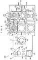
- Fig. 3 is a plan view showing an entire construction of an etching apparatus according to the second embodiment of the present invention.
- the etching apparatus 10 stores the wafer frame F in the wafer frame cassette 86 just after mounting the wafer W on the wafer frame F.
- the protecting sheet T is adhered to the obverse of etched wafer W, and the protecting sheet T must be separated from the wafer W before the next dicing process.
- the etching apparatus 100 in the second embodiment stores the wafer W mounted on the wafer frame F in the wafer frame cassette after removing the protecting sheet T from the wafer W and cleaning the wafer W.
- the collecting part of the etching apparatus 100 in the second embodiment comprises a protecting sheet separation device 102, a cleaning device 104, a wafer frame stage 106, a first wafer frame transport robot 108, and a second wafer frame transport robot 110.
- the protecting sheet separation device 102 separates the protecting sheet T from the obverse of the wafer W that is mounted on the wafer frame F.
- the protecting sheet separation device 102 comprises a ultraviolet (UV) irradiation unit 112 and a protecting sheet separation unit 114.
- UV ultraviolet
- the obverse of the wafer W is dried by blowing air, and then the UV-irradiation unit 12 irradiates the obverse of the wafer W with UV light.
- adhesive of the protecting sheet T which is adhered to the obverse of the wafer W, is hardened by irradiation of UV light.
- the protecting sheet separation unit 114 removes the protecting sheet T that is adhered to the obverse of the wafer W.
- the protecting sheet separation unit 114 adheres an adhesion tape 118, which is fed from an adhesion tape supply roller 116 with the adhering face turned down, onto the protecting sheet T over the obverse of the wafer W by an adhesion tape pressing roller 120.
- an adhesion tape wind-up roller 122 winds up the adhesion tape 118 along with the protecting sheet T, so that the protecting sheet T is removed from the obverse of the wafer W.
- the cleaning device 104 cleans by jet scrubbing the obverse of the wafer W from which the protecting sheet T is removed. More specifically, the wafer W is held on a turn table, which is disposed in a cleaning vessel, and the cleaning liquid is jetted to the wafer while rotating the wafer W so as to rinse the wafer W. Then, a rotating brush is pressed against the obverse of the rotating wafer W so as to clean the wafer W by scrubbing, and after that, the cleaning liquid is jetted in a low pressure while still rotating the wafer W so as to clean the wafer W by the low-pressurized jet cleaning. Thereafter, the cleaning liquid is jetted so as to rinse the wafer W while rotating the wafer W, and the air is at last jetted to the still rotating wafer W so as to dry the wafer by spin drying.
- a wafer frame cassette 124 is set, which can store a number of wafer frames F on which the wafers W are mounted.
- the first wafer frame transport robot 108 picks up the wafer frame F from the holder 62 of the mount part 16 that is positioned at the wafer frame receiving position, and turns the wafer frame F upside down, then transports the wafer frame F to the UV irradiation unit 112.
- the first wafer frame transport robot 108 also transports the wafer frame F from the UV irradiation unit 112 to the protecting sheet separation unit 114.
- the first wafer frame transport robot 108 is a common industrial robot, which comprises an arm 126 and a clamper (not shown), which is provided to the end of the arm 126.
- the arm 126 comprises a first arm 126A, a second arm 126B, and a third arm 126C.
- the first arm 126A can swivel around the base part and move up and down.
- the second arm 126B is provided to the end of the first arm 126A to be able to swivel
- the third arm 126C is provided to the end of the arm 126B to be able to swivel.
- the damper is provided to the end of the third arm 126C to be rotatable around the axis of the third arm 126C.
- the wafer frame F is clamped by the damper and is transported. The wafer frame F is turned upside down by rotating the damper by the half amount around the axis of the third arm 126C.
- the second wafer frame transport robot 110 transports the wafer frame F from the protecting sheet separation unit 114 to the cleaning device 104 as well as collecting the wafer frame F from the cleaning device 104, and stores the wafer frame F in the wafer frame cassette 124 that is set on the wafer frame stage 106.
- the second wafer frame transport robot 110 is another common industrial robot, which is the same as the first wafer frame transport robot 108 and comprises an arm 128 and a clamper (not shown), which is provided to the end of the arm 128.
- the arm 128 comprises a first arm 128A, a second arm 128B, and a third arm 128C.
- the first arm 128A can swivel around the base part and move up and down.
- the second arm 128B is provided to the end of the first arm 128A to be able to swivel
- the third arm 128C is provided to the end of the second arm 18B to be able to swivel.
- the clamper is provided to the end of the third arm 128C, and the wafer frame F is clamped by the damper and is transported.
- the first wafer frame transport robot 108 picks up the wafer frame F from the holder 62 of the mount part 16. Then, the wafer frame F is turned upside down, and is transported to the UV irradiation position in the UV irradiation unit 112.
- the UV irradiation unit 112 When the wafer frame F is transported to the UV irradiation position, the UV irradiation unit 112 first blows the air to dry the obverse of the wafer W, then irradiates the obverse of the wafer W with UV light. After the irradiating is completed, the first wafer frame transport robot 108 transports the wafer frame F to the protecting sheet separation unit 114. The protecting sheet separation unit 114 removes the protecting sheet T from the obverse of the wafer W that is mounted on the transported wafer frame F.
- the second wafer frame transport robot 110 transports the wafer frame F to the cleaning device 104, which cleans the obverse of the wafer W that is mounted on the transported wafer frame F by the jet scrubbing.
- the second wafer frame transport robot 110 collects the wafer frame F from the cleaning device 104, and stores the wafer frame F in the wafer frame cassette 124 that is set on the wafer frame stage 106.
- the etched wafer W is mounted on the wafer frame F and the protecting sheet T is removed from the obverse of the wafer W, then the wafer W is stored in the wafer frame cassette 124.
- the protecting sheet T does not have to be removed by an additional process and by an additional apparatus after mounting the wafer W on the wafer frame F, and hence the processing efficiency can be further improved.
- the obverse of the wafer W is cleaned by the cleaning device 104 after removing the protecting sheet T; thus the contamination on the pattern face can be eliminated.
- the etching apparatus may be constructed in a manner to store the wafer W in the wafer frame cassette 124 just after removing the protecting sheet T without the cleaning device 104.
- the transporting of the wafer frame F from the mount part 16 to the UV irradiation unit 112 and the transporting of the wafer frame F from the UV irradiation unit 112 to the protecting sheet separation unit 114 are both performed by the first wafer frame transport robot 108, but may also be performed by two transport robots provided individually. Further, the transporting of the wafer frame F from the protecting sheet separation unit 114 to the cleaning device 104 and the transporting of the wafer frame F from the cleaning device 104 to the wafer frame cassette 124 are both performed by the second wafer frame transport robot 110, but may also be performed by two transporting robots provided individually. Other transport means instead of the transport robots may be used.
- the wafer is etched and the etched wafer is mounted on the wafer frame all in an automatic manner. Therefore, the present invention can handle the extremely thin wafer more safely and can improve the yield while the processing efficiency is dramatically improved.
Landscapes
- Weting (AREA)
- Container, Conveyance, Adherence, Positioning, Of Wafer (AREA)
- Dicing (AREA)
Abstract
Description
Claims (6)
- An etching apparatus (10, 100), comprising:an etching part (14) which holds an obverse of a wafer (W) with a chuck (42) by suction, the chuck (42) being movable up and down and rotatable, then supplies etching liquid to a reverse of the wafer (W) while rotating the wafer (W) in a processing vessel (40) so as to etch the reverse of the wafer (W), then jets a cleaning liquid to the reverse of the wafer (W) while rotating the wafer (W) so as to clean the reverse of the wafer (W), and then jets air to the reverse of the wafer (W) while rotating the wafer (W) so as to dry the reverse of the wafer (W);a wafer supply part (12) which supplies the wafer (W) to the etching part (14);a mount part (16) which receives a wafer frame (F) at a wafer frame receiving position, then moves relatively to an upper part of the processing vessel (40), then mounts the wafer (W) on the wafer frame (F) by adhering the reverse of the wafer (W) that is transported to the upper part by the chuck (42) to an adhesive sheet (S) together with the wafer frame (F) so as to mount the wafer (W) on the wafer frame (F), and then returns to the wafer frame receiving position;a wafer frame supply part (18) which supplies the wafer frame (F) to the mount part (16) which is positioned at the wafer frame receiving position; anda wafer frame collection part (20) which collects the wafer frame (F) from the mount part (16) having returned at the wafer frame receiving position.
- The etching apparatus (10, 100) as defined in claim 1, wherein the wafer supply part (12) comprises:a wafer cassette stage (22) to which a wafer cassette (28) is placed, a plurality of wafers (W) being stored in the wafer cassette (28); anda wafer transporting device (26) which picks up the wafer (W) from the wafer cassette (28) placed at the wafer cassette stage (22) and supplies the wafer (W) to the etching part (14).
- The etching apparatus (10, 100) as defined in claim 2, wherein:the wafer supply part (12) further comprises an alignment device (24) which aligns the wafer (W); andthe wafer transporting device (26) transports the wafer (W) picked up from the wafer cassette (28) to the alignment device (24) and supplies the wafer (W) aligned by the alignment device (24) to the etching part (14).
- The etching apparatus (10, 100) as defined in one of claims 1, 2 and 3, wherein the wafer frame collection part (20) comprises:a wafer frame cassette stage (82) to which a wafer frame cassette (86) is placed, a plurality of wafer frames (F) being stored in the wafer frame cassette (86); anda wafer frame transporting device (84) which collects the wafer frame (F) from the mount part (16) having returned to the wafer frame receiving position and stores the wafer frame (F) in the wafer frame cassette (86) placed at the wafer frame cassette stage (82).
- The etching apparatus (100) as defined in one of claims 1, 2 and 3, wherein the wafer frame collection part (20) comprises:a protecting sheet separation device (102) which removes a protecting sheet (T) adhered to the obverse of the wafer (W) mounted on the wafer frame (F);a wafer frame cassette stage (106) to which a wafer frame cassette (124) is placed, a plurality of wafer frames (F) being stored in the wafer frame cassette (124);a first wafer frame transporting device (108) which collects the wafer frame (F) from the mount part (16) having returned to the wafer frame receiving position and transports the wafer frame (F) to the protecting sheet separation device (102); anda second wafer frame transporting device (110) which stores the wafer frame in the wafer frame cassette (124) placed at the wafer frame cassette stage (106), the protecting sheet (T) of the obverse of the wafer (W) mounted on the wafer frame (F) having been removed by the protecting sheet separation device (124).
- The etching apparatus (100) as defined in one of claims 1, 2 and 3, wherein the wafer frame collection part comprises:a protecting sheet separation device (102) which removes a protecting sheet (T) adhered to the obverse of the wafer (W) mounted on the wafer frame (F);a wafer cleaning device (104) which cleans the obverse of the wafer (W) from which the protecting sheet (T) has been removed;a wafer frame cassette stage (106) to which a wafer frame cassette (124) is placed, a plurality of wafer frames (F) being stored in the wafer frame cassette (124);a first wafer frame transporting device (108) which collects the wafer frame (F) from the mount part (16) having returned to the wafer frame receiving position and transports the wafer frame (F) to the protecting sheet separation device (102);a second wafer frame transporting device (110) which transports the wafer frame (F) to the wafer cleaning device (104), the protecting sheet (T) of the obverse of the wafer (W) mounted on the wafer frame (F) having been removed by the protecting sheet separation device (102); anda third wafer frame transporting device (110) which stores the wafer frame (F) in the wafer frame cassette (124) placed at the wafer frame cassette stage (106), the obverse of the wafer (W) mounted on the wafer frame (F) having been cleaned by the wafer cleaning device (104).
Applications Claiming Priority (2)
| Application Number | Priority Date | Filing Date | Title |
|---|---|---|---|
| JP23219099 | 1999-08-19 | ||
| JP23219099A JP3348700B2 (en) | 1999-08-19 | 1999-08-19 | Etching equipment |
Publications (3)
| Publication Number | Publication Date |
|---|---|
| EP1077472A2 true EP1077472A2 (en) | 2001-02-21 |
| EP1077472A3 EP1077472A3 (en) | 2006-01-18 |
| EP1077472B1 EP1077472B1 (en) | 2006-12-20 |
Family
ID=16935413
Family Applications (1)
| Application Number | Title | Priority Date | Filing Date |
|---|---|---|---|
| EP00117663A Expired - Lifetime EP1077472B1 (en) | 1999-08-19 | 2000-08-16 | Etching apparatus |
Country Status (4)
| Country | Link |
|---|---|
| US (1) | US6569282B1 (en) |
| EP (1) | EP1077472B1 (en) |
| JP (1) | JP3348700B2 (en) |
| DE (1) | DE60032425T2 (en) |
Families Citing this family (17)
| Publication number | Priority date | Publication date | Assignee | Title |
|---|---|---|---|---|
| JP2002343756A (en) * | 2001-05-21 | 2002-11-29 | Tokyo Seimitsu Co Ltd | Wafer flat surface processing equipment |
| AT502233B1 (en) * | 2001-06-07 | 2007-04-15 | Thallner Erich | DEVICE FOR RELEASING A SUPPORT FROM A SEMICONDUCTOR DISC |
| JP2003007648A (en) * | 2001-06-18 | 2003-01-10 | Disco Abrasive Syst Ltd | Semiconductor wafer splitting system |
| US20030230323A1 (en) * | 2002-06-14 | 2003-12-18 | Taiwan Semiconductor Manufacturing Co., Ltd. | Apparatus and method for improving scrubber cleaning |
| JP2005276987A (en) * | 2004-03-24 | 2005-10-06 | Lintec Corp | Ultra-thin chip manufacturing process and manufacturing equipment |
| US7644512B1 (en) * | 2006-01-18 | 2010-01-12 | Akrion, Inc. | Systems and methods for drying a rotating substrate |
| KR100876155B1 (en) * | 2006-11-28 | 2008-12-26 | 삼성전자주식회사 | Wafer protective tape cutting device, back lapping equipment and wafer protective tape cutting method using the same |
| JP4964107B2 (en) * | 2007-12-03 | 2012-06-27 | 東京応化工業株式会社 | Peeling device |
| US8642448B2 (en) | 2010-06-22 | 2014-02-04 | Applied Materials, Inc. | Wafer dicing using femtosecond-based laser and plasma etch |
| US8703581B2 (en) * | 2011-06-15 | 2014-04-22 | Applied Materials, Inc. | Water soluble mask for substrate dicing by laser and plasma etch |
| US8834662B2 (en) * | 2012-03-22 | 2014-09-16 | Taiwan Semiconductor Manufacturing Company, Ltd. | Apparatus and method of separating wafer from carrier |
| JP6099118B2 (en) * | 2012-04-26 | 2017-03-22 | Necエンジニアリング株式会社 | Sheet pasting system and sheet pasting method |
| JP6166872B2 (en) * | 2012-07-27 | 2017-07-19 | リンテック株式会社 | Sheet sticking device and sheet sticking method |
| KR102559647B1 (en) * | 2016-08-12 | 2023-07-25 | 삼성디스플레이 주식회사 | Substrate polishing system and substrate polishing method |
| KR101901139B1 (en) * | 2016-12-29 | 2018-09-21 | 주식회사 에스에프에이 | a cooling-type glass transfer device and etching apparatus having the same |
| DE102018109531A1 (en) * | 2018-04-20 | 2019-10-24 | Christian-Albrechts-Universität Zu Kiel | Adhesive joining device and adhesive joining method for a metallic surface |
| US11889742B2 (en) * | 2020-11-04 | 2024-01-30 | Samsung Display Co., Ltd. | Apparatus of manufacturing display device and method of manufacturing display device |
Family Cites Families (14)
| Publication number | Priority date | Publication date | Assignee | Title |
|---|---|---|---|---|
| JP2598305B2 (en) * | 1988-06-06 | 1997-04-09 | 日東電工株式会社 | Semiconductor wafer processing system |
| JPH06302572A (en) | 1993-04-12 | 1994-10-28 | Hitachi Ltd | Manufacture of semiconductor device and tape adhering and peeling apparatus |
| US5474647A (en) * | 1993-11-15 | 1995-12-12 | Hughes Aircraft Company | Wafer flow architecture for production wafer processing |
| US5590445A (en) * | 1994-03-22 | 1997-01-07 | Teikoku Seiki Kabushiki Kaisha | Tape extension device for semiconductor producing apparatus and semiconductor producing apparatus with tape extension device |
| US5672239A (en) * | 1995-05-10 | 1997-09-30 | Tegal Corporation | Integrated semiconductor wafer processing system |
| KR19990028523A (en) * | 1995-08-31 | 1999-04-15 | 야마모토 히데키 | Method for peeling protective adhesive tape of semiconductor wafer and its device |
| US6239038B1 (en) * | 1995-10-13 | 2001-05-29 | Ziying Wen | Method for chemical processing semiconductor wafers |
| JPH09223680A (en) | 1996-02-16 | 1997-08-26 | Disco Abrasive Syst Ltd | Polishing device with etching function |
| JPH10163135A (en) | 1996-12-05 | 1998-06-19 | Disco Abrasive Syst Ltd | Semiconductor processing sheet, dicing method and polishing method using the sheet |
| US6149758A (en) * | 1997-06-20 | 2000-11-21 | Lintec Corporation | Sheet removing apparatus and method |
| US6218727B1 (en) * | 1997-08-07 | 2001-04-17 | Infineon Technologie Ag | Wafer frame |
| JP3993918B2 (en) * | 1997-08-25 | 2007-10-17 | 富士通株式会社 | Manufacturing method of semiconductor device |
| JP3888754B2 (en) | 1997-12-08 | 2007-03-07 | 日東電工株式会社 | Automatic semiconductor wafer pasting equipment |
| JP3560823B2 (en) * | 1998-08-18 | 2004-09-02 | リンテック株式会社 | Wafer transfer device |
-
1999
- 1999-08-19 JP JP23219099A patent/JP3348700B2/en not_active Expired - Fee Related
-
2000
- 2000-08-16 EP EP00117663A patent/EP1077472B1/en not_active Expired - Lifetime
- 2000-08-16 DE DE60032425T patent/DE60032425T2/en not_active Expired - Fee Related
- 2000-08-18 US US09/641,560 patent/US6569282B1/en not_active Expired - Fee Related
Also Published As
| Publication number | Publication date |
|---|---|
| EP1077472A3 (en) | 2006-01-18 |
| JP3348700B2 (en) | 2002-11-20 |
| JP2001057357A (en) | 2001-02-27 |
| US6569282B1 (en) | 2003-05-27 |
| DE60032425T2 (en) | 2007-04-19 |
| DE60032425D1 (en) | 2007-02-01 |
| EP1077472B1 (en) | 2006-12-20 |
Similar Documents
| Publication | Publication Date | Title |
|---|---|---|
| EP1077472B1 (en) | Etching apparatus | |
| CN100459055C (en) | Protective tape attaching method and device thereof, protective tape detaching method and device thereof | |
| KR100868142B1 (en) | Method of adhering protective tape, apparatus and method of peeling protective tape | |
| JP4125148B2 (en) | Substrate processing equipment | |
| US6863590B2 (en) | Wafer planarization apparatus | |
| TW201904703A (en) | Wafer producing apparatus | |
| JP7483069B2 (en) | Substrate Transfer System | |
| JP4980140B2 (en) | Wafer grinding method | |
| JP2000068293A (en) | Wafer transfer device | |
| JP4806282B2 (en) | Wafer processing equipment | |
| TW201715635A (en) | Semiconductor wafer transfer method and semiconductor wafer transfer device | |
| US7215407B2 (en) | Transport method and transport apparatus for semiconductor wafer | |
| TW201448001A (en) | Adhesive tape cutting method and adhesive tape cutting device | |
| JP2022127872A (en) | Machining device | |
| JP2008091951A (en) | Substrate processing equipment | |
| JP2000331963A (en) | Method and apparatus for mounting wafer on wafer frame and planar processing apparatus incorporating the same | |
| KR20220120459A (en) | Processing apparatus | |
| JP2009188296A (en) | Wafer cleaning equipment | |
| JP4204658B2 (en) | Sheet peeling apparatus and method | |
| JP4908085B2 (en) | Wafer processing equipment | |
| CN100401480C (en) | Method and apparatus for joining adhesive tape | |
| JP2005033119A (en) | Semiconductor wafer transfer method and transfer apparatus | |
| JP4243990B2 (en) | Semiconductor wafer transfer method and transfer apparatus | |
| JP4002444B2 (en) | Polarizer supply device | |
| JP2001313274A (en) | How to collect wafers |
Legal Events
| Date | Code | Title | Description |
|---|---|---|---|
| PUAI | Public reference made under article 153(3) epc to a published international application that has entered the european phase |
Free format text: ORIGINAL CODE: 0009012 |
|
| AK | Designated contracting states |
Kind code of ref document: A2 Designated state(s): AT BE CH CY DE DK ES FI FR GB GR IE IT LI LU MC NL PT SE |
|
| AX | Request for extension of the european patent |
Free format text: AL;LT;LV;MK;RO;SI |
|
| PUAL | Search report despatched |
Free format text: ORIGINAL CODE: 0009013 |
|
| AK | Designated contracting states |
Kind code of ref document: A3 Designated state(s): AT BE CH CY DE DK ES FI FR GB GR IE IT LI LU MC NL PT SE |
|
| AX | Request for extension of the european patent |
Extension state: AL LT LV MK RO SI |
|
| 17P | Request for examination filed |
Effective date: 20051201 |
|
| GRAP | Despatch of communication of intention to grant a patent |
Free format text: ORIGINAL CODE: EPIDOSNIGR1 |
|
| AKX | Designation fees paid |
Designated state(s): DE FR IT NL |
|
| GRAS | Grant fee paid |
Free format text: ORIGINAL CODE: EPIDOSNIGR3 |
|
| GRAA | (expected) grant |
Free format text: ORIGINAL CODE: 0009210 |
|
| AK | Designated contracting states |
Kind code of ref document: B1 Designated state(s): DE FR IT NL |
|
| REF | Corresponds to: |
Ref document number: 60032425 Country of ref document: DE Date of ref document: 20070201 Kind code of ref document: P |
|
| ET | Fr: translation filed | ||
| PLBE | No opposition filed within time limit |
Free format text: ORIGINAL CODE: 0009261 |
|
| STAA | Information on the status of an ep patent application or granted ep patent |
Free format text: STATUS: NO OPPOSITION FILED WITHIN TIME LIMIT |
|
| 26N | No opposition filed |
Effective date: 20070921 |
|
| PGFP | Annual fee paid to national office [announced via postgrant information from national office to epo] |
Ref country code: DE Payment date: 20080829 Year of fee payment: 9 Ref country code: NL Payment date: 20080815 Year of fee payment: 9 |
|
| PGFP | Annual fee paid to national office [announced via postgrant information from national office to epo] |
Ref country code: FR Payment date: 20080818 Year of fee payment: 9 |
|
| PG25 | Lapsed in a contracting state [announced via postgrant information from national office to epo] |
Ref country code: IT Free format text: LAPSE BECAUSE OF NON-PAYMENT OF DUE FEES Effective date: 20070816 |
|
| REG | Reference to a national code |
Ref country code: NL Ref legal event code: V1 Effective date: 20100301 |
|
| REG | Reference to a national code |
Ref country code: FR Ref legal event code: ST Effective date: 20100430 |
|
| PG25 | Lapsed in a contracting state [announced via postgrant information from national office to epo] |
Ref country code: DE Free format text: LAPSE BECAUSE OF NON-PAYMENT OF DUE FEES Effective date: 20100302 Ref country code: NL Free format text: LAPSE BECAUSE OF NON-PAYMENT OF DUE FEES Effective date: 20100301 Ref country code: FR Free format text: LAPSE BECAUSE OF NON-PAYMENT OF DUE FEES Effective date: 20090831 |