EP1074967A1 - Image signal processing device - Google Patents
Image signal processing device Download PDFInfo
- Publication number
- EP1074967A1 EP1074967A1 EP00903993A EP00903993A EP1074967A1 EP 1074967 A1 EP1074967 A1 EP 1074967A1 EP 00903993 A EP00903993 A EP 00903993A EP 00903993 A EP00903993 A EP 00903993A EP 1074967 A1 EP1074967 A1 EP 1074967A1
- Authority
- EP
- European Patent Office
- Prior art keywords
- signal
- video signal
- detection circuit
- period
- data
- Prior art date
- Legal status (The legal status is an assumption and is not a legal conclusion. Google has not performed a legal analysis and makes no representation as to the accuracy of the status listed.)
- Withdrawn
Links
Images









Classifications
-
- G—PHYSICS
- G09—EDUCATION; CRYPTOGRAPHY; DISPLAY; ADVERTISING; SEALS
- G09G—ARRANGEMENTS OR CIRCUITS FOR CONTROL OF INDICATING DEVICES USING STATIC MEANS TO PRESENT VARIABLE INFORMATION
- G09G5/00—Control arrangements or circuits for visual indicators common to cathode-ray tube indicators and other visual indicators
- G09G5/003—Details of a display terminal, the details relating to the control arrangement of the display terminal and to the interfaces thereto
- G09G5/005—Adapting incoming signals to the display format of the display terminal
-
- G—PHYSICS
- G09—EDUCATION; CRYPTOGRAPHY; DISPLAY; ADVERTISING; SEALS
- G09G—ARRANGEMENTS OR CIRCUITS FOR CONTROL OF INDICATING DEVICES USING STATIC MEANS TO PRESENT VARIABLE INFORMATION
- G09G5/00—Control arrangements or circuits for visual indicators common to cathode-ray tube indicators and other visual indicators
- G09G5/003—Details of a display terminal, the details relating to the control arrangement of the display terminal and to the interfaces thereto
- G09G5/006—Details of the interface to the display terminal
-
- G—PHYSICS
- G09—EDUCATION; CRYPTOGRAPHY; DISPLAY; ADVERTISING; SEALS
- G09G—ARRANGEMENTS OR CIRCUITS FOR CONTROL OF INDICATING DEVICES USING STATIC MEANS TO PRESENT VARIABLE INFORMATION
- G09G2352/00—Parallel handling of streams of display data
-
- G—PHYSICS
- G09—EDUCATION; CRYPTOGRAPHY; DISPLAY; ADVERTISING; SEALS
- G09G—ARRANGEMENTS OR CIRCUITS FOR CONTROL OF INDICATING DEVICES USING STATIC MEANS TO PRESENT VARIABLE INFORMATION
- G09G5/00—Control arrangements or circuits for visual indicators common to cathode-ray tube indicators and other visual indicators
- G09G5/18—Timing circuits for raster scan displays
Definitions
- the present invention relates to a video signal processing device in an image display device (e.g., crystal liquid display, plasma display) on which pixels are fixed in number for display and, more specifically, to a video signal processing device subjecting a video signal inputted into the image display device to A/D conversion with two-phase processing.
- an image display device e.g., crystal liquid display, plasma display
- a video signal processing device subjecting a video signal inputted into the image display device to A/D conversion with two-phase processing.
- a conventional image display device lowers the clock frequency to half by carrying out two-phase processing in an A/D converter.
- the digital signal processing device provided in a stage subsequent to the A/D converter has no need to operate in accordance with the faster clock.
- the processing carried out in the A/D converter may be four-phase or six-phase, and is similarly effective to the two-phase processing.
- the A/D converter carrying out the two-phase processing various types of products are available.
- those include a CXA3026AQ model (manufactured by SONY), and an AD9054BST model (manufactured by AnalogDevices).
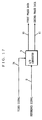
- FIG. 17 is a block diagram showing the structure of the conventional video signal processing device carrying out the two-phase processing in the A/D converter.
- the video signal processing device is an A/D converter 3 receiving a reference signal 9 and a video signal 24 from an image signal source, carrying out the two-phase processing, and outputting first phase data 10 and second phase data 11. Described next below is the operation of such video signal processing device with reference to FIGS. 17 and 18.
- FIG. 18 is a diagram in assistance of explaining the operation of the A/D converter 3 in FIG. 17.
- a to e denote video data included in the video signal 24 in a valid video period.
- Blackened objects in the shape of a circle, diamond, square, and triangle denote data in the pedestal level, specifically black data, in a back porch.
- t1 to t10 each indicate a certain time. Arrows therein schematically show the two-phase processing in the A/D converter 3.
- the video signal 24 includes the back porch and the video data.
- the back porch is between time t1 (or before) and time t5, while the video signal data is included from time t5 and onward. Accordingly, the video signal 24 has such structure that a leading edge of a signal including the video data follows an end of the back porch.
- the digital data both outputted from the A/D converter 3 is determined based on a phase relationship between the digital data and the video signal 24.
- the reference signal 9 is a horizontal synchronizing signal provided from the image signal source.
- the A/D converter 3 starts the two-phase processing at time t1.
- the black data denoted by the blackened circle is outputted from the A/D converter 3 as the first phase data 10.
- the black data denoted by the diamond is outputted from the A/D converter 3 as the second phase data 11.
- the black data each denoted by the square and the triangle is outputted.
- the head data a is outputted from the A/D converter 3 as the first phase data 10.
- the head data a is outputted from the A/D converter 3 as the second phase data 11.
- a display e.g., crystal liquid display and plasma display, on which pixels are fixed in number for display, may cause one dot short when displaying the video data.
- a display e.g., crystal liquid display and plasma display, on which pixels are fixed in number for display, may cause one dot short when displaying the video data.
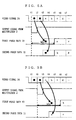
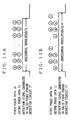
- FIG. 19 is a schematic diagram in assistance of explaining the arrangement of output data and display status on the display for a case where the video data a shown in FIG. 18 is outputted from the A/D converter as the first phase data.
- FIG. 20(a) is a schematic diagram in assistance of explaining the arrangement of output data and display status on the display for a case where the video data a shown in FIG. 18 is outputted from the A/D converter as the second phase data.
- FIG. 20(b) is a schematic diagram in assistance of explaining the case that the data arrangement is the same as in FIG. 20(a), but the display status is different therefrom.
- a to t denote data included in a video signal, from an image signal source, observed on an arbitrary scan line in a valid video period.
- the data inside of a frame in the shape of a square is displayed on the display, while the data outside of the frame is not displayed on the display.
- the display where pixels displayed thereon are fixed in number displays every video data from a to t .
- the display where pixels displayed thereon are fixed in number displays every video data from a to t .
- FIGS. 20(a) and (b) when the head data a is included in the second phase data 11, either the video data t on the right end or the video data a on the left end is problematically not displayed on the display. This is because the digital signal processing device in the stage subsequent to the A/D converter 3 carries out processing in a frequency half of a dot clock coming from the image signal source, causing a video phase on the display to change only in pairs of pixels.
- the conventional video signal processing device when the head data a is included in the second phase data 11, the video data is displayed in a state of one dot short as shown in FIG. 20(a) or (b). Consequently, as shown in FIG. 19, the video data a to t cannot be simultaneously displayed.
- an object of the present invention is to provide a video signal processing device being capable of, even if with an A/D converter carrying out the two-phase processing, displaying every pixel on a display even if a head of video data is not in the first phase output data.
- a first aspect of the present invention is directed to a video signal processing device for displaying, on a display, every pixel in a video signal inputted from an image signal source, the device comprising:
- a display can display every pixel by regarding a signal being delayed by one clock phase.
- correct counting can be achieved by using the number of dot clocks coming from an image signal source.
- a third aspect of the present invention in the first aspect of the present invention, further comprising a first minimum value retention circuit for inputting, into the comparator, a minimum value of the first back porch periods outputted from the first back porch detection circuit as another first back porch period, and
- a fourth aspect of the present invention is directed to a video signal processing device for displaying, on a display, every pixel in a video signal inputted from an image signal source, the device comprising:
- a display can assuredly display every video signal with such structure that a back porch period is stored and outputted in a manner corresponding to each state, and based on data outputted thereby, a comparator carries out its determination operation.
- a detection signal used therein is either first phase data or second phase data outputted from the A/D converter. Therefore, without using both data as the detection signal, the video signal processing device can be reduced in area for wiring on a substrate, for example.
- the back porch detection circuit detects the back porch period by using the number of clocks in the video signal.
- correct counting can be achieved by using the number of dot clocks coming from an image signal source.
- a sixth aspect of the present invention is directed to a video signal processing device for displaying, on a display, every pixel in a video signal inputted from an image signal source, the device comprising:
- a display can assuredly display every video signal with such structure that a comparator receives the number of pixels detected by a valid video period detection circuit where receiving a detection pulse each detected by a leading edge detection circuit and a falling edge detection circuit, and a value half of horizontal resolution from an image signal source connected to the present video signal processing device, and then carries out its determination operation.
- the valid video period detection circuit detects the valid video period by using the number of clocks in the video signal.
- correct counting can be achieved by using the number of dot clocks coming from an image signal source.
- An eighth aspect of the present invention is directed to a video signal processing device for displaying, on a display, every pixel in a video signal inputted from an image signal source, the device comprising:
- a display can assuredly display every video signal with such structure that a comparator receives the number of pixels detected by a valid video period detection circuit where receiving a detection pulse each detected by a leading edge detection circuit and a falling edge detection circuit, and a value half of horizontal resolution from an image signal source connected to the present video signal processing device, and then carries out its determination operation.
- the valid video period detection circuit detects the valid video period by using the number of clocks in the video signal.
- correct counting can be achieved by using the number of dot clocks coming from an image signal source.
- a tenth aspect of the present invention is directed to a video signal processing device for displaying, on a display, every pixel in a video signal inputted from an image signal source, the device comprising:
- a display can assuredly display every video signal with such structure that a valid video period is detected but not a horizontal resolution.
- correct counting can be achieved by using the number of dot clocks coming from an image signal source.
- a twelfth aspect of the present invention is directed to a video signal processing device for displaying, on a display, every pixel in a video signal inputted from an image signal source, the device comprising:
- correct counting can be achieved by using the number of dot clocks coming from an image signal source.
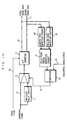
- FIG. 1 is a block diagram showing the structure of a video signal processing device according to a first embodiment of the present invention.
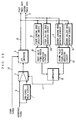
- the present video signal processing device includes a one-clock delay circuit 1 where receiving the reference signal 9 and outputting a one-clock-delayed signal, a multiplexer 2 for receiving the output signal from the one-clock delay circuit 1 and the reference signal 9, the A/D converter 3 where receiving an output signal from the multiplexer 2 and the video signal 24 and carrying out the two-phase processing, first and second leading edge detection circuits 4 and 5 for detecting a leading edge of an output signal from the A/D converter 3, first and second back porch detection circuits 6 and 7 for receiving signals from each corresponding first and second leading edge detection circuits 4 and 5 and the output signal from the multiplexer 2, and a comparator 8 where receiving signals each from the first and second leading edge detection circuits 6 and 7 and outputting a control signal 12 for the multiplexer 2. Described below is the operation of such structured video signal processing device.
- the reference signal 9 provided from an image signal source connected to the present video signal processing device is applied to both the multiplexer 2 and the one-clock delay circuit 1.
- the reference signal 9 is generally a horizontal synchronizing signal from the image signal source, but is not necessarily restricted thereto.
- the one-clock delay circuit 1 delays the received reference signal 9 by one clock for output to the multiplexer 2.
- the one-clock delay circuit 1 delays the reference signal 9 by one dot clock, i.e., one pixel, out of those from the image signal source.
- the multiplexer 2 selects either the received reference signal 9 or an output signal from the one-clock delay circuit 1 for output.
- the multiplexer 2 switches from one received signal which has been selected into the other for output. It is now assumed that the multiplexer 2 has been selecting, for output, the received reference signal 9 but not the output signal from the one-clock delay circuit 1.
- the multiplexer 2 in its switching operation, stops outputting the reference signal 9 which has been selected, and starts outputting the output signal from the one-clock delay circuit 1.
- the multiplexer 2 presumably selects the reference signal 9 for output.
- the output signal from the multiplexer 2 is applied to the A/D converter 3.
- the A/D converter 3 goes through the two-phase processing after receiving the video signal 24 and the output signal from the multiplexer 2.
- the A/D converter 3 subjects the video signal 24 to A/D conversion, and then carries out the two-phase conversion so as to simultaneously output the first phase data 10 and the second phase data 11.
- These digital data is provided to a digital data processing device (not shown) provided in a stage subsequent to the A/D converter 3 for signal processing, and then displayed on a display.
- the digital data outputted from the A/D converter 3, that is, the first phase data 10 and the second phase data 11 is provided to the first and second leading edge detection circuits 4 and 5, respectively.
- the first and second leading edge detection circuits 4 and 5 each detect a leading edge of a valid video signal region in the video signal 24 which has been applied to the A/D converter 3.
- a blanking period coming from a general image signal source being black from the reference signal 9 to the valid video region. That is, the leading edge of the valid video signal region can be easily detected by detecting a period starting from the reference signal 9 till the video signal rises.
- the head data in the valid video signal region when the head data in the valid video signal region is in the pedestal level, the leading edge of the valid video signal region cannot be detected with correctness. In such case, however, the head data in the valid video signal region is always one or more pixels short. Therefore, no such problem occurs that the display where pixels displayed thereon are fixed in number cannot display every data provided from the image signal source connected to the present video signal processing device.
- the first and second leading edge detection circuits 4 and 5 input the leading edge in a form of pulse signal to the first and second back porch detection circuits 6 and 7, respectively.
- the first and second back porch detection circuits 6 and 7 then detect a back porch period between the signal outputted from the multiplexer 2 and the leading edge of the valid video signal region detected by the first and second leading edge detection circuits 4 and 5, respectively.
- the first and second leading edge detection circuits 4 and 5 each include a counter circuit, and count the back porch period by referring to the number of dot clocks from the image signal source. As such, the number of dot clocks from the image signal source helps the first and second leading edge detection circuits 4 and 5 counting in a correct manner.
- the back porch period is thus defined as a period starting from a leading edge of a signal outputted from the multiplexer 2 to a head position of data in a valid video signal region excepting data in the black level.
- the back porch periods detected by the first and second back porch detection circuits 6 and 7 are both provided to the comparator 8.
- the comparator 8 then outputs the control signal 12 based on a result obtained through determination logic, which will be later described.
- the multiplexer 2 switches, for output, between the output signal from the one-clock delay circuit 1 and the reference signal 9. If the comparator 8 decided not to output the control signal 12 in accordance with the result obtained through the determination logic which will be later described, the multiplexer 2 surely does not go through its switching operation.
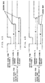
- FIGS. 2 are time charts showing the relationship between the reference signal 9 and the output signals from the first and second leading edge detection circuits 4 and 5. Specifically, FIG. 2(a) shows a case where the head data (data on the left end on the display) in the valid video signal region is outputted from the first phase of the A/D converter 3, while FIG. 2(b) shows a case where the head data is outputted from the second phase of the A/D converter 3.
- the back porch period is a period detected starting from the pulse position of the signal outputted from the multiplexer 2 to the head data in the valid video signal region. It is now assumed that a back porch number is a value obtained by counting the number of dots (the number of clocks) in the back porch period.
- BP1 the back porch number for the output signal from the leading edge detection circuit 4
- BP2 the back porch number for the output signal from the leading edge detection circuit 5
- the head data is included in the first phase data 10. Therefore, for the output signal from the leading edge detection circuit 4 where receiving the first phase data 10, the back porch number BP1 always shows such relationship with the back porch number BP2 as an equation (1) next below.
- the comparator 8 does not output the control signal 12 to the multiplexer 2.
- the multiplexer 2 keep outputting the reference signal 9 without its switching operation.
- the A/D converter 3 becomes possible to retain a state that the head data in the valid video signal region is always outputted from the first phase data. Therefore, once retaining such state that the head data is always outputted from the first phase data, the present video signal processing circuit basically has no need to operate thereafter.
- the head data in the valid video signal region is included in the second phase data 11. Therefore, for the output signal from the leading edge detection circuit 5 where receiving the second phase data 11, the back porch number BP2 always shows such relationship with the back porch number BP1 as an equation (2) next below.
- the comparator 8 When the above equation (2) is satisfied, the comparator 8 outputs the control signal 12 to the multiplexer 2 so as to bring the multiplexer 2 to select the signal from the one-clock delay circuit 1.
- the multiplexer 2 switches its output signal. Specifically, the multiplexer 2 selects the signal from the one-clock delay circuit 1 for output to the A/D converter 3.
- the A/D converter 3 starts regarding a signal whose phase is delayed by one clock as a reference, retaining the state that the bead data in the valid video signal region is always outputted from the first phase data.
- the present video signal processing circuit basically has no need to operate once such state is retained that the head data is always outputted from the first phase data.
- the present video signal processing device can retain the state that the head data in the valid video signal region is always outputted from the first phase data. This is because, the comparator 8 outputs the control signal 12 to the multiplexer 2 through such determination operation described in the foregoing, and thus the multiplexer 2 switches its output signal into the reference signal 9.
- the video signal processing device of this embodiment is capable of displaying every pixel on a display by regarding a signal whose phase is delayed by one clock as a reference.
- the video signal processing device of this embodiment can be in such structure that the first and second leading edge detection circuits 4 and 5 are replaced with first and second falling edge detection circuits, respectively.
- the first and second back porch detection circuits 6 and 7 operate to detect a period including both the back porch period and the valid video signal period. Even with such alternative structure, the video signal processing device of this embodiment can operate in a similar manner.
- the one-clock delay circuit 1 in the present video signal processing device may be a three-clock delay circuit or a five-clock delay circuit. That means, the one-clock delay circuit 1 may be any type of circuit as far as the reference signal 9 is delayed by the odd number of clocks therein. Still further, although an A/D converter described in this embodiment is the one carrying out the two-phase processing, an A/D converter carrying out four-phase processing or six-phase processing can easily operate in a similar manner.
- FIG. 3 is a block diagram showing the structure of a video signal processing device according to a second embodiment of the present invention.
- the present video signal processing device is almost identical in structure to the above-described video signal processing device of the first embodiment.
- the present video signal processing device is not provided with the second leading edge detection circuit 5 and the second back porch detection circuit 7 in FIG. 1.
- the first leading edge detection circuit 4 in FIG. 1 is replaced with a leading edge detection circuit 40, and the first back porch detection circuit 6 with a back porch detection circuit 60, and a storage part 13 is additionally provided.
- any constituent identical to that in the video signal processing device of the first embodiment is under the same reference numeral, and is not described again.
- a comparator 15 is different from the comparator 8 in reference numeral since receiving a signal different from the one thereto.
- the multiplexer 2 selects the reference signal 9 for output to the A/D converter 3 without any change.
- the A/D converter 3 subjects the video signal 24 to A/D conversion and then carries out the two-phase processing so that the video signal 24 is outputted as the first phase data 10 and the second phase data 11.
- the first phase data 10 is provided to the leading edge detection circuit 40.
- the leading edge detection circuit 40 detects a leading edge of a valid video signal region in the video signal 24. A result obtained by the detection is provided to the back porch detection circuit 60.
- the back porch detection circuit 60 detects a back porch period between a leading edge of the signal (herein, the reference signal 9) outputted from the multiplexer 2 and a leading edge of the valid video signal region outputted from the leading edge detection circuit 40.
- the back porch period thus detected is provided to the storage part 13.
- the storage part 13 stores the period, and keeps outputting the period to the comparator 15 at predetermined intervals.
- the comparator 15 When detecting an input only of the period, the comparator 15 outputs the control signal 12 to the multiplexer 2 so as to bring the multiplexer 2 to change its output signal to an output signal from the one-clock delay circuit 1.
- the reason for the comparator 15 carrying out such operation is to have the storage part 13 store the back porch period starting from the leading edge of the reference signal 9, and then have the storage part 13 store also the back porch period starting from the leading edge of the output signal from the one-clock delay circuit 1.
- the multiplexer 2 switches into the output signal from the one-clock delay circuit 1 for output to the A/D converter 3.
- the A/D converter 3 regards the received signal as a reference, and subjects the video signal 24 to A/D conversion then carries out the two-phase conversion.
- the leading edge detection circuit 40 detects the leading edge of the valid video signal region in the video signal 24.
- the back porch detection circuit 60 detects the back porch period in a similar manner to the above. The back porch period thus detected is provided to the storage part 13.
- the storage part 13 then provides both the received back porch period and the stored back porch period to the comparator 15.
- the received back porch period may be once stored into the storage part 13.
- the comparator 8 determines whether or not outputting the control signal 12 again based on a result obtained through determination logic, which will be later described. If the control signal 12 is inputted, the multiplexer 2 switches its output signal between the output signal from the one-clock delay circuit 1 and the reference signal 9.
- FIGS. 4 are time charts showing the relationship between the reference signal 9 and the output signal from the storage part 13. Specifically, FIG. 4(a) shows a case where head data (data on the left end on the display) in the valid video signal region is outputted from the first phase of the A/D converter 3, while FIG. 4(b) shows a case where the head data is outputted from the second phase of the A/D converter 3.
- FIGS. 5 are time charts showing the flow of data for a case where the head data in the valid video signal region is outputted from the first phase of the A/D converter 3. Specifically, FIG. 5(a) shows a case where the reference signal 9 is applied to the A/D converter 3 without being delayed, while FIG. 5(b) shows a case where the reference signal 9 is delayed by one clock before applied to the A/D converter 3.
- FIGS. 6 are time charts showing the flow of data for a case where the head data is outputted from the second phase of the A/D converter 3. Specifically, FIG. 6(a) shows a case where the reference signal 9 is applied to the A/D converter 3 without being delayed, while FIG. 6(b) shows a case where the reference signal 9 is delayed by one clock before applied to the A/D converter 3.
- the back porch number is presumed to be a value obtained by counting the number of dots (the number of clocks) in the back porch period.
- the back porch number in the output signal from the storage part 13 is denoted by M1.
- the back porch number in the output signal from the storage part 13 is denoted by M2.
- the leading edge of the output signal from the leading edge detection circuit 40 comes later by one clock or more compared with the case that the reference signal 9 is inputted to the A/D converter 3 without being delayed.
- the leading edge of the output signal from the leading edge detection circuit 40 comes later only by one clock in the case that the reference signal 9 is delayed only by one clock. If the data is in the black level, the leading edge thereof comes later by more clocks.
- the output signal from the multiplexer 2 is delayed by one clock, the relationship between the back porch numbers M1 and M2 can be expressed by an equation (3) next below.
- FIGS. 5(a) and (b) t1 to t7 each indicate a time
- arrows therein schematically show the two-phase processing in the A/D converter 3.
- blackened circle and square denote data in the black level in the back porch
- a to d denote video data in the valid video signal region.
- the video data a located immediately after the leading edge of the video signal 24 is assumed not in the black level. This is because, if the data is in the black level, such problem to be solved by the present video signal processing device that a display cannot display every data does not occur as described in the foregoing.
- the leading edge of the output signal from the multiplexer 2 is at time t1.
- the A/D converter 3 starts the two-phase processing.
- the A/D converter 3 keeps simultaneously outputting the received data until completely receiving next two data. Accordingly, the A/D converter 3 outputs the data denoted by the blackened circle and square at time t3, and outputs the video data a and b at time t5.
- the first phase data 10 goes to the leading edge detection circuit 40.
- the leading edge of the output signal from the leading edge detection circuit 40 is found at time t5, and it is known that the back porch number M1 between times t1 and t5 is 4. Note herein that, since the video data a is not in the black level, M1 is determined regardless of the arrangement of the video data.
- the A/D converter 3 starts the two-phase processing in response to the video signal 24 inputted at time t2, outputs the data denoted by the blackened square and the video data a at time t4, and outputs the video data b and c at time t6.
- the video signal processing device of this embodiment only the first phase data 10 goes to the leading edge detection circuit 40.
- the leading edge of the output signal from the leading edge detection circuit 40 is found at time t6. It is thus known that the back porch number M2 between times t2 and t6 is 4.
- the video data b or data following thereto may be in the black level. If this is the case, the leading edge of the output signal from the leading edge detection circuit 40 will be found later than time t6. Accordingly, M2 becomes 4 or larger and never fails to be equal to or larger than M1 in value. Therefore, the relationship such as the above equation (3) is thus satisfied.
- FIGS. 6(a) and (b) t1 to t8 each denote a time
- arrows therein schematically show the two-phase processing in the A/D converter 3.
- the blackened circle, square, and triangle indicate the data in the black level in the back porch
- a to d indicate the video data in the valid video signal region.
- the video data a immediately after the leading edge of the video signal 24 is not in the black level.
- the leading edge of the output signal from the multiplexer 2 is at time t1.
- the A/D converter 3 starts the two-phase processing. Thereafter, at time t3, the A/D converter 3 outputs data denoted by the blackened circle and square, at time t5, outputs data denoted by the blackened triangle and the video data a , and at time t7, outputs the video data b and c .
- the video signal processing device of the present invention only the first phase data 10 goes to the leading edge detection circuit 40.
- the leading edge of the output signal from the leading edge detection circuit 40 is found at time t7, and it is known that the back porch number M1 between times t1 and t7 is 6.
- the video data b or the video data b with the data following thereto may be in the black level. In such case, the leading edge of the output signal from the leading edge detection circuit 40 will be found later than time t7.
- the leading edge of the output signal from the multiplexer 2 is at time t2.
- the A/D converter 3 starts the two-phase processing, outputs data denoted by the blackened square and triangle at time t4, and outputs the video data a and b at time t6. Since only the first phase data 10 goes to the leading edge detection circuit 40 in the video signal processing device of this embodiment, the leading edge of the output signal from the leading edge detection circuit 40 is found at time t6. It is thus known that the back porch number M2 between times t2 and t6 is 4, and rendering M2 always smaller than M1 in value. As such, such relationship as the above equation (4) is established.
- the comparator 8 again outputs the control signal 12 to the multiplexer 2.
- the multiplexer 2 again goes through its switching operation so as to output the reference signal 9.
- the A/D convertor 3 can retains a state that the head data in the valid video signal region is outputted always from the first phase data. Therefore, similarly in the first embodiment, the present video signal processing circuit basically has no need to operate once such state that the head data is outputted always from the first phase data is retained.
- the comparator 8 does not output the control signal 12 to the multiplexer 2 so as to let the multiplexer 2 keep selecting the signal from the one-clock delay circuit 1.
- the multiplexer 2 keeps selecting the signal from the one-clock delay circuit 1 for output to the A/D converter 3.
- the A/D converter 3 regards a signal whose phase is delayed by one clock as a reference, and thus, the head data in the valid video signal region is assured to be always outputted from the first phase data.
- the present video signal processing circuit has no need to operate once such state that the head data is always outputted from the first phase data is retained.
- the present video signal processing device can retain the state that the head data in the valid video signal region is always outputted from the first phase data.
- a display can assuredly display every video signal thereon.
- the video signal processing device of this embodiment does not use the second phase data 11 outputted from the A/D converter 3 as a detection signal. Therefore, in the present video signal processing device, wiring on a substrate can be reduced in area, for example.
- the video signal processing device of this embodiment can be provided with a falling edge detection circuit instead of the leading edge detection circuit 40. If this is the case, the back porch detection circuit 60 operates to detect a period including both the back porch period and the valid video signal period. In such alternative structure, the video signal processing device of this embodiment can operate in a similar manner.
- the one-clock delay circuit 1 may be any type of circuit as far as the reference signal 9 is delayed by the odd number of clocks therein.
- the A/D converter 3 may be the one carrying out four-phase processing or six-phase processing, which can easily operate in a similar manner.
- FIG. 7 is a block diagram showing the structure of a video signal processing device according to a third embodiment of the present invention.
- the present video signal processing device is almost identical in structure to the above-described video signal processing device of the second embodiment in FIG. 3.
- the present video signal processing device is not provided with the back porch detection circuit 60 and the storage part 13 in FIG. 3, but is newly provided with a falling edge detection circuit 16 and a valid video signal period detection circuit 17.
- a comparator 18 is different from the comparator 15 in reference numeral since receiving a signal different from the one thereto. Described next below is the operation of such structured present video signal processing device with reference to FIGS. 8 and 9.
- the leading edge detection circuit 40 detects a position where the first phase data 10 first rises with reference to a pulse of an output signal from the multiplexer 2. A result obtained by the detection is outputted In a form of pulse signal as shown in FIG. 8.
- the falling edge detection circuit 16 detects a position where the second phase data 11 falls last with reference to a pulse position of the output signal from the multiplexer 2. The result obtained thereby is outputted in such form of pulse signal as shown in FIG. 8.
- the signals outputted from the leading edge detection circuit 40 and the falling edge detection circuit 16 go to the valid video signal period detection circuit 17. From those signals, the valid video signal period detection circuit 17 generates a valid video signal detection signal therein as shown in FIG. 8. Moreover, the valid video signal period detection circuit 17 includes a counter circuit, and counts the above valid video period detection signal for pulse width on the basis of the number of dot clocks from the image signal source, and detects the number of pixels included in the valid video signal processing period. As such, the number of dot clocks from the image signal source helps the valid video period detection circuit 17 counting in a correct manner. Note herein that, by the two-phase processing carried out In the A/D converter 3, the number of pixels is reduced to half of that in the valid video period for the actual video signal 24.
- the comparator 18 receives the number of pixels included in the valid video signal period detected by the valid video period detection circuit 17.
- the comparator 18 also receives, from a value output part which is not shown, a value half of the horizontal resolution in the image signal source connected to the present video signal processing device.
- the horizontal resolution in the image signal source can be easily calculated from frequencies of a horizontal synchronizing signal and a vertical synchronizing signal unique to the image signal source.
- the comparator 18 Based on a result obtained by subjecting each received value to a predetermined determination logic, the comparator 18 outputs the control signal 12 to the multiplexer 2.
- the multiplexer 2 switches its output signal between the output signal from the one-clock delay circuit 1 and the reference signal 9.
- the comparator 8 decided not to output the control signal 12 according to the result obtained by the determination logic which will be later described, the multiplexer 2 surely does not go through its switching operation.
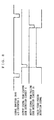
- FIGS. 9 are time charts showing the relationship among the detection signal generated in the valid video period detection circuit 17, the first phase data 10, and the second phase data 11. Specifically, FIG. 9(a) shows a case where head data (data on the left end on the display) in the valid video signal region is outputted from the first phase of the A/D converter 3, while FIG. 9(b) shows a case where the head data is outputted from the second phase of the A/D converter 3.
- a to t denote data included in the video signal 24 provided to the A/D converter 3.
- each of a to t is assumed to be ON.
- the data included in the video signal 24 may be in the black level.
- head data (data on the left end on the display) a in the valid video signal region is included in the first phase data 10.
- the data b which is the second from the head is included in the second phase data 11 at the same phase position as a in the first phase data.
- the A/D converter 3 subjects 20 pieces of data from data a to data t to the two-phase processing.
- the comparator 8 does not output the control signal 12 to the multiplexer 2.
- the multiplexer 2 thus outputs the reference signal 9 without going through its switching operation.
- the A/D converter 3 can retain such state that the head data in the valid video signal region is outputted always from the first phase data. Accordingly, similarly to the case in the first embodiment, the present video signal processing circuit basically has no need to operate once such state that the head data is always outputted from the first phase data is retained.
- the head data (data on the left end of the display) a in the valid video signal region is included in the second phase data 11.
- the data b second from the head is included in the second phase data 11 at a position having the one-clock-delayed phase relationship with the position of a in the first phase data.
- the A/D converter 3 subjects 20 pieces of data from data a to data t to the two-phase processing.
- the comparator 8 When the above-equation (6) is satisfied, the comparator 8 outputs the control signal 12 to the multiplexer 2 so as to bring the multiplexer 2 to select a signal from the one-clock delay circuit 1.
- the multiplexer 2 switches its output signal.
- the multiplexer 2 selects a signal from the one-clock delay circuit 1 for output to the A/D converter 3.
- the A/D converter 3 regards a one-clock-delayed signal as a reference, retaining the state that the head data in the valid video signal region is always outputted from the first phase data. Therefore, similar to the case in the first embodiment, the present video signal processing circuit basically has no need to operate once the state that the head data is always outputted from the first phase data is retained.
- the present video signal processing device can retain the state that the head data in the valid video signal region is always outputted from the first phase data.
- the valid video period detection circuit 17 where receiving pulses detected by the leading edge detection circuit 40 and the falling edge detection circuit 16 detects the number of pixels in the valid video period
- the comparator 18 receives the number of pixels and a value half of the horizontal resolution for comparison
- each of the video data a to t in the valid video signal region in the video signal 24 is assumed to be ON in this embodiment, the present video signal processing device operates in a similar manner to the above if only the data a and t is ON.
- the one-clock delay circuit 1 may be any type of circuit as far as the reference signal 9 is delayed by the odd number of clocks therein.
- the A/D converter 3 may be the one carrying out four-phase processing or six-phase processing, which can easily operate in a similar manner.
- FIG. 10 is a block diagram showing the structure of a video signal processing device according to a fourth embodiment of the present invention.
- the present video signal processing device is almost identical in structure to the above-described video signal processing device of the third embodiment in FIG. 7.
- constituents in the present video signal processing device are the same as those in the video signal processing device of the third embodiment, and thus are under the same reference numerals and not described again.
- the leading edge detection circuit 40 receives the first phase data 10 and the falling edge detection circuit 16 receives the second phase data 11, but in the present video signal processing device, the leading edge detection circuit 40 receives the second phase data 11 and the falling edge detection circuit 16 receives the first phase data 10. Described below is the reason for such differences.
- the valid video signal in the video signal 24 provided to the A/D converter 3 needs to be risen at both ends (i.e., the data needs to be ON).
- the detection signal generated in the valid video period detection circuit 17 is less than a half of the horizontal resolution in the image signal source.
- the comparator 18 outputs the control signal 12 so as to bring the multiplexer 2 to switch its outputs.
- the comparator 18 again outputs the control signal 12 so as to bring the multiplexer 2 to switch its output. Consequently, the comparator 18 falls into an endless loop in operation.
- the video signal 24 needs to be conditionally restricted to be ON at both ends. If not conditionally restricted, the video signal processing device needs to be additionally provided with a constituent to detect whether the comparator 18 falls into the above-described endless loop, rendering the circuit complicated and the cost increased.
- FIGS. 11 are time charts showing the relationship among the detection signal generated in the valid video period detection circuit 17, the first phase data 10, and the second phase data 11. Specifically, FIG. 11(a) shows a case where the head data (data displayed on the left end on the display) in the valid video signal region is included in the first phase data 10 from the A/D converter 3, while FIG. 11(b) shows a case where the head data is included in the second phase data from the A/D converter 3.
- a to t denote the data included in the video signal 24 provided to the A/D converter 3.
- each of the data a to t is assumed to be ON.
- the case that the video signal 24 includes data in the black level will be described later.
- the head data (data displayed on the led end on the display) a in the valid video signal region is included in the first phase data 10. Therefore, the data b second from the head is included in the second phase data 11 at the same phase position as the first phase data a .
- the A/D converter 3 subjects 20 pieces of data from data a to data t to the two-phase processing.
- the comparator 8 When the above equation (7) is satisfied, the comparator 8 outputs the control signal 12 to the multiplexer 2 so as to bring the multiplexer 2 to select the reference signal 9.
- the multiplexer 2 selects the reference signal 9 corresponding to the control signal for output to the A/D converter 3.
- the A/D converter 3 can retain a state that the head data in the valid video signal region is always outputted from the first phase data. Therefore, once retaining the state that the head data is always outputted from the first phase data, similar to the case in the first embodiment, the present video signal processing circuit basically has no need to operate thereafter.
- the head data (data displayed on the left end on the display) a in the valid video signal region is included in the second phase data 11. Accordingly, the data b second from the head is included in the second phase data 11 at a position 11 having the one-clock-delayed phase relationship with the position of a in the first phase data.
- the A/D converter 3 subjects 20 pieces of data from data a to data t to the two-phase processing.
- the comparator 8 When the above equation (9) is satisfied, the comparator 8 outputs the control signal 12 to the multiplexer 2 so as to bring the multiplexer 2 to select the signal from the one-clock delay circuit 1. In response to the control signal 12, the multiplexer 2 switches its output signal. Once the signal from the one-clock delay circuit was selected, the A/D converter 3 starts regarding a signal whose phase is delayed by one clock as a reference, retaining a state that the head data in the valid video signal region is always outputted from the first phase data. Therefore, once retaining the state that the head data is always outputted from the first phase data, similar to the case in the first embodiment, the present video signal processing circuit basically has no need to operate thereafter.
- the present video signal processing device can retain the state that the head data in the valid video signal region is always outputted from the first phase data.
- a state that the video signal 24 is always one pixel short on the display is observed only when the above equation (9) is satisfied. This is because, such pixel shortage is not observed when the head or the last of the video data is in the black level, but the video data needs to be ON at both ends in order to satisfy the equation (9).
- the comparator 8 retains the output state from the multiplexer 2 for output to the A/D converter without any change. Detected Number of Pixels ⁇ Horizontal Resolution/2
- the comparator 8 When the above-described equation (9) is satisfied, the comparator 8 outputs the control signal 12 so as to switch the output from the multiplexer 2. With such operation of the comparator 8, the present video signal processing device can bring the display to display a video without pixel shortage.
- the valid video period detection circuit 17 where receiving detection pulses detected by the leading edge detection circuit 40 and the falling edge detection circuit 16 detects the number of pixels
- the comparator 18 receives the detected number of pixels and a value half of the horizontal resolution for comparison
- the one-clock delay circuit 1 may be any type of circuit as far as the reference signal 9 is delayed by the odd number of clocks therein.
- the A/D converter 3 may be the one carrying out four-phase processing or six-phase processing, which can easily operate in a similar manner.
- FIG. 12 is a block diagram showing the structure of a video signal processing device according to a fifth embodiment of the present invention.
- the present video signal processing device is almost identical in structure to the above-described video signal processing device of the third embodiment in FIG. 7.
- the present video signal processing device is provided with a first leading edge detection circuit 4, a first falling edge detection circuit 160, and a first valid video period detection circuit 20 instead of the leading edge detection circuit 40, the falling edge detection circuit 160, and the valid video period detection circuit 17 in FIG. 7.
- a second leading edge detection circuit 5, a second falling edge detection circuit 21, and a second valid video period detection circuit 22 are additionally provided.
- any constituent identical to that in the video signal processing device of the third embodiment is under the same reference numeral, and is not described again.
- a comparator 23 is different from the comparator 15 in reference numeral since receiving a signal different from the one thereto.
- the present video signal processing device may be a combination, in structure, of the video signal processing device of the above-described third embodiment in FIG. 7 and the video signal processing device of the above-described fourth embodiment in FIG. 10. Details are described below.
- the video signal processing devices of the third and fourth embodiments have to detect the horizontal resolution in the image signal source.
- This horizontal resolution in the image signal source can be estimated by detecting, generally, the frequencies of the horizontal synchronizing signal and the vertical synchronizing signal from the respective image signal sources. In the recent market, however, such estimation of the horizontal resolution in the frequencies of the horizontal synchronizing signal and the vertical synchronizing signal may not be applicable to some image signal sources.
- the device needs to be differently structured so as to recognize such image signal sources. Moreover, if such image signal sources vary in type, the device thus differently-structured becomes larger in size, enlarging the circuit in its entirety.
- the video signal processing device of this embodiment can easily clear the above-described problems with the structure as shown in FIG. 12. Next below, the operation of the present video signal processing device is described by referring to FIGS. 13.
- FIGS. 13 are time charts showing the relationship among the detection signals generated in the valid video period detection circuits 17 and 22, the first phase data 10, and the second phase data 11. Specifically, FIG. 13(a) shows a case where the head data (data on the left end on the display) in the valid video signal region is included in the first phase of the A/D converter 3, while FIG. 13(b) shows a case where the head data is included in the second phase of the A/D converter 3.
- a to t denote data included in the video signal 24 provided to the A/D converter 3.
- each of a to t is assumed to be ON.
- the head data (data on the left end on the display) a in the valid video signal region is included in the first phase data 10.
- the data b which is the second from the head is included in the second phase data 11 at the same phase position as a in the first phase data.
- the A/D converter 3 subjects 20 pieces of data from data a to data t to the two-phase processing.
- the leading edge and falling edge of the detection signal generated in the valid video period detection circuit 17 coincide with the leading edge of the first phase data 10 and the falling edge of the second phase data 11, respectively.
- the leading edge and falling edge of the detection signal generated in the valid video period detection circuit 22 coincide with the leading edge of the second phase data 11 and the falling edge of the first phase data 10, respectively.
- This is the same operation as the video signal processing device of the fourth embodiment that is, the same as the above-described case shown in FIG. 11(a).
- the comparator 8 When the above equation (11) is satisfied, the comparator 8 outputs the control signal 12 to the multiplexer 2 so as to bring the multiplexer 2 to select the reference signal 9.
- the multiplexer 2 selects the reference signal 9 corresponding to the control signal for output to the A/D converter 3.
- the A/D converter 3 can retain a state that the head data in the valid video signal region is always outputted from the first phase data. Therefore, once retaining the state that the head data is always outputted from the first phase data, the present video signal processing circuit basically has no need to operate thereafter.
- the head data (data on the left end of the display) a in the valid video signal region is included in the second phase data 11.
- the data b second from the head is included in the second phase data 11 at a position having the one-clock-delayed phase relationship with the position of a in the first phase data.
- the A/D converter 3 subjects 20 pieces of data from data a to data t to the two-phase processing.
- the leading edge and falling edge of the detection signal generated in the valid video period detection circuit 17 coincide with the leading edge of the first phase data 10 and the falling edge of the second phase data 11, respectively.
- the leading edge and falling edge of the detection signal generated in the valid video period detection circuit 22 coincide with the leading edge of the second phase data 11 and the falling edge of the first phase data 10, respectively.
- This is the same operation as the video signal processing device of the fourth embodiment that is, the same as the above-described case shown in FIG. 8(b).
- the comparator 8 When the above equation (12) is satisfied, the comparator 8 outputs the control signal 12 to the multiplexer 2 so as to let the multiplexer 2 select the signal from the one-clock delay circuit 1. In response to the control signal 12, the multiplexer 2 switches its output signal. To be specific, the multiplexer 2 selects the signal from the one-clock delay circuit 1 for output to the multiplexer 2. Once the signal from the one-clock delay circuit 1 was selected, the A/D converter 3 regards a signal whose phase is delayed by one clock as a reference, and thus, such state that the head data in the valid video signal region is always outputted from the first phase data can be retained. As such, similarly to the case in the first embodiment, the present video signal processing circuit has no need to operate once such state that the head data is always outputted from the first phase data is retained.
- the present video signal processing device can retain the state that the head data in the valid video signal region is always outputted from the first phase data.
- FIG. 11(a) described is a case where only the video data a and t is OFF.
- the head data is not included in the first phase data 10
- the last data of the video data is not included in the second phase data 11. That is in the same state as in FIG. 11(b).
- the comparator 8 thus outputs the control signal 12 to the multiplexer 2 so as to bring the multiplexer 2 to select the signal from the one-clock delay circuit 1.
- the multiplexer 2 switches its output signal.
- the multiplexer 2 selects the signal from the one-clock delay circuit 1 for output to the A/D converter 3.
- the A/D converter 3 regards a signal whose phase is delayed by one clock as a reference, and thus, the state that the head data in the valid video signal region is always outputted from the first phase data.
- the head data a in the video signal 24 is included in the second phase data 11. This may sound that the status is not ideal. However, since the video data a and t is the black data, the data has pixel shortage from the beginning, and thus does not cause such problem as described in the foregoing if shown on the display as it is. In FIG. 11(b), when only the video data a and t is OFF, the similar description is applicable.
- FIG. 11(a) it is described a case where any arbitrary pixel excepting for the video data a and t is OFF.
- PW1 becomes larger than PW2.
- the comparator 8 retains the output state of the multiplexer 2, and outputs the same to the multiplexer 2 as it is. PW1 ⁇ PW2
- the comparator 8 does not output the control signal 12 to the multiplexer 12 so that the state for the output signal in the multiplexer 2 is retained.
- the comparator 8 outputs the control signal 12 to the multiplexer 2 so as to bring the multiplexer 2 to switch its output signal.
- the one-clock delay circuit 1 may be any type of circuit as far as the reference signal 9 is delayed by the odd number of clocks therein.
- the A/D converter 3 may be the one carrying out four-phase processing or six-phase processing, resulting in the similar operation.
- the display can assuredly display every video signal thereon without detecting the horizontal resolution in the image signal source.
- FIG. 14 is a block diagram showing the structure of a video signal processing device according to a sixth embodiment of the present invention.
- the present video signal processing device is almost identical in structure to the above-described video signal processing device of the first embodiment in FIG. 1.
- the present video signal processing device is not provided with the multiplexer 2 and the one-clock delay circuit 1, but is newly provided with multiplexers 26 and 27, and a one-clock delay circuit 25. Further, signal input/output is different therein.
- signal input/output is different therein.
- the present video signal processing device is characterized in the position of the one-clock delay circuit 25. Next below, the reason for such characteristic is described.
- the phase of the pulse outputted from the multiplexer 2 is changed in response to the video signal 24 so that the display can assuredly display every video signal thereon.
- the one-clock delay circuit 1 provided in those video signal processing devices delays a signal from an image signal source only by one pixel. Accordingly, when dealing with an image signal source whose resolution is in super high level, the one-clock delay circuit 1 needs to be structured by very high speed elements. If this is the case, problematically, the cost thereof is increased, and the consumption electricity is also increased.
- the present video signal processing device is so structured as shown In FIG. 14 to easily clear the above problems.
- the one-clock delay circuit 25 receives the second phase data 11, and then delays the data by one clock through the two-phase processing (that is, originally two clocks from the image signal source). Accordingly, the one-clock delay circuit 25 can deal with the image signal source having the super high resolution without being structured by the super fast elements.
- the multiplexer 26 receives the first phase data 10, and a signal outputted from the one-clock delay circuit 25 where receiving the second phase data 11, that is, the one-clock delayed second phase data 11.
- the multiplexer 27 receives the first phase data 10 and the second phase data 11.
- the multiplexer 26 selects the first phase data 10 for output, while the multiplexer 26 selects the second phase data 11 for output.
- the multiplexer 26 switches itself to select the one-clock-delayed second phase data 11 for output, while the multiplexer 26 switches itself to select the first phase data 10 for output.
- FIGS. 15 are schematic diagrams showing the relationship among the first phase data 10, the second phase data 11, an output signal 28 from the multiplexer 26, and an output signal 29 from the multiplexer 27.
- a to t denote data included in the video signal 24 going to the A/D converter 3.
- FIG. 15(a) shows a case where the head data (data displayed on the left end on the display) in the valid video signal region is included in the first phase data 10 from the A/D converter 3, while FIG. 15(b) shows a case where the head data is included in the second phase data 11 from the A/D converter 11.
- the comparator 8 operates in a similar manner to the video signal processing device of the first embodiment. That is, as described in the foregoing, when the above equation (1) is satisfied, the comparator 8 does not output the control signal 12 to the multiplexers. Accordingly, as described in the foregoing, the multiplexers 26 and 27 select, without going through its switching operation, the first phase data 10 and the second phase data 11 outputted from the A/D converter 3, respectively, for output. In this manner, the present video signal processing device can retain the state that the head data in the valid video signal region is always outputted from the first phase data. Therefore, once retaining the state that the head data is always outputted from the first phase data, the present video signal processing circuit basically has no need to operate thereafter.
- the comparator 8 operates in the same manner as the video signal processing device of the first embodiment.
- the comparator 8 outputs the control signal 12 to the multiplexers.
- the multiplexers 25 and 26 going through the above-described switching operation.
- the multiplexer 26 switches itself to select the one-clock delayed second phase data 11 for output, while the multiplexer 26 switches itself to select the first phase data 10 for output.
- the present video signal processing device can retain the state that the head data in the valid video signal region is always outputted from the first phase data. Therefore, once retaining the state that the head data is always outputted from the first phase data, the present video signal processing circuit basically has no need to operate thereafter.
- the present video signal processing device can retain the state that the head data in the valid video signal region is always outputted from the first phase data.
- the video signal processing device of this embodiment can deal with an image signal source having higher resolution, and can assuredly let the display display every video signal thereon.
- the video signal processing device of this embodiment can be provided with first and second falling edge detection circuits instead of the first and second leading edge detection circuits 4 and 5.
- the first and second back porch detection circuits 6 and 7 operate to detect a period including the back porch period and the valid video signal period.
- the video signal processing device of this embodiment can also operate in a similar manner.
- the video signal processing device of this embodiment is a modification in structure of the video signal processing device of the first embodiment.
- the video signal processing device of this embodiment can be a modification of the video signal processing device of the above-described second or the fifth embodiment.
- the control signal 12 controlling the multiplexer 2 provided in the video signal processing device of the above-described second or the fifth embodiment can be used as a control signal controlling the multiplexers 26 and 27 provided in the present video signal processing device.
- the video signal processing device of this embodiment can be easily realized by modifying the video signal processing device of the second or the fifth embodiment.
- the one-clock delay circuit 1 may be any type of circuit as far as the reference signal 9 is delayed by the odd number of clocks therein.
- the A/D converter 3 may be the one carrying out four-phase processing or six-phase processing, resulting in a similar operation.
- FIG. 16 is a block diagram showing the structure of a video signal processing device according to a seventh embodiment of the present invention.
- the present video signal processing device is almost identical in structure to the above-described video signal processing device of the first embodiment in FIG. 1.
- the present video signal processing device is newly provided with first and second minimum value retention circuits 30 and 31, and this is the difference from the above-described video signal processing device of the first embodiment.
- any constituent identical to that in the video signal processing device of the first embodiment is under the same reference numeral, and is not described again. Next below, it is described the reason why the first and second minimum value retention circuits 30 and 31 are newly provided.
- the video signal processing device of the first embodiment is so structured that the back porch periods each outputted from the first and second back porch detection circuits 6 and 7 go to the comparator 8, and accordingly let the display display every video signal thereon.
- the back porch period does not stay the same.
- the phase of the line on the image is frequently shifted. In this respect, the video signal processing device does not operate in a normal manner.
- the video signal processing device of this embodiment can clear easily the above-described problem by using, as shown in FIG. 16, the first minimum value retention circuit 30 for receiving the back porch period detected by the first back porch detection circuit 6, and detecting the minimum value thereof, and the second minimum value retention circuit 31 for receiving the back porch period detected by the second back porch detection circuit 7, and detecting the minimum value thereof.
- the operation of the present video signal processing device is described by referring to FIG. 16.
- the first and second minimum value retention circuits 30 and 31 are circuits for detecting, respectively, the minimum value of the back porch periods successively outputted from the corresponding back porch detection circuits 5 and 7.
- the first and second minimum value retention circuits 30 and 31 typically store the minimum value, compare the received back porch period with the minimum value in storage, and operate to update the minimum value.
- the present video signal processing device can fixedly recognize the back porch period of the video signal 24 by utilizing the minimum value thereof. In such manner, the present video signal processing device can operate in a stable manner for detection in the moving images. Further, with the first and second minimum value retention circuits 30 and 31, detection of the back porch period can be carried out real time. Thus, the present video signal processing device can let the display display every pixel of the video signal 24 thereon regardless of the types of the video signal 24 provided from the image signal source.
- the video signal processing device of this embodiment can deal with the case, with ease, that a video signal from the image signal source is a moving image, and can assuredly let the display display every video signal thereon.
- the video signal processing device of this embodiment is provided with the first and second minimum value retention circuits 30 and 31 in addition to the video signal processing device of the first embodiment.
- the video signal processing device of this embodiment may be provided with first and second maximum value retention circuits instead of the first and second minimum value retention circuits 30 and 31, and the first and second falling edge detection circuits instead of the first and second leading edge detection circuits 4 and 5.
- the first and second back porch detection circuits 6 and 7 operate to detect a period including both the back porch period and the valid video signal period.
- the video signal processing device of this embodiment can operate in a similar manner.
- the one-clock delay circuit 25 may be any type of circuit as far as the reference signal 9 is delayed by the odd number of clocks therein.
- the A/D converter 3 may be the one carrying out four-phase processing or six-phase processing, resulting in the same operation.
- a display on which pixels are fixed in number for display can display every video signal from an image signal source connected to a video signal processing device by detecting a back porch period or a valid video signal period in data varied in phase outputted from an A/D converter, and even if the image signal source is higher in resolution, the display can assuredly display every video signal by switching output data varied in phase from the A/D converter.
Landscapes
- Engineering & Computer Science (AREA)
- Physics & Mathematics (AREA)
- Computer Hardware Design (AREA)
- General Physics & Mathematics (AREA)
- Theoretical Computer Science (AREA)
- Liquid Crystal Display Device Control (AREA)
- Control Of Indicators Other Than Cathode Ray Tubes (AREA)
- Transforming Electric Information Into Light Information (AREA)
Abstract
Description
Claims (13)
- A video signal processing device for displaying, on a display, every pixel in a video signal inputted from an image signal source, the device comprising:a clock delay circuit for receiving a reference signal, and delays the reference signal by the odd number of clocks for output:a multiplexer for selecting either said reference signal or an output signal from said clock delay circuit for output;an A/D converter for converting said video signal into a digital signal for two-phase output as first phase data and second phase data with reference to an output signal from said multiplexer;a first leading edge detection circuit for detecting a leading edge of a valid video signal region in said first phase data, and outputs a detection signal corresponding thereto;a second leading edge detection circuit for detecting a leading edge of a valid video signal region in said second phase data, and outputs a detection signal corresponding thereto;a first back porch detection circuit for detecting a first back porch period starting from the output signal from said multiplexer to the detection signal outputted from said first leading edge detection circuit;a second back porch detection circuit for detecting a second back porch period starting from the output signal from said multiplexer to the detection signal outputted from said second leading edge detection circuit; anda comparator for comparing said first back porch period and said second back porch period, and when said first back porch period is longer than said second back porch period, determining that head data in the valid video signal region in said video signal is not included in said first phase data, and outputting a signal for controlling said multiplexer to switch an output signal therefrom.
- The video signal processing device according to claim 1, wherein said first back porch detection circuit detects said first back porch period by using the number of clocks in said video signal, andsaid second back porch detection circuit detects said second back porch period by using the number of clocks in said video signal.
- The video signal processing device according to claim 1, further comprising a first minimum value retention circuit for inputting, into the comparator, a minimum value of said first back porch periods outputted from said first back porch detection circuit as another first back porch period, anda second minimum value retention circuit for inputting, into the comparator, a minimum value of said second back porch period outputted from said second back porch detection circuit as another second back porch period.
- A video signal processing device for displaying, on a display, every pixel in a video signal inputted from an image signal source, the device comprising:a clock delay circuit for receiving a reference signal, and delays the reference signal by the odd number of clocks for output;a multiplexer for selecting either said reference signal or an output signal from said clock delay circuit for output;an A/D converter for converting said video signal into a digital signal for two-phase output as first phase data and second phase data with reference to an output signal from said multiplexer;a leading edge detection circuit for detecting, in a predetermined manner, a leading edge of a valid video signal region in either predetermined said first phase data or said second phase data, and outputs a detection signal corresponding thereto;a back porch detection circuit for detecting a back porch period starting from the output signal from said multiplexer to the detection signal outputted from said leading edge detection circuit;a storage part for receiving said back porch period, and storing and outputting in a manner each corresponding to said reference signal selected and outputted by said multiplexer and the output signal from said clock delay circuit; anda comparator for outputting a control signal for controlling said multiplexer to switch a signal selected and outputted therefrom so that said storage part outputs a back porch period each corresponding to the signal selected and outputted from said multiplexer, comparing the corresponding back porch periods outputted from said storage part with each other, and when the back porch period corresponding to said reference signal is equal to or shorter than the back porch period corresponding to the output signal from said clock delay circuit, determining that head data in the valid video signal region in said video signal is included in said first phase data, and outputting said control signal again.
- The video signal processing device according to claim 4, wherein said back porch detection circuit detects said back porch period by using the number of clocks in said video signal.
- A video signal processing device for displaying, on a display, every pixel in a video signal inputted from an image signal source, the device comprising:a clock delay circuit for receiving a reference signal, and delays the reference signal by the odd number of clocks for output;a multiplexer for selecting either said reference signal or an output signal from said clock delay circuit for output;an A/D converter for converting said video signal into a digital signal for two-phase output as first phase data and second phase data with reference to an output signal from said multiplexer;a leading edge detection circuit for detecting a leading edge of a valid video signal region in said first phase data, and outputs a detection signal corresponding thereto;a falling edge detection circuit for detecting a falling edge of a valid video signal region in said second phase data, and outputting a detection signal corresponding thereto;a valid video period detection circuit for detecting a valid video period starting from the detection signal outputted from said leading edge detection circuit to the detection signal outputted from said falling edge detection circuit; anda comparator for comparing a value half of an inputted horizontal resolution with said valid video period, and when the value half of said horizontal resolution is larger than said valid video period in value, determining that head data in the valid video signal region in said video signal is not included in said first phase data, and outputting a signal for controlling said multiplexer to switch an output signal therefrom.
- The video signal processing device according to claim 6, wherein said valid video period detection circuit detects said valid video period by using the number of clocks in said video signal.
- A video signal processing device for displaying, on a display, every pixel in a video signal inputted from an image signal source, the device comprising:a clock delay circuit for receiving a reference signal, and delays the reference signal by the odd number of clocks for output;a multiplexer for selecting either said reference signal or an output signal from said clock delay circuit for output;an A/D converter for converting said video signal into a digital signal for two-phase output as first phase data and second phase data with reference to an output signal from said multiplexer;a leading edge detection circuit for detecting a leading edge of a valid video signal region in said second phase data, and outputs a detection signal corresponding thereto;a falling edge detection circuit for detecting a falling edge of the valid video signal region in said first phase data, and outputs a detection signal corresponding thereto;a valid video period detection circuit for detecting a valid video period starting from the detection signal outputted from said leading edge detection circuit to the detection signal outputted from said falling edge detection circuit; anda comparator for comparing a value half of an inputted horizontal resolution with said valid video period, and when the value half of said horizontal resolution is smaller than said valid video period in value, determining that head data in the valid video signal region in said video signal is not included in said first phase data, and outputting a signal for controlling said multiplexer to switch an output signal therefrom.
- The video signal processing device according to claim 8, wherein said valid video period detection circuit detects said valid video period by using the number of clocks in said video signal.
- A video signal processing device for displaying, on a display, every pixel in a video signal inputted from an image signal source, the device comprising:a clock delay circuit for receiving a reference signal, and delays the reference signal by the odd number of clocks for output;a multiplexer for selecting either said reference signal or an output signal from said clock delay circuit for output;an A/D converter for converting said video signal into a digital signal for two-phase output as first phase data and second phase data with reference to an output signal from said multiplexer;a first leading edge detection circuit for detecting a leading edge of a valid video signal region in said first phase data, and outputs a detection signal corresponding thereto;a second leading edge detection circuit for detecting a leading edge of a valid video signal region in said second phase data, and outputs a detection signal corresponding thereto;a first falling edge detection circuit for detecting a falling edge of the valid video signal region in said second phase data, and outputs a detection signal corresponding thereto;a second falling edge detection signal for detecting a falling edge of the valid video signal region in said first phase data, and outputs a detection signal corresponding thereto;a first valid video period detection circuit for detecting a first valid video period starting from the detection signal outputted from said first leading edge detection circuit to the detection signal outputted from said first falling edge detection circuit;a second valid video period detection circuit for detecting a second valid video period starting from the detection signal outputted from said second leading edge detection circuit to the detection signal outputted from said second falling edge detection circuit; anda comparator for comparing said first valid vide period and said second valid video period, and when said second valid video period is longer than said first valid video period, determining that head data in the valid video signal region in said video signal is not included in said first phase data, and outputting a signal for controlling said multiplexer to switch an output signal therefrom.
- The video signal processing device according to claim 10, wherein said first valid video period detection circuit detects said first valid video period by using the number of clocks in said video signal, andsaid second valid video period detection circuit detects said second valid video period by using the number of clocks in said video signal
- A video signal processing device for displaying, on a display, every pixel in a video signal inputted from an image signal source, the device comprising:an A/D converter for converting said video signal into a digital signal for two-phase output as first phase data and second phase data with reference to an incoming reference signal;a clock delay circuit for receiving said second phase data, and delays the second phase data by the odd number of clocks for output;a first multiplexer for selecting either said first phase data or an output signal from said clock delay circuit for output;a second multiplexer for selecting either said second phase data or said first phase data for outputa first leading edge detection circuit for detecting a leading edge of a valid video signal region in said first phase data, and outputs a detection signal corresponding thereto;a second leading edge detection circuit for detecting a leading edge of a valid video signal region in said second phase data, and outputs a detection signal corresponding thereto;a first back porch detection circuit for detecting a first back porch period starting from said reference signal to the detection signal outputted from said first leading edge detection circuit;a second back porch detection circuit for detecting a second back porch period starting from said reference signal to the detection signal outputted from said second leading edge detection circuit; anda comparator for comparing said first back porch period and said second back porch period, and when said first back porch period is longer than said second back porch period, determining that head data in the valid video signal region in said video signal is not included in said first phase data, and outputting a signal for controlling said first and second multiplexers to switch an output signal each therefrom simultaneously, whereinright after activation, the first multiplexer selects the first phase data for output, and the second multiplexer selects the second phase data for output.
- The video signal processing device according to claim 12, wherein said first back porch detection circuit detects said first back porch period by using the number of clocks in said video signal, andsaid second back porch detection circuit detects said second back porch period by using the number of clocks in said video signal.
Applications Claiming Priority (3)
| Application Number | Priority Date | Filing Date | Title |
|---|---|---|---|
| JP4119199 | 1999-02-19 | ||
| JP4119199 | 1999-02-19 | ||
| PCT/JP2000/000882 WO2000049595A1 (en) | 1999-02-19 | 2000-02-17 | Image signal processing device |
Publications (2)
| Publication Number | Publication Date |
|---|---|
| EP1074967A1 true EP1074967A1 (en) | 2001-02-07 |
| EP1074967A4 EP1074967A4 (en) | 2010-12-15 |
Family
ID=12601545
Family Applications (1)
| Application Number | Title | Priority Date | Filing Date |
|---|---|---|---|
| EP00903993A Withdrawn EP1074967A4 (en) | 1999-02-19 | 2000-02-17 | DEVICE FOR PROCESSING IMAGE SIGNALS |
Country Status (4)
| Country | Link |
|---|---|
| US (1) | US6664977B1 (en) |
| EP (1) | EP1074967A4 (en) |
| CA (1) | CA2328951C (en) |
| WO (1) | WO2000049595A1 (en) |
Families Citing this family (11)
| Publication number | Priority date | Publication date | Assignee | Title |
|---|---|---|---|---|
| US7019764B2 (en) * | 2001-09-20 | 2006-03-28 | Genesis Microchip Corporation | Method and apparatus for auto-generation of horizontal synchronization of an analog signal to digital display |
| US6922188B2 (en) * | 2001-09-20 | 2005-07-26 | Genesis Microchip Inc. | Method and apparatus for auto-generation of horizontal synchronization of an analog signal to a digital display |
| US7034815B2 (en) * | 2001-09-20 | 2006-04-25 | Genesis Microchip Inc. | Method and apparatus for synchronizing an analog video signal to an LCD monitor |
| US7009628B2 (en) * | 2001-09-20 | 2006-03-07 | Genesis Microchip Inc. | Method and apparatus for auto-generation of horizontal synchronization of an analog signal to a digital display |
| US7091996B2 (en) * | 2001-09-20 | 2006-08-15 | Genesis Microchip Corporation | Method and apparatus for automatic clock synchronization of an analog signal to a digital display |
| JP2005039794A (en) * | 2003-07-18 | 2005-02-10 | Matsushita Electric Ind Co Ltd | Display processing method and display processing apparatus |
| US7936364B2 (en) * | 2004-08-17 | 2011-05-03 | Intel Corporation | Maintaining balance in a display |
| US10271097B2 (en) * | 2005-04-15 | 2019-04-23 | Autodesk, Inc. | Dynamic resolution determination |
| TWI354981B (en) * | 2007-01-29 | 2011-12-21 | Qisda Corp | Method and related device of increasing efficiency |
| KR102402247B1 (en) * | 2018-01-17 | 2022-05-26 | 엘지전자 주식회사 | Display device and image signal processing method of the same |
| KR102739016B1 (en) * | 2020-11-02 | 2024-12-06 | 주식회사 엘엑스세미콘 | Apparatus and Method for Driving Display for Low Power Operating |
Family Cites Families (6)
| Publication number | Priority date | Publication date | Assignee | Title |
|---|---|---|---|---|
| US5402488A (en) * | 1991-08-30 | 1995-03-28 | Karlock; James A. | Method and apparatus for modifying a video signal |
| ATE292356T1 (en) * | 1992-01-08 | 2005-04-15 | Broadband Innovations Inc | METHOD AND DEVICE FOR GENERATING A MULTI-CHANNEL SIGNAL |
| US6108043A (en) * | 1996-10-23 | 2000-08-22 | Zenith Electronics Corporation | Horizontal sync pulse minimum width logic |
| JPH10260663A (en) * | 1997-01-14 | 1998-09-29 | Toshiba Corp | Jitter correction circuit and flat panel display |
| EP0881621B1 (en) * | 1997-05-22 | 2010-08-11 | Panasonic Corporation | Scan conversion adjustment circuit for liquid crystal display |
| US6330034B1 (en) * | 1997-10-31 | 2001-12-11 | Texas Instruments Incorporated | Color phase-locked loop for video decoder |
-
2000
- 2000-02-17 EP EP00903993A patent/EP1074967A4/en not_active Withdrawn
- 2000-02-17 WO PCT/JP2000/000882 patent/WO2000049595A1/en not_active Ceased
- 2000-02-17 US US09/673,417 patent/US6664977B1/en not_active Expired - Fee Related
- 2000-02-17 CA CA002328951A patent/CA2328951C/en not_active Expired - Fee Related
Also Published As
| Publication number | Publication date |
|---|---|
| EP1074967A4 (en) | 2010-12-15 |
| CA2328951A1 (en) | 2000-08-24 |
| US6664977B1 (en) | 2003-12-16 |
| WO2000049595A1 (en) | 2000-08-24 |
| CA2328951C (en) | 2003-04-01 |
Similar Documents
| Publication | Publication Date | Title |
|---|---|---|
| CA2328951C (en) | Image signal processing device | |
| US6144410A (en) | Telecine signal conversion method and an up-converter | |
| KR100637821B1 (en) | Liquid display control device | |
| EP1158481B1 (en) | A video display apparatus and display method | |
| US6967687B1 (en) | Display control apparatus and method | |
| US7719614B2 (en) | Apparatus and method for converting frame rate without external memory in display system | |
| US20040095508A1 (en) | Video signal processing apparatus and integrated circuit | |
| KR100389774B1 (en) | Image display devices, including vertical position jitter removal circuits and how to remove jitter at the vertical position of information, and vertical position jitter removal circuits and display devices | |
| US7834866B2 (en) | Display panel driver and display panel driving method | |
| JP3575677B2 (en) | Video signal processing device | |
| KR100237422B1 (en) | Lcd monitor display device and its display method | |
| JP3259628B2 (en) | Scanning line converter | |
| US20060197758A1 (en) | Synchronization control apparatus and method | |
| JP2001086428A (en) | Video display device and multi-screen display device | |
| JP3906788B2 (en) | Video signal processing circuit | |
| KR100721805B1 (en) | Horizontal automatic frequency control circuit | |
| JP3974341B2 (en) | Video display device | |
| JP3708165B2 (en) | Digital video signal processor | |
| KR100599951B1 (en) | Autonomous mode circuit of liquid crystal display | |
| JP2011090327A (en) | Video signal conversion device | |
| US6313831B1 (en) | Device for synchronizing a power drive signal of a monitor and a method therefor | |
| JP3544342B2 (en) | Display start position correction method and screen display control device | |
| KR100683141B1 (en) | TV input signal auto select LCD | |
| JP5460710B2 (en) | Video signal processing device | |
| JP2004252078A (en) | Display panel driving device |
Legal Events
| Date | Code | Title | Description |
|---|---|---|---|
| PUAI | Public reference made under article 153(3) epc to a published international application that has entered the european phase |
Free format text: ORIGINAL CODE: 0009012 |
|
| 17P | Request for examination filed |
Effective date: 20001019 |
|
| AK | Designated contracting states |
Kind code of ref document: A1 Designated state(s): AT BE CH CY DE DK ES FI FR GB GR IE IT LI LU MC NL PT SE |
|
| AX | Request for extension of the european patent |
Free format text: AL;LT;LV;MK;RO;SI |
|
| RBV | Designated contracting states (corrected) |
Designated state(s): DE FR GB |
|
| RAP1 | Party data changed (applicant data changed or rights of an application transferred) |
Owner name: PANASONIC CORPORATION |
|
| STAA | Information on the status of an ep patent application or granted ep patent |
Free format text: STATUS: THE APPLICATION HAS BEEN WITHDRAWN |
|
| A4 | Supplementary search report drawn up and despatched |
Effective date: 20101116 |
|
| RIC1 | Information provided on ipc code assigned before grant |
Ipc: G09G 3/36 20060101AFI20000829BHEP Ipc: G09G 3/20 20060101ALI20101110BHEP Ipc: G02F 1/136 20060101ALI20101110BHEP Ipc: H04N 5/66 20060101ALI20101110BHEP Ipc: G06F 5/00 20060101ALI20101110BHEP Ipc: G09G 5/36 20060101ALI20101110BHEP Ipc: H04L 7/00 20060101ALI20101110BHEP Ipc: G09G 3/28 20060101ALI20101110BHEP |
|
| 18W | Application withdrawn |
Effective date: 20101130 |