EP1073262A2 - High speed image sensor - Google Patents
High speed image sensor Download PDFInfo
- Publication number
- EP1073262A2 EP1073262A2 EP00202567A EP00202567A EP1073262A2 EP 1073262 A2 EP1073262 A2 EP 1073262A2 EP 00202567 A EP00202567 A EP 00202567A EP 00202567 A EP00202567 A EP 00202567A EP 1073262 A2 EP1073262 A2 EP 1073262A2
- Authority
- EP
- European Patent Office
- Prior art keywords
- arrays
- sub
- array
- pixels
- zones
- Prior art date
- Legal status (The legal status is an assumption and is not a legal conclusion. Google has not performed a legal analysis and makes no representation as to the accuracy of the status listed.)
- Withdrawn
Links
- 238000003491 array Methods 0.000 claims description 39
- 238000000034 method Methods 0.000 claims description 5
- 230000003247 decreasing effect Effects 0.000 abstract description 3
- 238000001444 catalytic combustion detection Methods 0.000 description 4
- 238000010586 diagram Methods 0.000 description 3
- 238000003384 imaging method Methods 0.000 description 2
- 239000007787 solid Substances 0.000 description 1
Images


Classifications
-
- H—ELECTRICITY
- H04—ELECTRIC COMMUNICATION TECHNIQUE
- H04N—PICTORIAL COMMUNICATION, e.g. TELEVISION
- H04N25/00—Circuitry of solid-state image sensors [SSIS]; Control thereof
- H04N25/40—Extracting pixel data from image sensors by controlling scanning circuits, e.g. by modifying the number of pixels sampled or to be sampled
- H04N25/41—Extracting pixel data from a plurality of image sensors simultaneously picking up an image, e.g. for increasing the field of view by combining the outputs of a plurality of sensors
-
- H—ELECTRICITY
- H04—ELECTRIC COMMUNICATION TECHNIQUE
- H04N—PICTORIAL COMMUNICATION, e.g. TELEVISION
- H04N25/00—Circuitry of solid-state image sensors [SSIS]; Control thereof
-
- H—ELECTRICITY
- H04—ELECTRIC COMMUNICATION TECHNIQUE
- H04N—PICTORIAL COMMUNICATION, e.g. TELEVISION
- H04N25/00—Circuitry of solid-state image sensors [SSIS]; Control thereof
- H04N25/70—SSIS architectures; Circuits associated therewith
- H04N25/71—Charge-coupled device [CCD] sensors; Charge-transfer registers specially adapted for CCD sensors
- H04N25/713—Transfer or readout registers; Split readout registers or multiple readout registers
-
- H—ELECTRICITY
- H04—ELECTRIC COMMUNICATION TECHNIQUE
- H04N—PICTORIAL COMMUNICATION, e.g. TELEVISION
- H04N25/00—Circuitry of solid-state image sensors [SSIS]; Control thereof
- H04N25/70—SSIS architectures; Circuits associated therewith
- H04N25/71—Charge-coupled device [CCD] sensors; Charge-transfer registers specially adapted for CCD sensors
- H04N25/715—Charge-coupled device [CCD] sensors; Charge-transfer registers specially adapted for CCD sensors using frame interline transfer [FIT]
Definitions
- the invention relates generally to the field of solid stated image sensors, and more specifically, to frame interline transfer sensors configured for in increased frame rate readout.
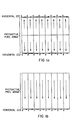
- High frame rate image sensors within the prior art have typically taught a photoactive pixel array split into rectangular sub-arrays of pixels, such as the high frame-rate, prior art sensor illustrated in Figures 1a and 1b.
- the signal from each of the sub-arrays in each of Figures 1a and 1b is read out serially through some output structure.
- the frame rate of the image sensor is governed by the number of sub-arrays combined with the speed of the serial output structure.
- the principle disadvantage of the type of arrangement shown in Figures 1a and 1b is that very high frame rates will require a large number of outputs for the pixel array.
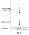
- Another type of high frame rate, image sensor utilizes the type of frame transfer image sensor shown in Figure 2.
- This type of sensor rapidly shifts the entire photoactive pixel array into a frame storage array. If the frame storage is made to hold more than one image, then a short sequence of images may be recorded at a high frame rate.
- the disadvantage of this type of sensor is that the frame rate is limited by how long it takes to shift the entire photoactive array into the storage array. Examples of this type of image sensor are given in U.S. Patent Nos.: 4,635,122, Kato et al, and 4,837,630, Ueda.
- An image sensor for recording images at a high frame rate is described using a frame, interline transfer type a sensor.
- the photoactive array of pixels is divided into two sections.
- the frame rate is governed by the time required to transfer an image into the storage array.
- the frame rate may be increased by subdividing the photoactive region into smaller segments. By utilizing a smaller segment of the photoactive pixel array the transfer time to the storage region is decreased and frame rate is increased. The number of frames that can be stored in the storage pixel array is also increased.
- a high frame rate image sensing device comprising: an array of pixels arranged in rows and columns such that the array is arranged into at least two equal sub-arrays, each pixel being capable of generating photoelectrons; a multiple phase vertical shift register allocated for each of the columns in the sub-arrays such that each of the pixels is associated with one of the shift registers; a transfer phase within the vertical shift registers that transfers photogenerated charges from the pixels into the vertical shift register; a plurality of transfer phase signals operatively connected to the transfer phases in the sub-arrays to created a plurality of zones; means for selecting a set of transfer phase signals for each of the zones to create a frame of selected pixels within the sub-array; a storage array for each of the sub-arrays operatively connected via the vertical shift registers to receive photogenerated charge from the pixels within the frames; and a horizontal shift register operatively connected to each of the storage arrays.
- the present invention overcomes the shortcomings of the prior art devices, such as those shown in Figures 1a, 1b and 2.
- the image sensor as envisioned by the present invention, and shown in Figure 3 consists of a photoactive pixel array 10 arranged in rows and columns, with two light shielded storage pixel arrays 14, 15.
- the preferred embodiment envisions that photoactive pixel array 10 be split into two pixel array halves 11, 12. Additionally, the pixel array 10 is divided into four zones A, B, C, and D with each of the top half of the pixel array 11 and the bottom half of the pixel array 12 having one half of each of the zones A, B, C, and D.
- the top pixel array half 11 employs top half vertical shift registers (VCCDs 24) to shift charge into the top storage pixel array 14.
- VCCDs 24 top half vertical shift registers
- bottom half of pixel array 12 will use bottom half vertical shift registers (VCCDs 25) to shift charge into the bottom storage pixel array 15.
- VCCDs 25 bottom half vertical shift registers
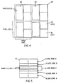
- FIG. 4 illustrates a block of four of pixels 20 within the photoactive pixel array 10.
- Each pixel 20 as seen in Fig. 4 is presumed to be in the same zone, accordingly, the control signals for each of the four pixels 20 will be the same. However, it should be understood that for pixels indifferent zones A, B, C and D the control signals (here the vertical shift register pulses) would be different.
- each of the four pixels 20 has a photodiode 22 adjacent to a cell in one of the vertical shift registers (VCCD 24, 25).
- the cell for the vertical shift register has two phases ⁇ 1, ⁇ 2.
- ⁇ 2 of the vertical CCD shift register (VCCD) for zones that are used in forming a frame is pulsed to transfer photoelectrons from the photodiodes 22 into the VCCDs 24, 25.
- the VCCDs 24, 25 rapidly shift the photoelectrons from every column of the photoactive pixels array into the storage pixel arrays 14, 15.
- the storage pixel storage arrays 14, 15 can store multiple frames. By selecting certain zones A, B, C, and D, the size of the top and bottom pixel arrays 11, 12 that are stored within the pixel storage arrays 14, 15 can be optimized for individual systems and uses. If each of the top and bottom pixel arrays 11, 12 having n/2 rows have all zones selected such that n/2 equals k , then the storage capacity is one top frame and one bottom frame.
- FIG. 5 shows a photoactive pixel array similar to that shown in Figure 3.
- the top and bottom halves of the photoactive pixel array are sectioned into three zones.
- Zone A contains Ra rows
- zone B contains Rb rows
- zone C contains Rc rows
- the photodiode readout pulse may be selectively applied to the ⁇ 2 phase of the vertical CCD shift register (VCCD) for zones that are used in forming a frame is pulsed to transfer photoelectrons from the photodiodes 22 into the VCCDs 24, 25. Therefore, each zone requires separate ⁇ 2 clocks indicated in Fig. 5 as V2A, V2B, V2C, and V2D.
- the photoelectrons are shifted through each zone of the VCCDs 24, 25 and into the storage pixel arrays 14, 15 by applying timing signals to the V1, V2A, V2B, V2C, V2D, V1S, and V2S input lines.
- V1S and V2S are used to clock pixel data through storage pixel arrays 14, 15. Accordingly, V1S and V2S are not active during a third level clocking on the ⁇ 2 clocks during which charge is transferred from the photodiodes to the vertical shift registers, this is to prevent pixel data gaps from occurring within the vertical shift registers.
- Zone A has now become part of the frame storage pixel array. Now it will require Rb + Rc + Rd VCCD clock cycles to transfer the image into the storage pixel array.
- the frame rate will be f/ ( fT + Rb + Rc + Rd ).
- zones C and D If the photodiode readout pulse is only applied to zones C and D, then only zones C and D will transfer photoelectrons from the photodiodes to the VCCD.
- the VCCD in zones A and B will not receive photoelectrons from the photodiodes.
- Zones A and B have now become part of the frame storage pixel array. Now it will require (Rc+Rd) VCCD clock cycles to transfer the image into the storage pixel array.
- the frame rate will be f/ ( fT + Rc + Rd ).
- zone D If the photodiode readout pulse is only applied to zone D, then only zone D will transfer photoelectrons from the photodiodes to the VCCD.
- the VCCD in zones A, B, and C will not receive photoelectrons from the photodiodes. Zones A, B, and C have now become part of the frame storage pixel array. Now it will require Rd VCCD clock cycles to transfer the image into the storage pixel array.
- the frame rate will be f/ ( fT + Rd ).
- the number of rows in the photoactive area and frame rate may be varied. Each one of the various frame rates would be available on one image sensor. The number of frames stored in the frame store would increase with smaller zones. For example, consider an embodiment where the photodiode readout time is 1.8 ⁇ s, the VCCD clock frequency is 5Mhz and the number of rows in each zone is listed in Table 1 below: Number of Rows Zone A 96 Zone B 48 Zone C 24 Zone D 24 Frame Store 29952
- this image sensor allows the number of rows in the image to be decreased in order to obtain very high frame rates.
- the advantage over the prior art is the ability to select the resolution and frame rate to best match the requirements of the imaging application.
Landscapes
- Engineering & Computer Science (AREA)
- Multimedia (AREA)
- Signal Processing (AREA)
- Solid State Image Pick-Up Elements (AREA)
- Transforming Light Signals Into Electric Signals (AREA)
Abstract
Description
| Number of Rows | |
| Zone A | 96 |
| Zone B | 48 |
| | 24 |
| | 24 |
| Frame Store | 29952 |
| Number of Columns | Total number of imaging rows | Frame Rate (frames/sec) | Frame store capacity |
| 512 | 384 | 25,000 | 78 |
| 512 | 192 | 47,000 | 157 |
| 512 | 96 | 87,000 | 315 |
| 512 | 48 | 151,000 | 631 |
Claims (10)
- A high frame rate image sensing device comprising:an array of pixels arranged in rows and columns such that the array is arranged into at least two equal sub-arrays, each pixel being capable of generating photoelectrons;a multiple phase vertical shift register allocated for each of the columns in the sub-arrays such that each of the pixels is associated with one of the shift registers;a transfer phase within the vertical shift registers that transfers photogenerated charges from the pixels into the vertical shift register;a plurality of transfer phase signals operatively connected to the transfer phases in the sub-arrays to created a plurality of zones;means for selecting a set of transfer phase signals for each of the zones to create a frame of selected pixels within the sub-array;a storage array for each of the sub-arrays operatively connected via the vertical shift registers to receive photogenerated charge from the pixels within the frames; anda horizontal shift register operatively connected to each of the storage arrays.
- The image sensing device of claim 1 wherein each of the sub-arrays have the same set of zones.
- The image sensing device of claim 1 wherein the vertical shift registers within the storage arrays have phases that are independent from the vertical shift registers in the sub-arrays.
- The image sensing device of claim 1 wherein the storage areas can hold an integral number of frames.
- The image sensor of claim 1 wherein the frame rate can be increased by selecting less than all the zones.
- A method for forming a high frame rate image sensing device comprising the steps of:providing an array of pixels arranged in rows and columns such that the array is arranged into at least two equal sub-arrays, each pixel being capable of generating photoelectrons with a multiple phase vertical shift register allocated for each of the columns in the sub-arrays such that each of the pixels is associated with one of the shift registers;forming a transfer phase within the vertical shift registers that transfers photogenerated charges from the pixels into the vertical shift register;connecting a plurality of transfer phase signals operatively connected to the transfer phases in the sub-arrays to created a plurality of zones;selecting a set of transfer phase signals for each of the zones to create a frame of selected pixels within the sub-array;operatively connecting a storage array for each of the sub-arrays via the vertical shift registers to receive photogenerated charge from the pixels within the frames; andoperatively connecting a horizontal shift register to each of the storage arrays.
- The method of claim 6 wherein the providing step further comprises providing each of the sub-arrays have the same set of zones.
- The method of claim 6 wherein the vertical shift registers within the storage arrays have phases that are independent from the vertical shift registers in the sub-arrays.
- The method of claim 1 wherein the frame rate can be increased by selecting less than all the zones.
- The image sensor of claim 9 wherein any unselected zones become part of the storage arrays.
Applications Claiming Priority (2)
| Application Number | Priority Date | Filing Date | Title |
|---|---|---|---|
| US36478599A | 1999-07-30 | 1999-07-30 | |
| US364785 | 1999-07-30 |
Publications (2)
| Publication Number | Publication Date |
|---|---|
| EP1073262A2 true EP1073262A2 (en) | 2001-01-31 |
| EP1073262A3 EP1073262A3 (en) | 2001-12-12 |
Family
ID=23436069
Family Applications (1)
| Application Number | Title | Priority Date | Filing Date |
|---|---|---|---|
| EP00202567A Withdrawn EP1073262A3 (en) | 1999-07-30 | 2000-07-17 | High speed image sensor |
Country Status (2)
| Country | Link |
|---|---|
| EP (1) | EP1073262A3 (en) |
| JP (1) | JP2001078094A (en) |
Cited By (2)
| Publication number | Priority date | Publication date | Assignee | Title |
|---|---|---|---|---|
| RU2673454C1 (en) * | 2018-01-23 | 2018-11-27 | Вячеслав Михайлович Смелков | Ring photo-receiver for panoramic television-computer scanning of monochrome image |
| CN113992870A (en) * | 2021-11-29 | 2022-01-28 | 中国电子科技集团公司第四十四研究所 | Large-array high-frame-frequency area array CCD |
Family Cites Families (6)
| Publication number | Priority date | Publication date | Assignee | Title |
|---|---|---|---|---|
| FR2548497B1 (en) * | 1983-06-28 | 1985-10-18 | Thomson Csf | IMAGE SENSOR WITH VARIABLE FORMAT FRAME TRANSFER |
| FR2594280B1 (en) * | 1986-02-07 | 1988-05-27 | Aerospatiale | OPTO-ELECTRONIC SENSOR WITH CHARGE TRANSFER |
| FR2604320B1 (en) * | 1986-09-19 | 1988-11-04 | Thomson Csf | FAST VIDEOGRAPHY SHOOTING SYSTEM USING A MATRIX OPTICAL SENSOR WITH LOAD TRANSFER |
| DE3877034T2 (en) * | 1987-04-10 | 1993-04-22 | Toshiba Kawasaki Kk | FIXED BODY IMAGE SCANNER WITH HIGH-SPEED SHUTTER AND METHOD FOR OBTAINING A HIGH SHUTTER SPEED IN A FIXED-BODY IMAGE SCANNER. |
| DE69020833T2 (en) * | 1989-09-14 | 1995-12-14 | Sony Corp | Charge-coupled imaging device with charge transfer parts horizontal in one imaging part. |
| JPH0767041A (en) * | 1993-08-30 | 1995-03-10 | Toshiba Corp | Driving method for solid-state imaging device |
-
2000
- 2000-07-17 EP EP00202567A patent/EP1073262A3/en not_active Withdrawn
- 2000-07-26 JP JP2000224756A patent/JP2001078094A/en active Pending
Cited By (2)
| Publication number | Priority date | Publication date | Assignee | Title |
|---|---|---|---|---|
| RU2673454C1 (en) * | 2018-01-23 | 2018-11-27 | Вячеслав Михайлович Смелков | Ring photo-receiver for panoramic television-computer scanning of monochrome image |
| CN113992870A (en) * | 2021-11-29 | 2022-01-28 | 中国电子科技集团公司第四十四研究所 | Large-array high-frame-frequency area array CCD |
Also Published As
| Publication number | Publication date |
|---|---|
| JP2001078094A (en) | 2001-03-23 |
| EP1073262A3 (en) | 2001-12-12 |
Similar Documents
| Publication | Publication Date | Title |
|---|---|---|
| EP1870937A1 (en) | Layout of control lines within an active pixel sensor | |
| EP0774870A2 (en) | Electronic image sensor | |
| US4803710A (en) | Storage registers with charge packet accumulation capability, as for solid-state imagers | |
| US4758895A (en) | Storage registers with charge packet accumulation capability, as for solid-state imagers | |
| US5491512A (en) | Solid state image sensor device and its driving method | |
| US4442457A (en) | Charge coupled device focal zoom | |
| KR920010511B1 (en) | Image pick-up device | |
| US5748232A (en) | Image sensor and driving method for the same | |
| EP0869664B1 (en) | Method for driving a solid state image sensor | |
| US4661854A (en) | Transfer smear reduction for charge sweep device imagers | |
| US20070139545A1 (en) | Image sensor for still or video photography | |
| US4862487A (en) | Solid-state imaging device | |
| US4577232A (en) | Line addressed charge coupled imager | |
| US8045025B2 (en) | Image pickup device adaptable to display fewer vertical pixels | |
| JPS63226177A (en) | Csd type solid-state image pickup element | |
| US7012644B1 (en) | Multiple output node charge coupled device | |
| JP3397151B2 (en) | Driving method of solid-state imaging device | |
| JPH0324873A (en) | Solid-state image pickup device | |
| JP2549106B2 (en) | Electronic shutter drive method for solid-state imaging device | |
| JP2001078094A (en) | Picture detector and its manufacture | |
| JPH0748828B2 (en) | Solid-state image sensor | |
| US5847757A (en) | Method of driving solid-state image sensing device | |
| JP3057898B2 (en) | Solid-state imaging device and driving method thereof | |
| JP3395257B2 (en) | Solid-state imaging device | |
| JPH10224697A (en) | Solid-state imaging device and method of driving solid-state imaging device |
Legal Events
| Date | Code | Title | Description |
|---|---|---|---|
| PUAI | Public reference made under article 153(3) epc to a published international application that has entered the european phase |
Free format text: ORIGINAL CODE: 0009012 |
|
| AK | Designated contracting states |
Kind code of ref document: A2 Designated state(s): DE FR GB NL Kind code of ref document: A2 Designated state(s): AT BE CH CY DE DK ES FI FR GB GR IE IT LI LU MC NL PT SE |
|
| AX | Request for extension of the european patent |
Free format text: AL;LT;LV;MK;RO;SI |
|
| PUAL | Search report despatched |
Free format text: ORIGINAL CODE: 0009013 |
|
| AK | Designated contracting states |
Kind code of ref document: A3 Designated state(s): AT BE CH CY DE DK ES FI FR GB GR IE IT LI LU MC NL PT SE |
|
| AX | Request for extension of the european patent |
Free format text: AL;LT;LV;MK;RO;SI |
|
| 17P | Request for examination filed |
Effective date: 20020514 |
|
| AKX | Designation fees paid |
Free format text: DE FR GB NL |
|
| 17Q | First examination report despatched |
Effective date: 20020724 |
|
| STAA | Information on the status of an ep patent application or granted ep patent |
Free format text: STATUS: THE APPLICATION IS DEEMED TO BE WITHDRAWN |
|
| 18D | Application deemed to be withdrawn |
Effective date: 20021204 |