EP1073168A1 - Modulator-integrated semiconductor laser and method of fabricating the same - Google Patents
Modulator-integrated semiconductor laser and method of fabricating the same Download PDFInfo
- Publication number
- EP1073168A1 EP1073168A1 EP00116432A EP00116432A EP1073168A1 EP 1073168 A1 EP1073168 A1 EP 1073168A1 EP 00116432 A EP00116432 A EP 00116432A EP 00116432 A EP00116432 A EP 00116432A EP 1073168 A1 EP1073168 A1 EP 1073168A1
- Authority
- EP
- European Patent Office
- Prior art keywords
- layer
- light waveguide
- embedding structure
- laser
- section
- Prior art date
- Legal status (The legal status is an assumption and is not a legal conclusion. Google has not performed a legal analysis and makes no representation as to the accuracy of the status listed.)
- Withdrawn
Links
- 239000004065 semiconductor Substances 0.000 title claims abstract description 31
- 238000004519 manufacturing process Methods 0.000 title claims description 6
- 239000000758 substrate Substances 0.000 claims abstract description 17
- 238000002310 reflectometry Methods 0.000 claims abstract description 14
- 238000000034 method Methods 0.000 claims description 19
- 229910000530 Gallium indium arsenide Inorganic materials 0.000 claims description 6
- 238000005253 cladding Methods 0.000 claims description 3
- 238000000059 patterning Methods 0.000 claims 1
- VYPSYNLAJGMNEJ-UHFFFAOYSA-N Silicium dioxide Chemical compound O=[Si]=O VYPSYNLAJGMNEJ-UHFFFAOYSA-N 0.000 description 10
- 230000000873 masking effect Effects 0.000 description 8
- 229920002120 photoresistant polymer Polymers 0.000 description 5
- 235000012239 silicon dioxide Nutrition 0.000 description 5
- 239000000377 silicon dioxide Substances 0.000 description 5
- 238000000206 photolithography Methods 0.000 description 4
- 239000013078 crystal Substances 0.000 description 3
- 238000005530 etching Methods 0.000 description 3
- 238000002347 injection Methods 0.000 description 3
- 239000007924 injection Substances 0.000 description 3
- 239000002184 metal Substances 0.000 description 3
- 230000000694 effects Effects 0.000 description 2
- 239000000463 material Substances 0.000 description 2
- 238000002230 thermal chemical vapour deposition Methods 0.000 description 2
- 238000001039 wet etching Methods 0.000 description 2
- 230000004888 barrier function Effects 0.000 description 1
- 230000008033 biological extinction Effects 0.000 description 1
- 230000005540 biological transmission Effects 0.000 description 1
- 238000005229 chemical vapour deposition Methods 0.000 description 1
- 238000000151 deposition Methods 0.000 description 1
- 238000010894 electron beam technology Methods 0.000 description 1
- 230000003287 optical effect Effects 0.000 description 1
- 230000003071 parasitic effect Effects 0.000 description 1
- 230000000149 penetrating effect Effects 0.000 description 1
- 238000000926 separation method Methods 0.000 description 1
- 239000000243 solution Substances 0.000 description 1
- 238000004544 sputter deposition Methods 0.000 description 1
- 238000000927 vapour-phase epitaxy Methods 0.000 description 1
Images





Classifications
-
- H—ELECTRICITY
- H01—ELECTRIC ELEMENTS
- H01S—DEVICES USING THE PROCESS OF LIGHT AMPLIFICATION BY STIMULATED EMISSION OF RADIATION [LASER] TO AMPLIFY OR GENERATE LIGHT; DEVICES USING STIMULATED EMISSION OF ELECTROMAGNETIC RADIATION IN WAVE RANGES OTHER THAN OPTICAL
- H01S5/00—Semiconductor lasers
- H01S5/02—Structural details or components not essential to laser action
- H01S5/026—Monolithically integrated components, e.g. waveguides, monitoring photo-detectors, drivers
- H01S5/0265—Intensity modulators
-
- H—ELECTRICITY
- H01—ELECTRIC ELEMENTS
- H01S—DEVICES USING THE PROCESS OF LIGHT AMPLIFICATION BY STIMULATED EMISSION OF RADIATION [LASER] TO AMPLIFY OR GENERATE LIGHT; DEVICES USING STIMULATED EMISSION OF ELECTROMAGNETIC RADIATION IN WAVE RANGES OTHER THAN OPTICAL
- H01S5/00—Semiconductor lasers
- H01S5/20—Structure or shape of the semiconductor body to guide the optical wave ; Confining structures perpendicular to the optical axis, e.g. index or gain guiding, stripe geometry, broad area lasers, gain tailoring, transverse or lateral reflectors, special cladding structures, MQW barrier reflection layers
- H01S5/22—Structure or shape of the semiconductor body to guide the optical wave ; Confining structures perpendicular to the optical axis, e.g. index or gain guiding, stripe geometry, broad area lasers, gain tailoring, transverse or lateral reflectors, special cladding structures, MQW barrier reflection layers having a ridge or stripe structure
- H01S5/227—Buried mesa structure ; Striped active layer
-
- H—ELECTRICITY
- H01—ELECTRIC ELEMENTS
- H01S—DEVICES USING THE PROCESS OF LIGHT AMPLIFICATION BY STIMULATED EMISSION OF RADIATION [LASER] TO AMPLIFY OR GENERATE LIGHT; DEVICES USING STIMULATED EMISSION OF ELECTROMAGNETIC RADIATION IN WAVE RANGES OTHER THAN OPTICAL
- H01S5/00—Semiconductor lasers
- H01S5/04—Processes or apparatus for excitation, e.g. pumping, e.g. by electron beams
- H01S5/042—Electrical excitation ; Circuits therefor
- H01S5/0425—Electrodes, e.g. characterised by the structure
- H01S5/04256—Electrodes, e.g. characterised by the structure characterised by the configuration
-
- H—ELECTRICITY
- H01—ELECTRIC ELEMENTS
- H01S—DEVICES USING THE PROCESS OF LIGHT AMPLIFICATION BY STIMULATED EMISSION OF RADIATION [LASER] TO AMPLIFY OR GENERATE LIGHT; DEVICES USING STIMULATED EMISSION OF ELECTROMAGNETIC RADIATION IN WAVE RANGES OTHER THAN OPTICAL
- H01S5/00—Semiconductor lasers
- H01S5/20—Structure or shape of the semiconductor body to guide the optical wave ; Confining structures perpendicular to the optical axis, e.g. index or gain guiding, stripe geometry, broad area lasers, gain tailoring, transverse or lateral reflectors, special cladding structures, MQW barrier reflection layers
- H01S5/2054—Methods of obtaining the confinement
- H01S5/2059—Methods of obtaining the confinement by means of particular conductivity zones, e.g. obtained by particle bombardment or diffusion
- H01S5/2063—Methods of obtaining the confinement by means of particular conductivity zones, e.g. obtained by particle bombardment or diffusion obtained by particle bombardment
-
- H—ELECTRICITY
- H01—ELECTRIC ELEMENTS
- H01S—DEVICES USING THE PROCESS OF LIGHT AMPLIFICATION BY STIMULATED EMISSION OF RADIATION [LASER] TO AMPLIFY OR GENERATE LIGHT; DEVICES USING STIMULATED EMISSION OF ELECTROMAGNETIC RADIATION IN WAVE RANGES OTHER THAN OPTICAL
- H01S5/00—Semiconductor lasers
- H01S5/20—Structure or shape of the semiconductor body to guide the optical wave ; Confining structures perpendicular to the optical axis, e.g. index or gain guiding, stripe geometry, broad area lasers, gain tailoring, transverse or lateral reflectors, special cladding structures, MQW barrier reflection layers
- H01S5/2054—Methods of obtaining the confinement
- H01S5/2077—Methods of obtaining the confinement using lateral bandgap control during growth, e.g. selective growth, mask induced
Definitions
- the present Invention relates generally to semiconductor lasers and more specifically to a modulator-integrated semiconductor laser.
- semiconductor lasers are essential elements and their ability to modulate the laser beam with information signals is an important factor to achieve high speed transmission.
- One approach to achieving this goal is to reduce the device capacitance.
- a light waveguide including the active layer of the laser is buried in an InP embedding layer and a contact layer such as InGaAs or InGaAsP is formed on the embedding layer.
- the embedding layer are selectively implanted with protons to create high resistance regions on the opposite side portions of the active layer.
- injection current is efficiently utilized by the active layer.
- An electrode is then formed on the contact layer.
- the contact layer is formed of the material known to exhibit inability to become highly resistive when subjected to a beam of protons
- the electrode that extends over the full area of the device contributes to an increase in the device capacitance, which prevents the laser from operating at a speed of 10 Gb/s or higher.
- Another approach to reducing device capacitance is to employ a pad electrode structure.
- the InP embedding layer is less of the ability to become highly resistive than is the InGaAs or InGaAsP contact layer.
- parasitic capacitances may exist between the proton implanted high resistance regions and the electrode.
- a semiconductor laser comprising a semiconductor substrate having a laser section and a modulator section, and a light waveguide having an active layer on the substrate and extending across the laser section and the modulator section from a high reflectivity end portion to a low reflectivity end portion.
- An embedding structure encloses the light waveguide.
- the embedding structure has a pair of high resistance regions one on each side of the light waveguide for confining electrons between the high resistance regions.
- First and second elongated contact regions are formed on the embedding structure corresponding respectively to the laser section and the modulator section.
- An insulating layer is provided for covering portions other than the first and second elongated contact regions.
- First and second electrodes are formed on the insulating layer for establishing ohmic contact with the first and second elongated contact regions, respectively.
- the present Invention provides a method of fabricating a semiconductor laser comprising the steps of (a) forming a light waveguide having an active layer on a semiconductor substrate having a laser section and a modulator section, the light waveguide extending across the laser section and the modulator section from a high reflectivity end portion to a low reflectivity end portion, (b) forming an embedding structure for enclosing the light waveguide, (c) forming first and second elongated contact regions on the embedding structure corresponding respectively to the laser section and the modulator section and producing first and second high resistance regions in the embedding structure on opposite sides of the light waveguide so that electrons are confined between the first and second high resistance regions, (d) forming an insulating layer for covering portions of the semiconductor laser other than the first and second elongated contact regions, and (e) forming first and second electrodes on the insulating layer for establishing ohmic contact with the first and second elongated contact regions, respectively.
- a modulator-integrated DFB (distributed feedback) semiconductor laser of a first embodiment of this invention are illustrated.
- a quaternary semiconductor such as InGaAsP is used as an active layer of the modulator-integrated semiconductor laser.
- an array of such laser devices are defined on a semiconductor wafer. For purposes of the disclosure, only one laser device is illustrated.
- an n-type InP semiconductor substrate 101 is illustrated having a crystal plane (100) as a principle surface of the substrate.
- the n-InP substrate has a laser section 102 and a modulator section 104.
- the crystal plane (100) is irradiated with an electron beam in the direction ⁇ 011 ⁇ of the substrate to form within a 400 ⁇ m x 10 ⁇ m rectangular area a resist pattern at intervals of 241.7 nm in the laser section 102.
- a diffraction grating 103 is then formed in the rectangular area by subjecting the device to an appropriate etching solution.
- a pair of masking films 105 of silicon dioxide is formed across the whole length of the device so that the side portions of diffraction grating 103 and the extensions of such side portions are shielded from penetrating active molecules used in subsequent selective-area epitaxial growth processes.
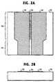
- the surface of each masking film 105 is tapered so that its width in the modulator section 104 is narrower than it is in the laser section 102, as shown in Figs. 2A and 2B. More specifically, the masking films are formed by using the thermal CVD (chemical vapor deposition) method for depositing a 100-nm thick silicon dioxide layer.
- Photolithography and wet etching processes are then used to pattern the silicon dioxide film into a pair of stripes with a spacing of 1.5 ⁇ m therebetween in the crystal direction ⁇ 011 ⁇ , and with a width of 18 ⁇ m and a length of 400 ⁇ m in the laser section 102 and a width of 5 ⁇ m and a length of 200 ⁇ m in the modulator section 104.
- a selective-area epitaxial process such as metal organic vapor phase epitaxy (MOVPE) is performed by subjecting the device in a reactive environment maintained at a pressure of 75 Torr and an elevated temperature of 625°C to form a 0.1- ⁇ m thick InGaAsP guide layer 61 with a carrier concentration of 5 x 10 17 cm -3 and a bandgap of 1.13 ⁇ m.
- An active layer 62 is then deposited.
- This active layer is a multiple-quantum-well (MQW) system consisting of 6-nm thick InGaAsP well layers with a bandgap of 1.56 ⁇ m in the laser section 102 and 1.47 ⁇ m in the modulator section 104.
- MQW multiple-quantum-well
- These well layers are alternately sandwiched between 8-nm thick barrier layers with a bandgap of 1.13 ⁇ m in the laser section 102 and 1.47 ⁇ m in the modulator section 104.
- On the active layer 62 is epitaxially grown a 60-nm thick InGaAsP light confinement layer 63 with a carrier concentration of 5 x 10 17 cm -3 and a bandgap of 1.13 ⁇ m.
- On the light confinement layer 63 is a 0.1- ⁇ m thick p-type InP cladding layer 64 having a carrier concentration of 5 x 10 17 cm -3 and a bandgap of 1.13 ⁇ m.
- the epitaxial layers 61 to 64 are formed on the areas not covered with the masking films 105.
- the epitaxial layers 61 to 64 formed in the central region of the device constitute a light waveguide 106 that extends at constant width along the length of the device.
- the inner edges of the masking films 105 are then etched so that they are separated a dietance of 8 ⁇ m apart from each other, revealing portions of the principle surface of substrate 101 on the opposite sides of the light waveguide 106.
- a selective-area MOVPE process is then performed by subjecting the device in a reactive environment maintained at a pressure of 75 Torr and an elevated temperature of 625°C to epitaxially grow a mesa type laminated embedding structure 107 consisting of a 0.3 ⁇ m thick p-type InP layer with a carrier concentration of 5 x 10 17 cm -3 and a 1.5 ⁇ m thick p-type InP layer with a carrier concentration of 1 x 10 18 cm -3 .
- the light waveguide 106 is buried in the embedding structure 107.
- the upper surface of the mesa type structure 107 is covered with a 0.2 ⁇ m thick epitaxial InGaAs contact layer 108 with a carrier concentration of 5 x 10 18 cm -3 .
- Contact layer 108 has a constant width of preferably 5 ⁇ m or less along the length of the device.
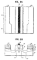
- a photoresist stripe 109 is formed on the contact layer 108 using photolithography, as shown in Figs. 5A and 5B.
- the width of this photoresist stripe is 2 ⁇ 3 ⁇ m which is wider than the width of light waveguide 106 embedded below the contact layer 108.
- the device is then subjected to a beam of protons accelerated at 200 kilovolts so that the device is injected with protons as indicated by a dotted line 130 to a dose of 1 x 10 15 cm -2 .
- a high resistance region 110 is produced in the embedding structure 107 on each side of the light waveguide 106. These high resistance regions have the effect of confining electrons in a narrow region surrounding the light waveguide 106.
- Photoresist mask 109 is removed as shown in Figs. 6A, 6B to reveal the contact layer 108.
- the revealed contact layer 108 is then divided by a region 116 (with a separation of 25 to 50 ⁇ m) into two contact regions 108A and 108B respectively corresponding to the laser section 102 and the modulator section 104.
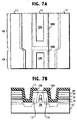
- a silicon dioxide layer 111 is then deposited over the device to a thickness of 350 nm, as shown in Figs. 7A and 7B, by using the thermal CVD method, and then etched to form a rectangular contact window 120 on each of the laser end modulator sections 102 and 104 to reveal portions of the underlying contact layer 108, using photolithography and wet etching.
- a metal layer of Ti/Au is deposited on each of the contact regions through each of the contact windows 120A, 120B to a thickness of 100 to 300 nm using a sputtering method and then patterned into positive electrodes 112A, 112B of pad structure, as shown in Figs. 8A, 8B.
- the bottom surface of the substrate 101 is formed is lapped and a negative Ti/Au electrode 113 is deposited on the bottom of each substrate.
- the negative electrode 113 has the same thickness as the positive electrode 112.
- the wafer is then cleaved to separate the individual devices.
- a reflecting film 114 of 90 % reflectivity is attached to one end of the device near the laser section 102 and are reflective film 115 of 0.1% reflectivity is attached to the opposite end.
- the width of contact regions 108A, 108B that extend over the light waveguide 109 is as small as 5 ⁇ m as described above and since these contact regions are not alterable to high resistive material when the device is subjected to proton injection, the capacitance of the device as measured between the high resistance regions 110 and the positive electrodes 112A, 112B can be significantly reduced in comparison with the prior art device.
- Tests conducted on the laser manufactured according to the present invention indicate that the capacitance of the integrated modulator is 0.4 pF at a bias voltage of -1 volt and the cut-off frequency of the modulator for low level modulating signals is 15 GHz.
- the laser was operated at a modulation rate of 10 Gb/s, the eye pattern of sufficiently clear opening was obtained.
- the extinction ratio of the device when the modulator is operated on a reverse bias voltage of 2 volts is more than 15 dB which is comparable to the value attainable with conventional lasers.
- an injection current of 100 mA the laser delivered a 15 mW output.
- Figs. 9A, 9B to 11A, 11B show an alternative embodiment of the present inverttion which is similar to Figs. 1A, 1B to 3A, 3B.
- the masking films 105 are completely removed as opposed to the previous embodiment in which only side portions of the light waveguide 109 are removed.
- a selective-area MOVPE process is provided by subjecting the device in a reactive environment maintained at a pressure of 75 Torr and an elevated temperature of 625°C to epitaxially grow a laminated embedding structure 207 consisting of p-type InP layer with a carrier concentration of 5 x 10 17 cm -3 and a p-type InP layer with a carrier concentration of 1 x 10 18 cm -3 . Due to the absence of masking films, the embedding structure 207 covers the whole area of the device. The embedding structure 207 is then polished until it presents a flat upper surface. The upper surface of the embedding structure 207 is fully covered with a 0.2 ⁇ m thick epitaxial InGaAs contact layer 208 with a carrier concentration of 5 x 10 18 cm -3 .
- a striped photoresist mask 209 with a width of 2 to 3 ⁇ m is formed on the contact layer 208 in a position immediately above the light waveguide 106, as shown in Figs. 10A, 10B.
- the device is then subjected to a beam of protons accelerated at 200 kilovolts with a dose of 1 x 10 15 cm -2 to produce a high resistance region 210 on each side of the light waveguide 106.
- Photoresist mask 209 is then removed, followed by an etching process in which portions of the conductive layer 208 are removed such that it leaves a center portion of the layer 208 that lies above the light waveguide 106. Note that the width of this center portion of the layer 208 is about 5 ⁇ m which equals the width of contact layer 108 of the previous embodiment. With this etching process, the contact layer 208 is separated into two contact regions corresponding to the laser section 102 and the modulator section 104.
- a silicon dioxide layer 211 is then deposited over the device to a thickness of 350 nm, as shown in Figs. 11A, 11B and then etched to form a rectangular contact window on each of the laser and modulator sections 102 and 104 to reveal portions of the underlying contact layer 208.
- a metal layer of Ti/Au is deposited on each of the contact regions through each contact window to a thickness of 100 to 300 nm and then patterned into positive electrodes 212A, 212B of pad structure.
- the bottom surface of the wafer is lapped and a negative electrode 213 is deposited on the bottom of the substrate and the wafer Is then cleaved to separate the individual devices.
- a reflecting film 214 of 90 % reflectivity is attached to one end of the device near the laser section 102 and a reflective film 215 of 0.1 % reflectivity is attached to the opposite end.
Landscapes
- Physics & Mathematics (AREA)
- Condensed Matter Physics & Semiconductors (AREA)
- General Physics & Mathematics (AREA)
- Electromagnetism (AREA)
- Optics & Photonics (AREA)
- Geometry (AREA)
- Semiconductor Lasers (AREA)
- Optical Modulation, Optical Deflection, Nonlinear Optics, Optical Demodulation, Optical Logic Elements (AREA)
Abstract
Description
- The present Invention relates generally to semiconductor lasers and more specifically to a modulator-integrated semiconductor laser.
- For optical communications systems, semiconductor lasers are essential elements and their ability to modulate the laser beam with information signals is an important factor to achieve high speed transmission. One approach to achieving this goal is to reduce the device capacitance. In conventional semiconductor lasers, a light waveguide including the active layer of the laser is buried in an InP embedding layer and a contact layer such as InGaAs or InGaAsP is formed on the embedding layer. Through the contact layer, the embedding layer are selectively implanted with protons to create high resistance regions on the opposite side portions of the active layer. As a result of the carrier confinement effect of the high resistance regions, injection current is efficiently utilized by the active layer. An electrode is then formed on the contact layer. Although the contact layer is formed of the material known to exhibit inability to become highly resistive when subjected to a beam of protons, the electrode that extends over the full area of the device contributes to an increase in the device capacitance, which prevents the laser from operating at a speed of 10 Gb/s or higher.
- Another approach to reducing device capacitance is to employ a pad electrode structure. However, the InP embedding layer is less of the ability to become highly resistive than is the InGaAs or InGaAsP contact layer. Thus, parasitic capacitances may exist between the proton implanted high resistance regions and the electrode.
- It is therefore an object of the present invention to provide a semiconductor laser having a reduced capacitance, and a method of fabricating the laser for high speed operation.
- According to a first aspect of the present invention, there is provided a semiconductor laser comprising a semiconductor substrate having a laser section and a modulator section, and a light waveguide having an active layer on the substrate and extending across the laser section and the modulator section from a high reflectivity end portion to a low reflectivity end portion. An embedding structure encloses the light waveguide. The embedding structure has a pair of high resistance regions one on each side of the light waveguide for confining electrons between the high resistance regions. First and second elongated contact regions are formed on the embedding structure corresponding respectively to the laser section and the modulator section. An insulating layer is provided for covering portions other than the first and second elongated contact regions. First and second electrodes are formed on the insulating layer for establishing ohmic contact with the first and second elongated contact regions, respectively.
- According to a second aspect, the present Invention provides a method of fabricating a semiconductor laser comprising the steps of (a) forming a light waveguide having an active layer on a semiconductor substrate having a laser section and a modulator section, the light waveguide extending across the laser section and the modulator section from a high reflectivity end portion to a low reflectivity end portion, (b) forming an embedding structure for enclosing the light waveguide, (c) forming first and second elongated contact regions on the embedding structure corresponding respectively to the laser section and the modulator section and producing first and second high resistance regions in the embedding structure on opposite sides of the light waveguide so that electrons are confined between the first and second high resistance regions, (d) forming an insulating layer for covering portions of the semiconductor laser other than the first and second elongated contact regions, and (e) forming first and second electrodes on the insulating layer for establishing ohmic contact with the first and second elongated contact regions, respectively.
- The present invention will be described in further detail with reference to the accompanying drawings, in which;
- Figs. 1A to 8A are top plan views of a modulator-integrated semiconductor laser of successive stages of a fabrication process according to a first embodiment of the present invention;
- Figs. 1B to 8B are end views of the modulator-integrated semiconductor laser corresponding to Figs. 1A to 8A, respectively;
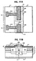
- Figs. 9A to 11A are top plan views of a modulator-integrated semiconductor laser of successive stages of a fabrication process according to a second embodiment of the present invention; and
- Figs. 9B to 11B are end views of the modulator-integrated semiconductor laser corresponding to Figs. 9A to 11A, respectively.
-
- Referring now to Figs. 1A, 1B to 8A, 8B, successive stages of a process of fabricating a modulator-integrated DFB (distributed feedback) semiconductor laser of a first embodiment of this invention are illustrated. In the present invention, a quaternary semiconductor such as InGaAsP is used as an active layer of the modulator-integrated semiconductor laser. In a practical aspect, an array of such laser devices are defined on a semiconductor wafer. For purposes of the disclosure, only one laser device is illustrated.
- As shown in Figs. 1A and 1B, an n-type
InP semiconductor substrate 101 is illustrated having a crystal plane (100) as a principle surface of the substrate. The n-InP substrate has alaser section 102 and amodulator section 104. First, the crystal plane (100) is irradiated with an electron beam in the direction 〈011〉 of the substrate to form within a 400 µm x 10 µm rectangular area a resist pattern at intervals of 241.7 nm in thelaser section 102. A diffraction grating 103 is then formed in the rectangular area by subjecting the device to an appropriate etching solution. - A pair of
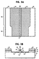
masking films 105 of silicon dioxide is formed across the whole length of the device so that the side portions of diffraction grating 103 and the extensions of such side portions are shielded from penetrating active molecules used in subsequent selective-area epitaxial growth processes. At the interface between thelaser section 102 and themodulator section 104, the surface of eachmasking film 105 is tapered so that its width in themodulator section 104 is narrower than it is in thelaser section 102, as shown in Figs. 2A and 2B. More specifically, the masking films are formed by using the thermal CVD (chemical vapor deposition) method for depositing a 100-nm thick silicon dioxide layer. Photolithography and wet etching processes are then used to pattern the silicon dioxide film into a pair of stripes with a spacing of 1.5 µm therebetween in the crystal direction 〈011〉, and with a width of 18 µm and a length of 400 µm in thelaser section 102 and a width of 5 µm and a length of 200 µm in themodulator section 104. - As shown in Figs. 3A and 3B, a selective-area epitaxial process such as metal organic vapor phase epitaxy (MOVPE) is performed by subjecting the device in a reactive environment maintained at a pressure of 75 Torr and an elevated temperature of 625°C to form a 0.1-µm thick
InGaAsP guide layer 61 with a carrier concentration of 5 x 1017 cm-3 and a bandgap of 1.13 µm. Anactive layer 62 is then deposited. This active layer is a multiple-quantum-well (MQW) system consisting of 6-nm thick InGaAsP well layers with a bandgap of 1.56 µm in thelaser section 102 and 1.47 µm in themodulator section 104. These well layers are alternately sandwiched between 8-nm thick barrier layers with a bandgap of 1.13 µm in thelaser section 102 and 1.47 µm in themodulator section 104. On theactive layer 62 is epitaxially grown a 60-nm thick InGaAsPlight confinement layer 63 with a carrier concentration of 5 x 1017 cm-3 and a bandgap of 1.13 µm. On thelight confinement layer 63 is a 0.1-µm thick p-typeInP cladding layer 64 having a carrier concentration of 5 x 1017 cm-3 and a bandgap of 1.13 µm. Thus, theepitaxial layers 61 to 64 are formed on the areas not covered with themasking films 105. Theepitaxial layers 61 to 64 formed in the central region of the device constitute alight waveguide 106 that extends at constant width along the length of the device. - The inner edges of the
masking films 105 are then etched so that they are separated a dietance of 8 µm apart from each other, revealing portions of the principle surface ofsubstrate 101 on the opposite sides of thelight waveguide 106. - As shown in Figs. 4A and 4B, a selective-area MOVPE process is then performed by subjecting the device in a reactive environment maintained at a pressure of 75 Torr and an elevated temperature of 625°C to epitaxially grow a mesa type laminated
embedding structure 107 consisting of a 0.3 µm thick p-type InP layer with a carrier concentration of 5 x 1017 cm-3 and a 1.5 µm thick p-type InP layer with a carrier concentration of 1 x 1018 cm-3. As a result, thelight waveguide 106 is buried in theembedding structure 107. The upper surface of themesa type structure 107 is covered with a 0.2 µm thick epitaxialInGaAs contact layer 108 with a carrier concentration of 5 x 1018 cm-3.Contact layer 108 has a constant width of preferably 5 µm or less along the length of the device. - A
photoresist stripe 109 is formed on thecontact layer 108 using photolithography, as shown in Figs. 5A and 5B. The width of this photoresist stripe is 2 ∼ 3 µm which is wider than the width oflight waveguide 106 embedded below thecontact layer 108. The device is then subjected to a beam of protons accelerated at 200 kilovolts so that the device is injected with protons as indicated by a dottedline 130 to a dose of 1 x 1015 cm-2. As a result, ahigh resistance region 110 is produced in the embeddingstructure 107 on each side of thelight waveguide 106. These high resistance regions have the effect of confining electrons in a narrow region surrounding thelight waveguide 106. -
Photoresist mask 109 is removed as shown in Figs. 6A, 6B to reveal thecontact layer 108. The revealedcontact layer 108 is then divided by a region 116 (with a separation of 25 to 50 µm) into twocontact regions laser section 102 and themodulator section 104. - A
silicon dioxide layer 111 is then deposited over the device to a thickness of 350 nm, as shown in Figs. 7A and 7B, by using the thermal CVD method, and then etched to form a rectangular contact window 120 on each of the laserend modulator sections underlying contact layer 108, using photolithography and wet etching. - A metal layer of Ti/Au is deposited on each of the contact regions through each of the
contact windows positive electrodes substrate 101 is formed is lapped and a negative Ti/Au electrode 113 is deposited on the bottom of each substrate. Thenegative electrode 113 has the same thickness as the positive electrode 112. The wafer is then cleaved to separate the individual devices. A reflectingfilm 114 of 90 % reflectivity is attached to one end of the device near thelaser section 102 and arereflective film 115 of 0.1% reflectivity is attached to the opposite end. - Since the width of
contact regions light waveguide 109 is as small as 5 µm as described above and since these contact regions are not alterable to high resistive material when the device is subjected to proton injection, the capacitance of the device as measured between thehigh resistance regions 110 and thepositive electrodes - Tests conducted on the laser manufactured according to the present invention indicate that the capacitance of the integrated modulator is 0.4 pF at a bias voltage of -1 volt and the cut-off frequency of the modulator for low level modulating signals is 15 GHz. When the laser was operated at a modulation rate of 10 Gb/s, the eye pattern of sufficiently clear opening was obtained. Further, the extinction ratio of the device when the modulator is operated on a reverse bias voltage of 2 volts is more than 15 dB which is comparable to the value attainable with conventional lasers. Further, with an injection current of 100 mA, the laser delivered a 15 mW output.
- Figs. 9A, 9B to 11A, 11B show an alternative embodiment of the present inverttion which is similar to Figs. 1A, 1B to 3A, 3B. With the laser device obtained as shown in Figs. 3A, 3B, the masking
films 105 are completely removed as opposed to the previous embodiment in which only side portions of thelight waveguide 109 are removed. - With the masking
films 105 being completely removed (Figs. 9A, 9B), a selective-area MOVPE process is provided by subjecting the device in a reactive environment maintained at a pressure of 75 Torr and an elevated temperature of 625°C to epitaxially grow a laminated embeddingstructure 207 consisting of p-type InP layer with a carrier concentration of 5 x 1017 cm-3 and a p-type InP layer with a carrier concentration of 1 x 1018 cm-3. Due to the absence of masking films, the embeddingstructure 207 covers the whole area of the device. The embeddingstructure 207 is then polished until it presents a flat upper surface. The upper surface of the embeddingstructure 207 is fully covered with a 0.2 µm thick epitaxialInGaAs contact layer 208 with a carrier concentration of 5 x 1018 cm-3. - Using photolithography, a
striped photoresist mask 209 with a width of 2 to 3 µm is formed on thecontact layer 208 in a position immediately above thelight waveguide 106, as shown in Figs. 10A, 10B. The device is then subjected to a beam of protons accelerated at 200 kilovolts with a dose of 1 x 1015 cm-2 to produce ahigh resistance region 210 on each side of thelight waveguide 106. -
Photoresist mask 209 is then removed, followed by an etching process in which portions of theconductive layer 208 are removed such that it leaves a center portion of thelayer 208 that lies above thelight waveguide 106. Note that the width of this center portion of thelayer 208 is about 5 µm which equals the width ofcontact layer 108 of the previous embodiment. With this etching process, thecontact layer 208 is separated into two contact regions corresponding to thelaser section 102 and themodulator section 104. - A
silicon dioxide layer 211 is then deposited over the device to a thickness of 350 nm, as shown in Figs. 11A, 11B and then etched to form a rectangular contact window on each of the laser andmodulator sections underlying contact layer 208. A metal layer of Ti/Au is deposited on each of the contact regions through each contact window to a thickness of 100 to 300 nm and then patterned intopositive electrodes 212A, 212B of pad structure. As in the previous embodiment, the bottom surface of the wafer is lapped and anegative electrode 213 is deposited on the bottom of the substrate and the wafer Is then cleaved to separate the individual devices. A reflectingfilm 214 of 90 % reflectivity is attached to one end of the device near thelaser section 102 and areflective film 215 of 0.1 % reflectivity is attached to the opposite end.
Claims (14)
- A semiconductor laser comprising:a semiconductor substrate having a laser section and a modulator section;a light waveguide having an active layer on said substrate and extending across said laser section and said modulator section from a high reflectivity end portion to a low reflectivity end portion;an embedding structure for enclosing said light waveguide, the embedding structure having a pair of high resistance regions one on each side of the light waveguide for confining electrons between said high resistance regions;first and second elongated contact regions formed on said embedding structure corresponding respectively to said laser section and said modulator section;an insulating layer far covering portions other than said first and second elongated contact regions; andfirst and second electrodes formed on said insulating layer for establishing ohmic contact with said first and second contact regions, respectively.
- The semiconductor laser of claim 1, wherein each of said first and second elongated contact regions and said embedding structure have a substantially same width.
- The semiconductor laser of claim 1, wherein said embedding structure is formed of InP and said high resistance regions are implanted with protons and said first and second elongated contact regions are formed of InGaAsP or InGaAs.
- The semiconductor laser of claim 1, wherein the laser section of said substrate is formed with a diffraction grating and wherein a portion of said light waveguide is formed on said diffraction grating.
- The semiconductor laser of claim 1, wherein said first and second contact regions have a width of 5 µm or less.
- The semiconductor laser of claim 1, wherein said light waveguide further comprises a guide layer on which said active layer is formed, a light confinement layer on the active layer and a cladding layer on the light confinement layer.
- A method of fabricating a semiconductor laser comprising the steps of:a) forming a light waveguide having an active layer on a semiconductor substrate having a laser section and a modulator section, the light waveguide extending across said laser section and said modulator section from a high reflectivity end portion to a low reflectivity end portion;b) forming an embedding structure for enclosing said light waveguide;c) forming first and second elongated contact regions on said embedding structure corresponding respectively to said laser section and said modulator section and producing first and second high resistance regions In said embedding structure on opposite sides of the light waveguide so that electrons are confined between said first and second high resistance regions;d) forming an insulating layer for covering portions of the semiconductor laser other than said first and second elongated contact regions; ande) forming first and second electrodes on said insulating layer for establishing ohmic contact with said first and second elongated contact regions, respectively.
- The method of claim 7, wherein the step (c) comprises the steps of:epitaxially growing an elongated contact layer on said embedding structure;forming an elongated resist mask on said elongated contact layer above said embedded light waveguide;implanting protons into said embedding structure so that said first and second high resistive portions are produced on opposite sides of said light waveguide;removing said elongated resist mask; andseparating said elongated contact layer into said first and second elongated contact regions.
- The method of claim 7, wherein the step (c) comprises the steps of:epitaxially growing a contact layer on said embedding structure;forming an elongated resist mask on said contact layer above said embedded light waveguide;implanting protons into said embedding structure so that said first and second high resistive portions are produced on opposite sides of said light waveguide;removing said elongated resist mask; andpatterning said contact layer into said first and second elongated contact regions.
- The method of claim 7, wherein each of said first and second elongated contact regions and said embedding structure have a substantially same width.
- The method of claim 7, wherein said embedding structure is formed of InP and said first and second elongated contact regions are formed of InGaAsP or InGaAs.
- The method of claim 7, wherein the step (a) comprises the step of forming a diffraction grating and forming said portion of said light waveguide on said diffraction grating.
- The method of claim 7, wherein said first and second contact regions have a width of 5 µm or less.
- The method of claim 7, wherein said light waveguide further comprises a guide layer on which said active layer is formed, a light confinement layer on the active layer and a cladding layer on the light confinement layer.
Applications Claiming Priority (2)
| Application Number | Priority Date | Filing Date | Title |
|---|---|---|---|
| JP21358099 | 1999-07-28 | ||
| JP21358099A JP2001044566A (en) | 1999-07-28 | 1999-07-28 | Semiconductor laser and manufacture thereof |
Publications (1)
| Publication Number | Publication Date |
|---|---|
| EP1073168A1 true EP1073168A1 (en) | 2001-01-31 |
Family
ID=16641563
Family Applications (1)
| Application Number | Title | Priority Date | Filing Date |
|---|---|---|---|
| EP00116432A Withdrawn EP1073168A1 (en) | 1999-07-28 | 2000-07-28 | Modulator-integrated semiconductor laser and method of fabricating the same |
Country Status (3)
| Country | Link |
|---|---|
| US (1) | US6489177B1 (en) |
| EP (1) | EP1073168A1 (en) |
| JP (1) | JP2001044566A (en) |
Cited By (1)
| Publication number | Priority date | Publication date | Assignee | Title |
|---|---|---|---|---|
| WO2003047055A1 (en) * | 2001-11-30 | 2003-06-05 | Optillion Ab | Laser modulator |
Families Citing this family (7)
| Publication number | Priority date | Publication date | Assignee | Title |
|---|---|---|---|---|
| US6694069B2 (en) * | 2000-10-30 | 2004-02-17 | Kyocera Corporation | Optical integrated circuit substrate and optical module |
| JP2002344067A (en) * | 2001-05-21 | 2002-11-29 | Sumitomo Electric Ind Ltd | Method for manufacturing optical integrated device |
| US7057214B2 (en) * | 2003-07-01 | 2006-06-06 | Optiswitch Technology Corporation | Light-activated semiconductor switches |
| JP2006269581A (en) * | 2005-03-23 | 2006-10-05 | Mitsubishi Electric Corp | Semiconductor laser device |
| US8451563B1 (en) * | 2011-12-20 | 2013-05-28 | Western Digital (Fremont), Llc | Method for providing a side shield for a magnetic recording transducer using an air bridge |
| US8980109B1 (en) | 2012-12-11 | 2015-03-17 | Western Digital (Fremont), Llc | Method for providing a magnetic recording transducer using a combined main pole and side shield CMP for a wraparound shield scheme |
| US8914969B1 (en) | 2012-12-17 | 2014-12-23 | Western Digital (Fremont), Llc | Method for providing a monolithic shield for a magnetic recording transducer |
Citations (4)
| Publication number | Priority date | Publication date | Assignee | Title |
|---|---|---|---|---|
| US5019519A (en) * | 1988-03-11 | 1991-05-28 | Kokusai Denshin Denwa Kabushiki Kaisha | Method for the manufacture of optical semiconductor device |
| EP0437836A2 (en) * | 1989-12-27 | 1991-07-24 | Nec Corporation | Optical semiconductor device |
| EP0680119A1 (en) * | 1994-04-28 | 1995-11-02 | Nec Corporation | Fabrication process for semiconductor optical device |
| US5481559A (en) * | 1994-01-31 | 1996-01-02 | Fujitsu Limited | Light modulator integrated light-emitting device and method of manufacturing the same |
Family Cites Families (10)
| Publication number | Priority date | Publication date | Assignee | Title |
|---|---|---|---|---|
| EP0643461B1 (en) * | 1990-08-24 | 1997-10-29 | Nec Corporation | Method for fabricating an optical semiconductor device |
| JPH0738204A (en) * | 1993-07-20 | 1995-02-07 | Mitsubishi Electric Corp | Semiconductor optical device and manufacturing method thereof |
| JPH07176827A (en) * | 1993-08-20 | 1995-07-14 | Mitsubishi Electric Corp | Manufacturing method of semiconductor laser device with modulator |
| JP3007928B2 (en) * | 1995-02-22 | 2000-02-14 | 日本電気株式会社 | Method for manufacturing optical semiconductor device |
| JPH08234148A (en) * | 1995-02-28 | 1996-09-13 | Nec Corp | Optical semiconductor device and its production |
| US5889913A (en) * | 1995-03-15 | 1999-03-30 | Kabushiki Kaisha Toshiba | Optical semiconductor device and method of fabricating the same |
| JPH08264454A (en) * | 1995-03-27 | 1996-10-11 | Mitsubishi Electric Corp | Film forming method by selective MOCVD growth method |
| JPH09331110A (en) * | 1996-06-12 | 1997-12-22 | Mitsubishi Electric Corp | Optical semiconductor device and method of manufacturing optical semiconductor device |
| JP2924852B2 (en) * | 1997-05-16 | 1999-07-26 | 日本電気株式会社 | Optical semiconductor device and method of manufacturing the same |
| JP2000012963A (en) * | 1998-06-23 | 2000-01-14 | Nec Corp | Manufacture of optical semiconductor device |
-
1999
- 1999-07-28 JP JP21358099A patent/JP2001044566A/en active Pending
-
2000
- 2000-07-27 US US09/627,311 patent/US6489177B1/en not_active Expired - Fee Related
- 2000-07-28 EP EP00116432A patent/EP1073168A1/en not_active Withdrawn
Patent Citations (4)
| Publication number | Priority date | Publication date | Assignee | Title |
|---|---|---|---|---|
| US5019519A (en) * | 1988-03-11 | 1991-05-28 | Kokusai Denshin Denwa Kabushiki Kaisha | Method for the manufacture of optical semiconductor device |
| EP0437836A2 (en) * | 1989-12-27 | 1991-07-24 | Nec Corporation | Optical semiconductor device |
| US5481559A (en) * | 1994-01-31 | 1996-01-02 | Fujitsu Limited | Light modulator integrated light-emitting device and method of manufacturing the same |
| EP0680119A1 (en) * | 1994-04-28 | 1995-11-02 | Nec Corporation | Fabrication process for semiconductor optical device |
Non-Patent Citations (1)
| Title |
|---|
| RAMDANE A ET AL: "MONOLITHIC INTEGRATION OF MULTIPLE-QUANTUM-WELL LASERS AND MODULATORS FOR HIGH-SPEED TRANSMISSION", IEEE JOURNAL OF SELECTED TOPICS IN QUANTUM ELECTRONICS,US,IEEE SERVICE CENTER, vol. 2, no. 2, 1 June 1996 (1996-06-01), pages 326 - 335, XP000685244, ISSN: 1077-260X * |
Cited By (2)
| Publication number | Priority date | Publication date | Assignee | Title |
|---|---|---|---|---|
| WO2003047055A1 (en) * | 2001-11-30 | 2003-06-05 | Optillion Ab | Laser modulator |
| US6859479B2 (en) | 2001-11-30 | 2005-02-22 | Optillion Operations Ab | Laser modulator |
Also Published As
| Publication number | Publication date |
|---|---|
| US6489177B1 (en) | 2002-12-03 |
| JP2001044566A (en) | 2001-02-16 |
Similar Documents
| Publication | Publication Date | Title |
|---|---|---|
| US5717710A (en) | Optical semiconductor device | |
| US5459747A (en) | Semiconductor optical devices | |
| JP3285426B2 (en) | Semiconductor optical integrated device and method of manufacturing the same | |
| JP2870632B2 (en) | Semiconductor optical integrated circuit and method of manufacturing the same | |
| KR101252469B1 (en) | Buried heterostructure device having integrated waveguide grating fabricated by single step mocvd | |
| JP2937751B2 (en) | Method for manufacturing optical semiconductor device | |
| US8383435B2 (en) | Integrated photonic semiconductor devices and methods for making integrated photonic semiconductor devices | |
| US7539228B2 (en) | Integrated photonic semiconductor devices having ridge structures that are grown rather than etched, and methods for making same | |
| JP2814906B2 (en) | Optical semiconductor device and method of manufacturing the same | |
| US6489177B1 (en) | Modulator-integrated semiconductor laser and method of fabricating the same | |
| JPH04303982A (en) | Manufacture of optical semiconductor element | |
| US6204078B1 (en) | Method of fabricating photonic semiconductor device using selective MOVPE | |
| CN115336123B (en) | Electroabsorption modulated laser | |
| JP3007928B2 (en) | Method for manufacturing optical semiconductor device | |
| JP2950028B2 (en) | Method for manufacturing optical semiconductor device | |
| JP2540964B2 (en) | Optical modulator, integrated optical modulator, photodetector, and manufacturing method thereof | |
| JPH08234148A (en) | Optical semiconductor device and its production | |
| JPH077232A (en) | Optical semiconductor device | |
| GB2292011A (en) | Semiconductor optical devices and methods for fabrication | |
| JP3189881B2 (en) | Semiconductor laser and method of manufacturing the same | |
| JP2842387B2 (en) | Manufacturing method of semiconductor optical integrated device | |
| JP3159914B2 (en) | Selectively grown waveguide type optical control element and method of manufacturing the same | |
| JP2917695B2 (en) | Method for manufacturing optical semiconductor device | |
| JPH0697591A (en) | Manufacture of semiconductor laser | |
| KR20000063836A (en) | Semiconductor Laser Diode and Method for Fabricating the Same |
Legal Events
| Date | Code | Title | Description |
|---|---|---|---|
| PUAI | Public reference made under article 153(3) epc to a published international application that has entered the european phase |
Free format text: ORIGINAL CODE: 0009012 |
|
| AK | Designated contracting states |
Kind code of ref document: A1 Designated state(s): DE GB |
|
| AX | Request for extension of the european patent |
Free format text: AL;LT;LV;MK;RO;SI |
|
| 17P | Request for examination filed |
Effective date: 20010412 |
|
| AKX | Designation fees paid |
Free format text: DE GB |
|
| 17Q | First examination report despatched |
Effective date: 20020718 |
|
| RAP1 | Party data changed (applicant data changed or rights of an application transferred) |
Owner name: NEC COMPOUND SEMICONDUCTOR DEVICES, LTD. |
|
| STAA | Information on the status of an ep patent application or granted ep patent |
Free format text: STATUS: THE APPLICATION IS DEEMED TO BE WITHDRAWN |
|
| 18D | Application deemed to be withdrawn |
Effective date: 20030129 |