The present invention relates to a lead frame
having an improved die-pad used for a resin-shielded
type semiconductor device and a semiconductor device
using the same.
In the prior art resin-shielded type
semiconductor device, a semiconductor element is mounted
onto a die-pad section of a lead frame and electrically
connected to inner leads via wires. Thereafter, the
semiconductor element and the inner leads are shielded
with a resin. The shield resin is hygroscopic and
moisture is liable to permeate the resin from a boundary
between the resin itself and the inner leads. There is
a risk that the permeated moisture may be heated and
vaporized to separate the wide die-pad section from the
shield resin.
To improve the adhesion between the die-pad
section carrying the semiconductor element and the
shield resin, various countermeasures have been
proposed. For example, a plurality of dimples or
through-holes can be formed by a press working in the
die-pad section of the lead frame. If the dimples are
formed in the die-pad section, the contact area with the
shield resin increases. On the other hand, if the
through-holes are formed, the shield resin is filled
therein to facilitate the bonding strength. Otherwise,
the die-pad section of the lead frame may be of a
circular shape having a diameter smaller than that of
the semiconductor device or of an X-shape. According to
this structure, the shield resin can reach to the back
side of the semiconductor element to increase the
bonding strength.
When the plurality of dimples or through-holes
are formed in the die-pad section of the lead frame by
press working, however, strain may be often left in the
die-pad section, which worsens the flatness thereof, by
not less than 25 µm, to result in an inconvenience in
mounting the semiconductor element. Accordingly, a
process is necessary for correcting the strain of the
die-pad section, and the production cost increases.
Also, in the semiconductor device in which the
above-mentioned lead frame is used, the shield resin is
liable to separate from the die-pad section due to the
strain in the latter. Further, if the contour of the
die-pad section of the lead frame is a small diameter
circular shape or an X-shape, the heat dissipation is
lowered. As described above, there is a problem in that
the reliability of the semiconductor device is lowered.
An object of the present invention is to eliminate
the drawbacks of the prior art and to provide a lead
frame capable of improving the flatness of a die-pad
section and reducing the production cost, and a
semiconductor device capable of maintaining a high
bonding strength between the die-pad section and a
shield resin as well as a favorable heat dissipation.
According to the present invention, there is
provided a lead frame adapted to be used for a resin-shielded
type semiconductor device, the lead frame
comprising: a die-pad section on which a semiconductor
element is to be mounted, the die-pad section comprising
a base die-pad section, a plurality of slits and a
plurality of inserts; and each of the inserts having a
proximal end integrally connected to the base die-pad
section and a distal end facing the slit, the insert
having a thickness smaller than that of the base die-pad
section.
Two of the inserts respectively facing two of the
slits which are located adjacent to each other are
directed in opposite directions to each other.
The slits are formed by punching or etching the die-pad
section and the inserts are formed by pressing so as
to reduce the thickness thereof.
The slits are formed by punching or etching the die-pad
section and the inserts are formed by etching so as
to reduce the thickness thereof.
The base die-pad section has a first and a second
surface, a semiconductor element is mounted on the first
surface, and the insert has first and second surfaces,
the thickness of the insert is reduced in such a manner
that a gap is formed between the first surface of the
die-pad section and the first surface of the insert but,
on the other hand, the second surface of the die-pad
section and the second surface of the insert are
substantially on a same level.
Both the first and second surface of the base die-pad
section are coated with resist films, respectively.
According to another aspect of the present
invention, there is provided a semiconductor device
comprising:
Particular embodiments in accordance with this
invention will now be described with reference to the
accompanying drawings; in which:-
In the embodiments, and explanation will be
given of a lead frame used for a semiconductor device of
a resin shield type and of a semiconductor device in
which the lead frame is used.
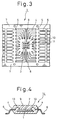
In Fig. 3, a lead frame 1 used for a semiconductor
device of a resin shield type is provided with a die-pad
section 3 for carrying a semiconductor element 2
thereon, inner leads 4 arranged on the periphery of the
die-pad section 3 to be electrically connected to the
semiconductor element 2, dam bars 5 connecting the inner
leads with each other, outer leads 6 extended outward
from the dam bars 5 and so on. The die-pad section 3 is
held by a support bar 8 connected to a pair of rail
sections 7 extending along the respective longitudinal
edges of the lead frame. In this regard, in Fig. 3, a
dotted line shows an area to be resin-shielded.
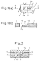
Next, the arrangement of the die-pad section 3 will
be described with reference to Figs. 1(a), 1(b) and 2.
The die-pad section 3 has a plurality of slits 10 in
which a shield resin 9 is to be filled and a plurality
of inserts 11. A proximal end 11a of the insert 11 is
integrally connected to the die-pad section 3, and a
distal end 11b thereof defines a free end to be inserted
into and face the slit 10 and has a thickness smaller
than that of the remainder of the die-pad section 3. The
insert 11 is embedded in the shield resin 9 filled in
the slit 10 to be anchored with each other. In Figs.
1(a) and 1(b), the plurality of slits 10 and inserts 11
are formed to have U-shaped cross-sections, by being
passed through the die-pad section 3, wherein the
inserts 11 have a thickness smaller than that of the
remainder of the die-pad section 3.
The slit 10 and the insert 11 formed in the die-pad
section 3 are made by a punching operation, and the
insert 11 is then pressed, on the side on which the
semiconductor element is to be mounted, to have a
smaller thickness. Although the distal end 11b of the
insert 11 defining a free end is deformed during the
press working of the die-pad section 3, there is no risk
that the die-pad section 3 itself will warp in the
direction to worsen the flatness, because the insert
extends toward the interior of the slit 10. According to
an experiment, it was found that the warping of the die-pad
section 3 could be suppressed to 3 µm or less to
improve the flatness.
Alternatively, the insert 11 in the die-pad section
3 may be formed by a half etching method while using a
mask. Concretely, as shown in Figs. 5(a) to 5(c), resist
layers 16 having different patterns from each other are
formed, respectively, on the side of the die-pad section
3 on which the semiconductor element is to be mounted
and on the side opposite thereto. That is, as shown in
Fig. 5(a), a resist layer 16 having an opening 16a
including the slit 10 and the distal end 11b of the
insert 11 is formed on the side of the die-pad section 3
on which the semiconductor element is to be mounted. As
shown in Fig. 5(b), an opening 16b corresponding to a
shape of the slit 10 is formed on the opposite side.
Under such a condition, when the lead frame 1 is
immersed in an etching liquid, the insert 11 shown in
Fig. 6 is obtained within the slit 10 of the die-pad
section 3, wherein the thickness is reduced solely on
the side on which the semiconductor element is to be
mounted. In this case, no strain is generated in the
die-pad section 3 due to the press working, and the
flatness of the die-pad section 3 is improved.
Accordingly, there is no need for a special
installation for correcting the warp of the die-pad
section 3, whereby the production cost of the lead frame
is reduced.
In this regard, the shape of the slit 10 should not
be limited to a U-shape as described above, but may
include an H-shape as shown in Figs. 7(a) and 7(b), a
quadrant shape as shown in Figs. 8(a) and 8(b) or
another shape.
When the semiconductor device is produced using the
above-mentioned lead frame 1, the semiconductor element
2 is positioned and mounted to the die-pad section 3 of
the lead frame 1 having the slits 10 and the inserts 11
formed in the die-pad section 3 as shown in Fig. 2. In
this case, the die-pad section 3 is coated in advance
with a silver paste 12 used as an adhesive, and the
semiconductor element 2 is mounted thereon via the
silver paste 12. At this time, a gap is defined between
the semiconductor element 2 and the insert 11 which
becomes thinner from the side on which the semiconductor
element is to be mounted.
Then, electrodes of the semiconductor element 2 are
electrically connected to the inner leads 4 by bonding
wires 13. And, as shown in Fig. 4, the semiconductor
element 2 and the inner leads 4 connected thereto are
shielded with resin to complete the semiconductor device
14.
The shield resin 9 not only shields the side of the
die-pad section 3 on which the semiconductor element is
mounted but also flows to the back side of the die-pad
section 3 as shown in Fig. 2 to fill the slit 10,
whereby the insert 11 is embedded in the shield resin 9.
Since the insert 11 is embedded in such a manner in the
shield resin 9 which is hardened thereafter, the
mechanical bonding between the die-pad section 3 and the
shield resin 9 becomes firm and rigid, whereby a
favorable bonding strength is maintained between the
shield resin 9 and the die-pad section 3 against stress
separating them from each other even in after repeated
heat application during an environmental resistance
test.
A comparison of the bonding strength of the die-pad
section in the prior art with that of the die-pad
section in the present invention relative to the shield
resin will be more concretely explained below. As shown
in Figs. 9(a) to 9(c), in the prior art, dimples 15
(Fig. 9(b)) or slits 10 (Fig. 9(c)) are provided in a
flat die-pad section 3 shown in Fig. 9(a) to improve the
bonding strength between the shield resin 9 and the die-pad
section 3. The dimples 15 are provided for the
purpose of increasing the contact area of the die-pad
section 3 with the shield resin 9. Also, the slit 10 is
provided for holding the shield resin therein to
increase the bonding strength.
However, since these countermeasures have no
function of locking the shield resin 9 when stress is
applied to separate the shield resin 9 from the die-pad
section 3, there is a risk of separation of the resin if
the flatness of the die-pad section 3 is impaired due to
the strain in the lead frame 1. In particular, this
problem is more apparent if the dimples 15 are formed on
the die-pad section 3 by press working.
Contrarily, according to the die-pad section 3 of
the semiconductor device 14 of the present invention,
since the shield resin 9 filled in the slits 10 is
hardened while the inserts 11 are embedded therein, the
shield resin 9 is firmly locked to the die-pad section
3, as shown in Fig. 9(a). Therefore, an improved bonding
strength is maintained between the die-pad section 3 and
the shield resin 9 against the thermal stress applied to
the semiconductor device 14. Since a sufficient area of
the die-pad section 3 is obtainable, the heat
dissipation of the semiconductor device is also
facilitated to increase the reliability of the
semiconductor device.
Figs. 10(a) to 10(d) show various layouts of the
slits 10 and the inserts 11 in the die-pad section 3.
The slits 10 and the inserts 11 may be arranged in a
random manner, but are preferably arranged in a cross
shape as shown in Fig. 10(a), in a square shape as shown
in Fig. 10(b), in an X-shape as shown in Fig. 10(c) and
in a diamond shape as shown in Fig. 10(d). In this
connection, to strengthen the locked state of the shield
resin, the inserts 11 formed in the adjacent slits 10
are preferably arranged in different directions such as,
for example, in a zigzag manner.
As described above with reference to the preferred
embodiments, the present invention should not be limited
to the above-mentioned embodiments, but it can include
various changes and modifications without departing from
the spirit of the present invention. For example, the
shape of the slit 10 and the layout on the die-pad 3 may
be optionally variable.
According to the lead frame of the present
invention, since a plurality of slits are formed in the
die-pad section on which a semiconductor element is to
be mounted and each has an insert coupled to the die-pad
section by a proximal end thereof and defining a free
end directed toward the slit at a distal end thereof,
the thickness of the insert being smaller than that of
the remainder of the die-pad section, it is possible to
improve the flatness of the die-pad section when the
slits and the inserts are formed in the die-pad section
by press working or etching. Also, since a special
installation for correcting a warp of the die-pad
section is unnecessary, it is possible to lower the
production cost of the lead frame.
Also, when the semiconductor device is produced
while using the above-mentioned lead frame, the shield
resin filled in the slits of the die-pad section is
hardened while the inserts are embedded therein and
firmly locked to the die-pad section. Therefore, a
favorable bonding strength is maintained against thermal
stress applied to the semiconductor device. The contact
between the die-pad section and the shield resin is
significantly facilitated and a sufficient area of the
die-pad section is obtainable, whereby it is possible to
favorably maintain the heat dissipation of the
semiconductor device to improve the reliability of the
semiconductor device.