EP1073104A2 - Amélioration de la résistance à la rayure par remplissage des espaces entre textures métalliques - Google Patents
Amélioration de la résistance à la rayure par remplissage des espaces entre textures métalliques Download PDFInfo
- Publication number
- EP1073104A2 EP1073104A2 EP00305837A EP00305837A EP1073104A2 EP 1073104 A2 EP1073104 A2 EP 1073104A2 EP 00305837 A EP00305837 A EP 00305837A EP 00305837 A EP00305837 A EP 00305837A EP 1073104 A2 EP1073104 A2 EP 1073104A2
- Authority
- EP
- European Patent Office
- Prior art keywords
- oxide
- layer
- capacitive electrodes
- integrated circuit
- electrodes
- Prior art date
- Legal status (The legal status is an assumption and is not a legal conclusion. Google has not performed a legal analysis and makes no representation as to the accuracy of the status listed.)
- Withdrawn
Links
Images


Classifications
-
- H—ELECTRICITY
- H01—ELECTRIC ELEMENTS
- H01L—SEMICONDUCTOR DEVICES NOT COVERED BY CLASS H10
- H01L23/00—Details of semiconductor or other solid state devices
- H01L23/28—Encapsulations, e.g. encapsulating layers, coatings, e.g. for protection
- H01L23/31—Encapsulations, e.g. encapsulating layers, coatings, e.g. for protection characterised by the arrangement or shape
- H01L23/3157—Partial encapsulation or coating
- H01L23/3192—Multilayer coating
-
- G—PHYSICS
- G06—COMPUTING; CALCULATING OR COUNTING
- G06V—IMAGE OR VIDEO RECOGNITION OR UNDERSTANDING
- G06V40/00—Recognition of biometric, human-related or animal-related patterns in image or video data
- G06V40/10—Human or animal bodies, e.g. vehicle occupants or pedestrians; Body parts, e.g. hands
- G06V40/12—Fingerprints or palmprints
- G06V40/13—Sensors therefor
- G06V40/1329—Protecting the fingerprint sensor against damage caused by the finger
-
- H—ELECTRICITY
- H01—ELECTRIC ELEMENTS
- H01L—SEMICONDUCTOR DEVICES NOT COVERED BY CLASS H10
- H01L23/00—Details of semiconductor or other solid state devices
- H01L23/58—Structural electrical arrangements for semiconductor devices not otherwise provided for, e.g. in combination with batteries
- H01L23/60—Protection against electrostatic charges or discharges, e.g. Faraday shields
-
- H—ELECTRICITY
- H01—ELECTRIC ELEMENTS
- H01L—SEMICONDUCTOR DEVICES NOT COVERED BY CLASS H10
- H01L21/00—Processes or apparatus adapted for the manufacture or treatment of semiconductor or solid state devices or of parts thereof
- H01L21/02—Manufacture or treatment of semiconductor devices or of parts thereof
- H01L21/02104—Forming layers
- H01L21/02107—Forming insulating materials on a substrate
- H01L21/02109—Forming insulating materials on a substrate characterised by the type of layer, e.g. type of material, porous/non-porous, pre-cursors, mixtures or laminates
- H01L21/02112—Forming insulating materials on a substrate characterised by the type of layer, e.g. type of material, porous/non-porous, pre-cursors, mixtures or laminates characterised by the material of the layer
- H01L21/02123—Forming insulating materials on a substrate characterised by the type of layer, e.g. type of material, porous/non-porous, pre-cursors, mixtures or laminates characterised by the material of the layer the material containing silicon
- H01L21/02126—Forming insulating materials on a substrate characterised by the type of layer, e.g. type of material, porous/non-porous, pre-cursors, mixtures or laminates characterised by the material of the layer the material containing silicon the material containing Si, O, and at least one of H, N, C, F, or other non-metal elements, e.g. SiOC, SiOC:H or SiONC
- H01L21/02129—Forming insulating materials on a substrate characterised by the type of layer, e.g. type of material, porous/non-porous, pre-cursors, mixtures or laminates characterised by the material of the layer the material containing silicon the material containing Si, O, and at least one of H, N, C, F, or other non-metal elements, e.g. SiOC, SiOC:H or SiONC the material being boron or phosphorus doped silicon oxides, e.g. BPSG, BSG or PSG
-
- H—ELECTRICITY
- H01—ELECTRIC ELEMENTS
- H01L—SEMICONDUCTOR DEVICES NOT COVERED BY CLASS H10
- H01L21/00—Processes or apparatus adapted for the manufacture or treatment of semiconductor or solid state devices or of parts thereof
- H01L21/02—Manufacture or treatment of semiconductor devices or of parts thereof
- H01L21/02104—Forming layers
- H01L21/02107—Forming insulating materials on a substrate
- H01L21/02109—Forming insulating materials on a substrate characterised by the type of layer, e.g. type of material, porous/non-porous, pre-cursors, mixtures or laminates
- H01L21/02112—Forming insulating materials on a substrate characterised by the type of layer, e.g. type of material, porous/non-porous, pre-cursors, mixtures or laminates characterised by the material of the layer
- H01L21/02123—Forming insulating materials on a substrate characterised by the type of layer, e.g. type of material, porous/non-porous, pre-cursors, mixtures or laminates characterised by the material of the layer the material containing silicon
- H01L21/02126—Forming insulating materials on a substrate characterised by the type of layer, e.g. type of material, porous/non-porous, pre-cursors, mixtures or laminates characterised by the material of the layer the material containing silicon the material containing Si, O, and at least one of H, N, C, F, or other non-metal elements, e.g. SiOC, SiOC:H or SiONC
- H01L21/02134—Forming insulating materials on a substrate characterised by the type of layer, e.g. type of material, porous/non-porous, pre-cursors, mixtures or laminates characterised by the material of the layer the material containing silicon the material containing Si, O, and at least one of H, N, C, F, or other non-metal elements, e.g. SiOC, SiOC:H or SiONC the material comprising hydrogen silsesquioxane, e.g. HSQ
-
- H—ELECTRICITY
- H01—ELECTRIC ELEMENTS
- H01L—SEMICONDUCTOR DEVICES NOT COVERED BY CLASS H10
- H01L21/00—Processes or apparatus adapted for the manufacture or treatment of semiconductor or solid state devices or of parts thereof
- H01L21/02—Manufacture or treatment of semiconductor devices or of parts thereof
- H01L21/02104—Forming layers
- H01L21/02107—Forming insulating materials on a substrate
- H01L21/02109—Forming insulating materials on a substrate characterised by the type of layer, e.g. type of material, porous/non-porous, pre-cursors, mixtures or laminates
- H01L21/022—Forming insulating materials on a substrate characterised by the type of layer, e.g. type of material, porous/non-porous, pre-cursors, mixtures or laminates the layer being a laminate, i.e. composed of sublayers, e.g. stacks of alternating high-k metal oxides
-
- H—ELECTRICITY
- H01—ELECTRIC ELEMENTS
- H01L—SEMICONDUCTOR DEVICES NOT COVERED BY CLASS H10
- H01L21/00—Processes or apparatus adapted for the manufacture or treatment of semiconductor or solid state devices or of parts thereof
- H01L21/02—Manufacture or treatment of semiconductor devices or of parts thereof
- H01L21/04—Manufacture or treatment of semiconductor devices or of parts thereof the devices having at least one potential-jump barrier or surface barrier, e.g. PN junction, depletion layer or carrier concentration layer
- H01L21/18—Manufacture or treatment of semiconductor devices or of parts thereof the devices having at least one potential-jump barrier or surface barrier, e.g. PN junction, depletion layer or carrier concentration layer the devices having semiconductor bodies comprising elements of Group IV of the Periodic System or AIIIBV compounds with or without impurities, e.g. doping materials
- H01L21/30—Treatment of semiconductor bodies using processes or apparatus not provided for in groups H01L21/20 - H01L21/26
- H01L21/31—Treatment of semiconductor bodies using processes or apparatus not provided for in groups H01L21/20 - H01L21/26 to form insulating layers thereon, e.g. for masking or by using photolithographic techniques; After treatment of these layers; Selection of materials for these layers
- H01L21/312—Organic layers, e.g. photoresist
- H01L21/3121—Layers comprising organo-silicon compounds
- H01L21/3122—Layers comprising organo-silicon compounds layers comprising polysiloxane compounds
- H01L21/3124—Layers comprising organo-silicon compounds layers comprising polysiloxane compounds layers comprising hydrogen silsesquioxane
-
- H—ELECTRICITY
- H01—ELECTRIC ELEMENTS
- H01L—SEMICONDUCTOR DEVICES NOT COVERED BY CLASS H10
- H01L2924/00—Indexing scheme for arrangements or methods for connecting or disconnecting semiconductor or solid-state bodies as covered by H01L24/00
- H01L2924/0001—Technical content checked by a classifier
- H01L2924/0002—Not covered by any one of groups H01L24/00, H01L24/00 and H01L2224/00
-
- H—ELECTRICITY
- H01—ELECTRIC ELEMENTS
- H01L—SEMICONDUCTOR DEVICES NOT COVERED BY CLASS H10
- H01L2924/00—Indexing scheme for arrangements or methods for connecting or disconnecting semiconductor or solid-state bodies as covered by H01L24/00
- H01L2924/19—Details of hybrid assemblies other than the semiconductor or other solid state devices to be connected
- H01L2924/1901—Structure
- H01L2924/1904—Component type
- H01L2924/19041—Component type being a capacitor
Definitions
- the present invention relates generally to scratch protection for integrated sensor circuits, and more specifically to improvement of scratch protection in capacitive sensor circuits through planarization of passivation overlying capacitive sensor electrodes.
- Fingerprint acquisition circuits employ arrays of sensors coated with a dielectric onto which the finger is placed with the epidermis in contact with the dielectric. The ridges and grooves on the epidermal layer of the finger are then detected by the sensors, which transmit signals representative of the detected pattern.
- various sensors e.g., resistive, etc.
- capacitive sensors have been found to provide the best performance and security. Since capacitance between two capacitive plates is inversely proportional to the distance between the plates, using the contacting dermal tissue itself as one capacitor plate and the sensor electrode as the other and then determining capacitance for each sensor electrode in the array, it is possible to locate the ridges and grooves of the fingerprint.
- Such capacitive sensors cannot be mechanically protected because physical contact on the surface of the integrated circuit with the finger is necessary.
- some scratch resistance protection for the capacitive sensor electrodes is required to prevent "scratch” damage to the sensor electrodes. Such damage typically results from undue (and unnecessary) pressure on the surface of the integrated circuit, alone or in combination with some sharp edge or protrusion such as a callous or scar, fingernail, rings, dust or dirt particle, etc.
- SiC silicon carbide
- Passivation for capacitive sensor circuits which overlies the capacitive sensor electrodes and is normally conformal to the electrodes and the underlying interlevel dielectric, is planarized by forming a layer of flowable oxide over the electrodes before forming the passivation.
- the flowable oxide which is preferably very thin over the electrodes to minimize loss of sensitivity, provides a substantially planar upper surface, so that passivation formed on the flowable oxide is also substantially planar.
- a deposited oxide planarized by chemical mechanical polishing may be employed to planarize the surface on which a passivation stack is formed. The planarized passivation provides markedly improved scratch resistance.
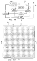
- Figure 1A depicts a block diagram of the sensor circuit 102 , which is formed as an integrated circuit on a single die.
- the sensor circuit 102 and its operation are described more fully in commonly assigned, copending application serial no. 09/040,261, entitled “CAPACITIVE DISTANCE SENSOR” and filed May 9, 1998, which is incorporated herein by reference.
- sensor circuit 102 relevant to the present invention include an array 104 of capacitive sensors for fingerprint acquisition by sensing distances between capacitive electrodes within the sensor array 104 and ridges and grooves on a finger placed in contact with sensor array 104 .
- Sensor circuit 102 also includes signal lines 106 and 108 and output bus 110 .
- Signal line 106 connects I 2 C interface and control device 104 , which provides a bidirectional communication protocol enabling sensor circuit 102 to communicate with a controller such as a microcontroller, with controller circuitry (not shown) external to sensor circuit 102 .
- Signal line 108 is a synchronization line coupling sensor array 104 to the external controller circuit, providing synchronization signals allowing detected voltages representative of the capacitive value of individual capacitive electrodes within sensor array 104 , and therefore representative of the distance between the capacitive electrode and the portion of the epidermal layer contacting sensor array 104 in the region of the capacitive electrode, to be properly interpreted by the external controller.
- Output bus 110 coupling an analog-to-digital (A/D) converter 114 to the external controller.
- A/D converter 114 processes analog voltage measurements received from sensor array 104 and generates digital representations recognized by the external controller as distance measurements of the analog measured voltages from individual capacitive electrodes within sensor array 104 .
- A/D converter 114 transmits these digital signals to the external controller on output bus 110 .
- Figure 1B is a pictorial representation of the "front" side of sensor circuit 102 ; that is, Figure 1B depicts the major surface of the die 116 on which the active devices constituting sensor circuit 102 are formed.
- Sensor array 104 is located on the front side of die 116 and includes a plurality of cells 118 , each containing one or more capacitive electrodes.
- Sensor array 104 in the exemplary embodiment contains square cells approximately 45-50 ⁇ m on a side, forming a 250 X 350 array of contiguous cells 118 within sensor array 104 .
- Sensor array 104 is covered by a passivation material overlying the capacitive electrodes within each cell 118 .
- Other active devices required to form sensor circuit 102 are formed below the capacitive electrodes.
- FIG. 2A illustrates sensor circuit passivation in accordance with the known art.
- Sensor circuit 102 includes metal electrodes 202 for the capacitive sensors overlying an interlevel dielectric 204 , such as an oxide.
- Passivation formed over capacitive metal electrodes 202 includes phosphosilicate glass (PSG) layer 206 , silicon nitride (SiN) layer 208 , and silicon carbide (SiC) layer 210 , which together form the passivation for sensor circuit 102 .
- the passivation layers 206 , 208 and 210 are conventionally formed conformally over electrodes 202 and dielectric 204 . This structure has been found to provide less than completely satisfactory scratch resistance, even when tungsten electrostatic discharge (ESD) protection patterns and/or capacitive electrodes are employed.
- FIG. 2B illustrates sensor circuit passivation in accordance with the present invention. Scratch resistance is improved by filling the spaces between the metal electrodes 202 to prevent these electrodes from crashing under pressure.
- the sensitivity of the capacitive cells within sensor circuit 102 should not be degraded, which means that the capacitance should not be significantly reduced by additional dielectric thickness between the capacitive electrodes 202 and the finger or by introduction of materials with a high dielectric constant.
- a hydrogen silsesquioxane (HSQ) layer 212 is formed over the interlevel dielectric 204 and capacitive metal electrodes 202 before forming the passivation.
- HSQ hydrogen silsesquioxane
- HSQ (also referred to as "flowable oxide”) layer 212 may be formed according to known processes and exhibits a very high planarization, greater than 90% planar at spacings of 5 ⁇ m or less. HSQ also has excellent gap filling capabilities, down to 0.1 ⁇ m spaces, and a low dielectric constant (less than 3). Thus HSQ layer 212 should not significantly degrade the sensitivity of sensor circuit 102 .
- HSQ layer 212 is formed very thin over capacitive electrodes 202 , with less than the thickness of capacitive electrodes 202 (approximately 1 ⁇ m thick) overlying the capacitive electrodes 202 . The thickness of HSQ layer 212 in regions adjacent to capacitive electrodes 202 is thus preferably only slightly thicker than the capacitive electrodes 202 themselves.
- HSQ layer 212 provides a substantially planar upper surface, on which is formed the passivation: PSG layer 206 to a thickness of approximately 5,000 ⁇ ; SiN layer 208 to a thickness of approximately 5,000 ⁇ ; and SiC layer 210 to a thickness of approximately 2,500 ⁇ .
- PSG layer 206 may be formed before HSQ layer 212 , but is preferably formed over HSQ layer 212 since the interface between HSQ and nitride is weaker.
- oxide may be deposited in lieu of (or in addition to) HSQ layer 212 , and planarized utilizing a planarizing etch-back, such as chemical mechanical polishing (CMP).
- Figure 2C illustrates sensor circuit passivation in accordance with an alternative embodiment of the present invention, in which SiC layer 210 is omitted.
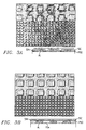
- test structures passivated with conformal PSG, SiN and SiC layers in accordance with the known art were subject to a 2 N force by a 1 mm steel stylus are seen to be damaged.
- Sensor circuits passivated in this manner are known to scratch easily, and may be rendered inoperative by a 1 N force applied by a 0.5 mm diamond pin.
- Figures 3B and 3C illustrate the effect of the same 2 N force applied by a 1 mm steel stylus on test structures passivated with a planarizing layer of flowable oxide in accordance with the present invention.
- Figure 3B illustrates the result when a SiC layer is employed, while Figure 3C illustrates the result without an SiC layer. As shown, no damage is detectable.
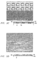
- Figures 3D through 3F illustrate similar testing as that for Figures 3A through 3C , but with a 5 N force applied by the 1 mm steel stylus. Again, the test structures passivated in the conventional manner were destroyed, as shown in Figure 3D . Test structures passivated with a planarizing FOX layer exhibited no appreciable damage when a silicon carbide layer was employed, as shown in Figure 3E , and only very minimal damage without the silicon carbide layer, as shown in Figure 3F .
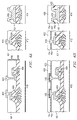
- FIG. 4A through 4F a series of cross-sections for a process of fabricating a sensor circuit in accordance with a preferred embodiment of the present invention are illustrated.
- the process begins with the sensor circuit fabricated to the point of having formed capacitive electrodes 402 connected to underlying conductive polysilicon structures 404 , which may be gate electrodes, source/drain contacts, or interconnects, through an interlevel dielectric 406 and a lower dielectric layer 408 .
- Cross-sections from the sensor array area 410 , the peripheral area 412 , and the pad area 414 of the sensor circuit are depicted.
- Contacts 416 for ESD protection lines and die contact pads 418 are formed within the peripheral area 412 and the pad area 414 , respectively.
- a flowable oxide layer 420 and a PSG layer 422 are then formed over all areas 410 , 412 , and 414 , as shown in Figure 4B .
- PSG layer 422 is formed beneath flowable oxide 420 , although the opposite order is preferred for the reasons described above.
- Vias 424 for the connections to ESD protection lines are then etched as illustrated in Figure 4C , and silicon nitride layer 426 and silicon carbide layer 428 are deposited and patterned for the ESD protection grid as shown in Figure 4D .
- a tungsten layer is then formed and etched back to form ESD protection lines and connections 430 as illustrated in Figure 4E , and an opening to pad 418 is etched as shown in Figure 4F .
- the present invention improves scratch resistance for a capacitive sensor circuit simply by planarizing the passivation, without significantly diminishing the sensitivity of the sensor circuit.
- the spaces between capacitive electrodes at the surface of the sensor circuit, immediately below the passivation, are filled with flowable oxide, with only a very thin layer of flowable oxide formed over the capacitive electrodes themselves, resulting in a planar surface for formation of the passivation layers.
- the planarized passivation provides uniform boundaries for force applied to the surface of the sensor circuit, substantially improving scratch resistance for the circuit.
Landscapes
- Engineering & Computer Science (AREA)
- Power Engineering (AREA)
- General Physics & Mathematics (AREA)
- Physics & Mathematics (AREA)
- Condensed Matter Physics & Semiconductors (AREA)
- Computer Hardware Design (AREA)
- Microelectronics & Electronic Packaging (AREA)
- Human Computer Interaction (AREA)
- Multimedia (AREA)
- Theoretical Computer Science (AREA)
- Measurement Of Length, Angles, Or The Like Using Electric Or Magnetic Means (AREA)
- Image Input (AREA)
- Semiconductor Integrated Circuits (AREA)
- Formation Of Insulating Films (AREA)
Applications Claiming Priority (2)
| Application Number | Priority Date | Filing Date | Title |
|---|---|---|---|
| US09/364,307 US6603192B2 (en) | 1999-07-30 | 1999-07-30 | Scratch resistance improvement by filling metal gaps |
| US364307 | 1999-07-30 |
Publications (2)
| Publication Number | Publication Date |
|---|---|
| EP1073104A2 true EP1073104A2 (fr) | 2001-01-31 |
| EP1073104A3 EP1073104A3 (fr) | 2001-08-01 |
Family
ID=23433930
Family Applications (1)
| Application Number | Title | Priority Date | Filing Date |
|---|---|---|---|
| EP00305837A Withdrawn EP1073104A3 (fr) | 1999-07-30 | 2000-07-12 | Amélioration de la résistance à la rayure par remplissage des espaces entre textures métalliques |
Country Status (2)
| Country | Link |
|---|---|
| US (1) | US6603192B2 (fr) |
| EP (1) | EP1073104A3 (fr) |
Cited By (2)
| Publication number | Priority date | Publication date | Assignee | Title |
|---|---|---|---|---|
| WO2016119915A1 (fr) * | 2015-01-28 | 2016-08-04 | Siltectra Gmbh | Protection d'écran transparente et très stable |
| US10304738B2 (en) | 2013-05-03 | 2019-05-28 | Siltectra | Method and device for the production of wafers with a pre-defined break initiation point |
Families Citing this family (5)
| Publication number | Priority date | Publication date | Assignee | Title |
|---|---|---|---|---|
| US6423995B1 (en) * | 1999-07-26 | 2002-07-23 | Stmicroelectronics, Inc. | Scratch protection for direct contact sensors |
| US6900644B2 (en) * | 2003-05-06 | 2005-05-31 | Ligh Tuning Tech. Inc. | Capacitive fingerprint sensor against ESD damage and contamination interference |
| US7799276B2 (en) * | 2003-10-27 | 2010-09-21 | Michigan Molecular Institute | Functionalized particles for composite sensors |
| US7071708B2 (en) * | 2004-04-16 | 2006-07-04 | Lightuning Tech. Inc. | Chip-type sensor against ESD and stress damages and contamination interference |
| CN109742091B (zh) * | 2019-01-10 | 2021-08-31 | 京东方科技集团股份有限公司 | 显示基板及其制备方法、显示装置 |
Citations (6)
| Publication number | Priority date | Publication date | Assignee | Title |
|---|---|---|---|---|
| US4872947A (en) * | 1986-12-19 | 1989-10-10 | Applied Materials, Inc. | CVD of silicon oxide using TEOS decomposition and in-situ planarization process |
| EP0789334A2 (fr) * | 1996-01-26 | 1997-08-13 | Harris Corporation | Dispositif de circuit intégré à ouverture exposant une puce de circuit intégré et procédés associés |
| WO2000003345A1 (fr) * | 1998-07-09 | 2000-01-20 | Infineon Technologies Ag | Composant semi-conducteur presentant une passivation |
| EP1017009A2 (fr) * | 1998-12-30 | 2000-07-05 | STMicroelectronics, Inc. | Appareil et méthode pour mettre en contact une couche conductive d'un capteur |
| EP1018698A2 (fr) * | 1998-12-30 | 2000-07-12 | STMicroelectronics, Inc. | Dissipation de charge statique pour une surface de circuit active |
| WO2001006448A1 (fr) * | 1999-07-14 | 2001-01-25 | Veridicom, Inc. | Detecteur a circuits integres tres robuste et procede de fabrication dudit detecteur |
Family Cites Families (5)
| Publication number | Priority date | Publication date | Assignee | Title |
|---|---|---|---|---|
| US4353056A (en) | 1980-06-05 | 1982-10-05 | Siemens Corporation | Capacitive fingerprint sensor |
| CA1169022A (fr) * | 1982-04-19 | 1984-06-12 | Kevin Duncan | Methode planar pour circuits integres |
| GB2244164A (en) | 1990-05-18 | 1991-11-20 | Philips Electronic Associated | Fingerprint sensing |
| US6091082A (en) * | 1998-02-17 | 2000-07-18 | Stmicroelectronics, Inc. | Electrostatic discharge protection for integrated circuit sensor passivation |
| US6423995B1 (en) * | 1999-07-26 | 2002-07-23 | Stmicroelectronics, Inc. | Scratch protection for direct contact sensors |
-
1999
- 1999-07-30 US US09/364,307 patent/US6603192B2/en not_active Expired - Lifetime
-
2000
- 2000-07-12 EP EP00305837A patent/EP1073104A3/fr not_active Withdrawn
Patent Citations (6)
| Publication number | Priority date | Publication date | Assignee | Title |
|---|---|---|---|---|
| US4872947A (en) * | 1986-12-19 | 1989-10-10 | Applied Materials, Inc. | CVD of silicon oxide using TEOS decomposition and in-situ planarization process |
| EP0789334A2 (fr) * | 1996-01-26 | 1997-08-13 | Harris Corporation | Dispositif de circuit intégré à ouverture exposant une puce de circuit intégré et procédés associés |
| WO2000003345A1 (fr) * | 1998-07-09 | 2000-01-20 | Infineon Technologies Ag | Composant semi-conducteur presentant une passivation |
| EP1017009A2 (fr) * | 1998-12-30 | 2000-07-05 | STMicroelectronics, Inc. | Appareil et méthode pour mettre en contact une couche conductive d'un capteur |
| EP1018698A2 (fr) * | 1998-12-30 | 2000-07-12 | STMicroelectronics, Inc. | Dissipation de charge statique pour une surface de circuit active |
| WO2001006448A1 (fr) * | 1999-07-14 | 2001-01-25 | Veridicom, Inc. | Detecteur a circuits integres tres robuste et procede de fabrication dudit detecteur |
Cited By (2)
| Publication number | Priority date | Publication date | Assignee | Title |
|---|---|---|---|---|
| US10304738B2 (en) | 2013-05-03 | 2019-05-28 | Siltectra | Method and device for the production of wafers with a pre-defined break initiation point |
| WO2016119915A1 (fr) * | 2015-01-28 | 2016-08-04 | Siltectra Gmbh | Protection d'écran transparente et très stable |
Also Published As
| Publication number | Publication date |
|---|---|
| US6603192B2 (en) | 2003-08-05 |
| US20030071287A1 (en) | 2003-04-17 |
| EP1073104A3 (fr) | 2001-08-01 |
Similar Documents
| Publication | Publication Date | Title |
|---|---|---|
| US8633525B2 (en) | Scratch protection for direct contact sensors | |
| US6740945B2 (en) | Apparatus and method for contacting a conductive layer | |
| EP1256899B1 (fr) | Détecteur d'empreintes digitales avec surface résistante aux égratignures et grille encastrée de protection contre les décharges électrostatiques | |
| EP0940652B1 (fr) | Capteur de reconnaissance de formes de surfaces et son procédé de fabrication | |
| US7339204B2 (en) | Backside contact for touchchip | |
| US6737329B2 (en) | Static charge dissipation pads for sensors | |
| US20030107097A1 (en) | Ultra-rugged biometric I.C. sensor and method of making the same | |
| US6686546B2 (en) | Static charge dissipation for an active circuit surface | |
| EP2332095B1 (fr) | Capteur de surface | |
| US6501142B2 (en) | Topographical electrostatic protection grid for sensors | |
| US6664612B2 (en) | Semiconductor component having double passivating layers formed of two passivating layers of different dielectric materials | |
| US6330145B1 (en) | Apparatus and method for contacting a sensor conductive layer | |
| EP1187056A2 (fr) | Détection capacitive d'un doigt dans un capteur des empreintes digitales | |
| US6603192B2 (en) | Scratch resistance improvement by filling metal gaps | |
| US20040070407A1 (en) | Fingerprint detector with improved sensing surface layer | |
| JP3371095B2 (ja) | 表面形状認識用センサ |
Legal Events
| Date | Code | Title | Description |
|---|---|---|---|
| PUAI | Public reference made under article 153(3) epc to a published international application that has entered the european phase |
Free format text: ORIGINAL CODE: 0009012 |
|
| AK | Designated contracting states |
Kind code of ref document: A2 Designated state(s): DE FR GB IT |
|
| AX | Request for extension of the european patent |
Free format text: AL;LT;LV;MK;RO;SI |
|
| PUAL | Search report despatched |
Free format text: ORIGINAL CODE: 0009013 |
|
| AK | Designated contracting states |
Kind code of ref document: A3 Designated state(s): AT BE CH CY DE DK ES FI FR GB GR IE IT LI LU MC NL PT SE |
|
| AX | Request for extension of the european patent |
Free format text: AL;LT;LV;MK;RO;SI |
|
| RIC1 | Information provided on ipc code assigned before grant |
Free format text: 7G 06K 9/00 A, 7H 01L 23/64 B, 7H 01L 23/29 B, 7H 01L 23/31 B, 7H 01L 21/3105 B, 7H 01L 21/314 B, 7H 01L 21/56 B |
|
| 17P | Request for examination filed |
Effective date: 20020110 |
|
| AKX | Designation fees paid |
Free format text: DE FR GB IT |
|
| 17Q | First examination report despatched |
Effective date: 20020515 |
|
| 17Q | First examination report despatched |
Effective date: 20020515 |
|
| GRAP | Despatch of communication of intention to grant a patent |
Free format text: ORIGINAL CODE: EPIDOSNIGR1 |
|
| STAA | Information on the status of an ep patent application or granted ep patent |
Free format text: STATUS: THE APPLICATION IS DEEMED TO BE WITHDRAWN |
|
| 18D | Application deemed to be withdrawn |
Effective date: 20080930 |