EP1071155A2 - Small-sized cylindrical waveguide bend having low reflection characteristic - Google Patents
Small-sized cylindrical waveguide bend having low reflection characteristic Download PDFInfo
- Publication number
- EP1071155A2 EP1071155A2 EP00305783A EP00305783A EP1071155A2 EP 1071155 A2 EP1071155 A2 EP 1071155A2 EP 00305783 A EP00305783 A EP 00305783A EP 00305783 A EP00305783 A EP 00305783A EP 1071155 A2 EP1071155 A2 EP 1071155A2
- Authority
- EP
- European Patent Office
- Prior art keywords
- cavity
- waveguide
- wall portion
- cavities
- cylindrical
- Prior art date
- Legal status (The legal status is an assumption and is not a legal conclusion. Google has not performed a legal analysis and makes no representation as to the accuracy of the status listed.)
- Withdrawn
Links
Images


Classifications
-
- H—ELECTRICITY
- H01—ELECTRIC ELEMENTS
- H01Q—ANTENNAS, i.e. RADIO AERIALS
- H01Q13/00—Waveguide horns or mouths; Slot antennas; Leaky-waveguide antennas; Equivalent structures causing radiation along the transmission path of a guided wave
- H01Q13/02—Waveguide horns
- H01Q13/025—Multimode horn antennas; Horns using higher mode of propagation
- H01Q13/0258—Orthomode horns
-
- H—ELECTRICITY
- H01—ELECTRIC ELEMENTS
- H01P—WAVEGUIDES; RESONATORS, LINES, OR OTHER DEVICES OF THE WAVEGUIDE TYPE
- H01P1/00—Auxiliary devices
- H01P1/02—Bends; Corners; Twists
-
- H—ELECTRICITY
- H01—ELECTRIC ELEMENTS
- H01P—WAVEGUIDES; RESONATORS, LINES, OR OTHER DEVICES OF THE WAVEGUIDE TYPE
- H01P1/00—Auxiliary devices
- H01P1/16—Auxiliary devices for mode selection, e.g. mode suppression or mode promotion; for mode conversion
- H01P1/161—Auxiliary devices for mode selection, e.g. mode suppression or mode promotion; for mode conversion sustaining two independent orthogonal modes, e.g. orthomode transducer
Definitions
- the present invention relates to a cylindrical waveguide to be used, for example, as a satellite broadcast transmitting and receiving antenna for the transmission and reception of a polarized wave.
- FIG. 8 is an exploded perspective view of the conventional converter
- Fig. 9 is an explanatory diagram for explaining a bent portion of a cavity in the cylindrical waveguide of the conventional converter.
- a body member 31 formed by aluminum or zinc die casting comprises a cylindrical waveguide 32 for introducing a polarized wave and a housing 41 for receiving a circuit portion therein, the cylindrical waveguide 32 and the housing 41 being formed integrally with each other.
- the cylindrical waveguide 32 has a first cylindrical waveguide portion 34 having a horn portion 33 for introducing a polarized wave, a second cylindrical waveguide portion 35 disposed perpendicularly to the first waveguide portion 34, and a cylindrical connection 36 which connects the first and second waveguide portions 34, 35 with each other and which is bent 90°.
- a first cavity 37 Centrally and axially of the first waveguide portion 34 is formed a first cavity 37 which is straight, and also formed centrally and axially of the second waveguide portion 35 is a second cavity 38 which is straight.
- the first and second cavities 37, 38 are connected with each other through a 90°-bent cavity 39 which is formed in the connection 36 to form a cavity 40.
- a first opening 40a which opens one end of the cavity 40.
- the opposite end side of the cavity 40 is also open.
- the housing 41 which is formed of the same material as the cylindrical waveguide 32, has a bottom wall portion 41a, a side wall portion 41b which is formed upright so as to enclose the bottom wall portion 41a, and a receptacle portion 41c which is open above the side wall portion 41b and which is enclosed with the side wall portion 41b.
- a second opening 41d Near one end side of the bottom wall portion 41a is formed a second opening 41d which is an opposite end-side opening of the cavity 40.
- annular earth electrodes 43 On both upper and lower sides of a single rectangular circuit board 42 constituted by an insulating board are formed annular earth electrodes 43 as soldered layers each having about the same diameter as the second opening portion 41d. A large number of through holes 43a extending vertically through the circuit board 42 are formed in both upper- and lower-side earth electrodes 43 to connect the earth electrodes with each other.
- a first probe 44 for catching a vertically polarized wave is formed by a conductive pattern longitudinally of the circuit board 42 from near the center of the earth electrode 43 formed on the upper side of the circuit board.
- an L-shaped, second probe 45 by a conductive pattern to catch a horizontally polarized wave.
- One ends of the first and second probes 44, 45 are connected to an electric circuit (not shown) formed on the upper surface of the circuit board 42.
- the circuit board 42 is placed on a stepped portion located near the bottom wall portion 41a out of plural stepped portions (not shown) formed inside the housing 41 and is fixed to the housing by a suitable means. At this time, the earth electrode 43 formed on the lower side of the circuit board is grounded to the bottom wall portion 41a while surrounding the second opening 41d formed in the housing 41.
- a generally square, bottomed, metallic case 46 is attached to the circuit board 42 so as to cover the earth electrode 43 formed on the upper side of the circuit board 42, by a suitable means such as the use of screws.
- An inside bottom (not shown) of the metallic case 46 functions as a short-circuit surface for the first and second probes 44, 45.
- a cover 47 constituted by a single rectangular metallic plate is placed on a stepped portion (not shown) located on a remote side from the bottom wall portion 41a of the housing 41 and is fixed by a suitable means.
- the receptacle portion 41c of the housing 41 is sealed hermetically and the interior thereof is held in an electrically shielded state.
- the first and second cavities 37, 38 are each formed at a diameter of D1, and on the innermost side of the cavity 40 when seen sideways of the body member 31, the cavities 37 and 38 are constituted by an innermost wall portion 37a of the fist cavity 37, an innermost wall portion 38a of the second cavity 38, and an inner bent portion 39a as an innermost wall portion of the cavity 39 in the connection 36 which connects the first and second cavities 37, 38 with each other.
- the first and second cavities 37, 38 are constituted by an outermost inner wall portion 37b of the first cavity 37, an outermost inner wall portion 38b of the second cavity 38, and an outer bent portion 39b as an outermost inner wall portion of the cavity 39 in the connection 36.
- the inner bent portion 39a has a quadrant circumference described with a radius of R2 which is three times as long as the diameter D1 from a central position C4, the central position C4 lying on a 45° line at an intersecting point of an extension line X1 of the innermost wall portion 37a of the first cavity 37 and an extension line Y1 of the innermost wall portion 38a of the second cavity 38.
- the innermost wall portions 37a and 38a of the first and second cavities 37, 38 are connected together at the radius R2.
- the outer bent portion 39b has a quadrant circumference described at a radius of R3 which is four times as long as the diameter D1 also from the central position C4.
- the outermost inner wall portions 37b and 38b are connected with each other at the radius R3.
- the central position of the radius R2 of the inner bent portion 39a of the cavity portion 39 in the connection 36 and the radius R3 of the outer bent portion 39b of the cavity 39 are the same and the radii R2 and R3 are respectively three and four times as long as the diameter D1, so that the cavity 39 is large in the directions of the extension lines X1 and Y1, with consequent increase in size of the connection 36, thus giving rise to the problem that the cylindrical waveguide 32 becomes larger in size.
- a cylindrical waveguide comprising a first waveguide portion having a cylindrical cavity, a second waveguide portion disposed perpendicularly to the first waveguide portion and having a cylindrical cavity, and a connection connecting the first and second waveguide portions with each other and having a bent cylindrical cavity, wherein an inner bent portion of an inner wall portion in the cavity of the connection connects the cavities of the first and second waveguide portions with each other on a bent right-angle side and at a first radius from a first central position, while an outer bent portion of the inner wall portion in the cavity of the connection connects the cavities of the first and second waveguide portions with each other on the bent right-angle side and at a second radius from a second central position, and the inner bent portion connects the cavities of the first and second waveguide portions with each other in a range of not larger than one-fourth of the diameter of the cavities on each of an extension line of the innermost wall portion in the cavity of the first
- the radius from the first central position is set zero, and the cavities of the first and second waveguide portions are connected perpendicularly to each other by the inner bent portion of the inner wall portion in the cavity of the connection.
- the radius from the second central position is set 1.5 to 5 times as large as the cavity diameter, and the cavities of the first and second waveguide poritons are connected with each other by the outer bent portion of the inner wall portion in the cavity of the connection.
- the first and second central positions lie on a 45° line which bisects the right-angled bent side.
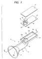
- a body member 1 which is formed by aluminum or zinc die casting, comprises a cylindrical waveguide 2 for introducing a polarized wave and a housing 11 for receiving a circuit portion therein.
- the cylindrical waveguide 2 comprises a first cylindrical waveguide portion 4 having a horn portion 3 for introducing a polarized wave, a second cylindrical waveguide portion 5 disposed perpendicularly to the first waveguide portion 4, and a 90°-bent cylindrical connection 6 which connects the first and second waveguide portions 3, 5 with each other.
- a first cavity 7 Centrally and axially of the first waveguide portion 4 is formed a first cavity 7 which is straight.
- a second cavity 8, which is also straight, is formed centrally and axially of the second waveguide portion 5.
- the first and second cavities 7, 8 are connected to a 90°-bent cavity 9 formed in the connection 6 to form a cavity 10.
- a first opening 10a as an opening at one end of the cavity 10.
- the opposite end side of the cavity 10 is also open.
- the housing 11 which is formed of the same material as the material of the cylindrical waveguide 2, comprises a bottom wall portion 11a, a side wall portion 11b formed upright so as to enclose the bottom wall portion 11a, and a receptacle portion 11c which is enclosed with the side wall portion 11b so as to be open above the side wall portion. Inside the side wall portion 11b are formed a plurality of stepped portions 11d. Near one end side of the bottom wall portion 11a is formed a second opening 11e as an opening on the opposite end side of the cavity 10.
- annular earth electrodes 13 On both upper and lower sides of a single rectangular circuit board 12 constituted by an insulating board are formed annular earth electrodes 13 of about the same diameter as the diameter of the second opening 11e, the earth electrodes 13 being each formed by a soldered layer. A large number of through holes 13a are formed in the upper and lower earth electrodes 13 to as to extend vertically through the circuit board 12, thereby connecting the earth electrodes with each other.
- a first probe 14 for catching a vertically polarized wave is formed by a conductive pattern longitudinally of the circuit board 12 from near the center of the earth electrode formed on the upper side of the circuit board.
- an L-shaped, second probe 15 by a conductive pattern for catching a horizontally polarized wave.
- One ends of the first and second probes 14, 15 are connected to an electric circuit (not shown) formed on the upper side of the circuit board 12.
- the circuit board 12 is placed on a stepped portion located near the bottom wall portion 11a of the housing 11 out of plural stepped portions 11d formed inside the housing and is fixed to the housing by a suitable means. At this time, the earth electrode 13 formed on the lower side of the circuit board is grounded to the bottom wall portion 11a in a surrounding relation to the second opening 11e.
- a generally square, bottomed, metallic case 16 is mounted to the circuit board 12 so as to cover the earth electrode 13 formed on the upper side of the circuit board, by a suitable means such as the use of screws.
- An inner bottom 16a of the metallic case 16 functions as a short-circuit surface for the first and second probes 14, 15.
- the receptacle portion 11c of the housing 11 is hermetically sealed and the interior thereof is shielded electrically.
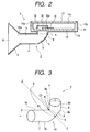
- the first and second cavities 7, 8 are each formed at a diameter of D.
- the first and second cavities 7, 8 are formed by an innermost wall portion 7a of the first cavity 7, an innermost wall portion 8a of the second cavity 8, an inner bent portion 9a as an innermost wall portion of the cavity 9 in the connection 6 which connects the innermost wall portions 7a and 8a with each other
- the first and second cavities 7, 8 are formed by an outermost inner wall portion 7b of the first cavity 7, an outermost inner wall portion 8b of the second cavity 3, and an outer bent portion 9b as an outermost inner wall portion of the cavity 9 in the connection 6 which connects the outermost inner wall portions 7b and 8b with each other.
- the inner bent portion 9a as the innermost wall portion in the cavity 9 of the connection 6 has a quadrant circumference of a first radius R at a first central position C1 on a 45° line Z at an intersecting point K of an extension line X of the inner wall portion 7a in the first cavity 7 and an extension line Y of the inner wall portion 8a in the second cavity 8.
- the inner wall portions 7a and 8a of the first and second cavities 7, 8 are connected with each other.
- the inner bent portion 9a in the cavity 9 connects the inner wall portion 7a of the first cavity 7 and the inner wall portion 8a of the second cavity 8 with each other at a first connection point p and a second connection point p1 lying at one-fourth positions of the diameter D on the extension lines X and Y, respectively, from the intersecting point K of both extension lines.
- the first central position C1 in the above first embodiment is displaced to the outer bent portion 9b side of the cavity 9 on the line Z and the position of the intersecting point K is made a central position C0. That is, the first radius R of the inner bent portion 9a in the cavity 9 is made zero and the first central position C1 is set at the intersecting point K of the extension line X of the inner wall portion 7a in the first cavity 7 and the extension line Y of the inner wall portion 8a in the second cavity 8.
- the innermost wall portions 7a and 8a of the cavities 7 and 8 in the first and second waveguide portions 4, 5 are directly connected perpendicularly to each other.
- the first central position C1 is displaced so as to increase the radius R, allowing the first radius R of the inner bent portion 9a in the cavity 9 to become infinite, and the first central position is set at C2.
- the inner bent portion 9a of the cavity 9 is in the form of a line which substantially intersects the line Z perpendicularly, and connects the innermost wall portion 7a of the first cavity 7 and the innermost wall portion 8a of the second cavity with each other at the first and second connection points p, p1.
- the inner bent portion 9a of the innermost wall portion in the cavity 9 of the connection 6 connects the innermost wall portion 7a of the first cavity 7 and the innermost wall portion 8a of the second cavity 8 with each other within the range of one-fourth of the diameter D on the extension lines X and Y from the intersection point K of the extension line X of the innermost wall portion 7a and the extension line Y of the innermost wall portion 8a and within the range of a triangle formed by connecting the first and second connection points p, p1 and positioned at a corner portion.
- the outermost inner wall portion 9b in the cavity 9 of the connection 6 is in the form of a circumference of radius R1 from the second central position A which lies on the 45° line Z at the intersecting point K of the extension line X of the innermost wall portion 7a in the first cavity 7 and the extension line Y of the innermost wall portion 8a in the second cavity 8.
- the radius R1 is 1.5 to 5 times as large as the diameter D.
- the outer bent portion 9b in the cavity 9 connects the outermost inner wall portion 7b in the first cavity 7 and the outermost inner wall portion 8b in the second cavity 8 with each other.
- the present invention is not limited to the above embodiments.
- the first central position C1 may be established independently of the second central position A, and both central positions C1 and A need not lie on the 45° line Z.
- the cylindrical waveguide 2 according to the present invention may be applied to not only a converter for reception but also a converter for transmission.
- the cavities in the first and second waveguide portions are connected with each other within the range of not larger than one-fourth of the cavity diameter on each of an extension line of the innermost wall portion in the cavity of the first waveguide portion and an extension line of the innermost wall portion in the cavity of the second waveguide portion and from an intersecting point of both extension lines. Therefore, the connection can be formed small and it is possible to provide a small-sized cylindrical waveguide. Besides, since the second central position can be established independently of the first central position, the radius of the outer bent portion from the second central position can be set freely so as to afford a low reflection characteristic without affecting the reduction of size. In other words, it is possible to provide a small-sized cylindrical waveguide while attaining a low reflection characteristic.
- the radius from the first central position is set zero and the cavities of the first and second waveguide portions are connected perpendicularly to each other by the inner bent portion of the inner wall portion in the cavity of the connection, not only the cavity in the connection of the cylindrical waveguide but also the connection itself becomes smaller in size, thus permitting the provision of a cylindrical waveguide smaller in size.
- the cavities in the first and second waveguide portions are connected perpendicularly to each other, the structure of a mold to be used for molding the body member becomes simpler and a cylindrical waveguide superior in mass-productivity can be provided at a lower cost.
- the radius from the second central position is set 1.5 t 5 times as large as the cavity diameter and the cavities in the first and second waveguide portions are connected together by the outer bent portion of the inner wall portion in the cavity of the connection, the curvature of the outer bent portion of the inner wall portion in the cavity of the connection can be set in a range capable of affording a good low reflection characteristic, thus making it possible to provide a highly reliable, cylindrical waveguide.
- the mold structure becomes still simpler and it is possible to provide a cylindrical waveguide superior in mass-productivity at a lower cost.
Landscapes
- Waveguide Connection Structure (AREA)
- Optical Integrated Circuits (AREA)
- Waveguides (AREA)
- Optical Fibers, Optical Fiber Cores, And Optical Fiber Bundles (AREA)
- Non-Reversible Transmitting Devices (AREA)
Abstract
Description
Claims (4)
- A cylindrical waveguide comprising:a first waveguide portion having a cylindrical cavity;a second waveguide portion disposed perpendicularly to the first waveguide portion and having a cylindrical cavity; anda connection connecting the first and second waveguide portions with each other and having a bent cylindrical cavity,
wherein an inner bent portion of an inner wall portion in the cavity of the connection connects the cavities of the first and second waveguide portions with each other on a bent right-angle side and at a first radius from a first central position, while an outer bent portion of the inner wall portion in the cavity of the connection connects the cavities of the first and second waveguide portions with each other on the bent right-angle side and at a second radius from a second central position, and the inner bent portion connects the cavities of the first and second waveguide portions with each other in a range of not larger than one-fourth of the diameter of the cavities on each of an extension line of the innermost wall portion in the cavity of the first waveguide portion and an extension line of the innermost wall portion in the cavity of the second waveguide portion, from an intersecting point of the extension lines. - A cylindrical waveguide according to claim 1, wherein the radius from the first central position is set zero, and the cavities of the first and second waveguide portions are connected perpendicularly to each other by the inner bent portion of the inner wall portion in the cavity of the connection.
- A cylindrical waveguide according to claim 1, wherein the radius from the second central position is set 1.5 to 5 times as large as the cavity diameter, and the cavities of the first and second waveguide portions are connected with each other by the outer bent portion of the inner wall portion in the cavity of the connection.
- A cylindrical waveguide according to claim 1, wherein the first and second central positions lie on a 45° line which bisects the bent right-angle side.
Applications Claiming Priority (2)
| Application Number | Priority Date | Filing Date | Title |
|---|---|---|---|
| JP11209210A JP2001036301A (en) | 1999-07-23 | 1999-07-23 | Circular waveguide |
| JP20921099 | 1999-07-23 |
Publications (2)
| Publication Number | Publication Date |
|---|---|
| EP1071155A2 true EP1071155A2 (en) | 2001-01-24 |
| EP1071155A3 EP1071155A3 (en) | 2002-01-30 |
Family
ID=16569184
Family Applications (1)
| Application Number | Title | Priority Date | Filing Date |
|---|---|---|---|
| EP00305783A Withdrawn EP1071155A3 (en) | 1999-07-23 | 2000-07-07 | Small-sized cylindrical waveguide bend having low reflection characteristic |
Country Status (5)
| Country | Link |
|---|---|
| US (1) | US6552636B1 (en) |
| EP (1) | EP1071155A3 (en) |
| JP (1) | JP2001036301A (en) |
| CN (1) | CN1150652C (en) |
| TW (1) | TW484250B (en) |
Cited By (1)
| Publication number | Priority date | Publication date | Assignee | Title |
|---|---|---|---|---|
| EP2624359A4 (en) * | 2010-09-29 | 2015-05-06 | Nec Corp | Communication apparatus |
Families Citing this family (9)
| Publication number | Priority date | Publication date | Assignee | Title |
|---|---|---|---|---|
| US7009469B2 (en) * | 2002-06-28 | 2006-03-07 | Harris Corporation | Compact waveguide filter and method |
| KR20050055204A (en) * | 2003-12-05 | 2005-06-13 | 한국전자통신연구원 | Waveguide interconnection apparatus |
| JP2008252216A (en) * | 2007-03-29 | 2008-10-16 | Mitsubishi Electric Corp | Antenna device and azimuth detection device using the same |
| JP6097119B2 (en) * | 2013-03-29 | 2017-03-15 | 東京計器株式会社 | Radio wave level meter |
| TWI506848B (en) * | 2013-11-15 | 2015-11-01 | Metal Ind Res &Development Ct | Method for manufacturing waveguide with high aspect ratio microchannel |
| RU2568257C2 (en) * | 2014-02-11 | 2015-11-20 | Акционерное общество Центральное конструкторское бюро аппаратостроения (АО ЦКБА) | Rectangular waveguide having single corner bend (versions) |
| JP6526509B2 (en) * | 2015-07-23 | 2019-06-05 | 株式会社東芝 | Waveguide bend and radio equipment |
| US10819009B2 (en) | 2016-06-06 | 2020-10-27 | Intel Corporation | Apparatus and method for transmission of millimeter wave signals |
| US10193227B2 (en) * | 2016-08-11 | 2019-01-29 | Microelectronics Technology, Inc. | Waveguide transition structure for receiving satellite signals |
Family Cites Families (8)
| Publication number | Priority date | Publication date | Assignee | Title |
|---|---|---|---|---|
| US2673962A (en) * | 1949-01-18 | 1954-03-30 | Bell Telephone Labor Inc | Mode suppression in curved waveguide bends |
| GB679902A (en) * | 1951-01-19 | 1952-09-24 | Standard Telephones Cables Ltd | Improvements in or relating to electromagnetic wave guides |
| FR1190284A (en) * | 1958-01-20 | 1959-10-12 | Cie Generale D Etectricite | Elbow enhancement of waveguides with mirrors |
| US3072870A (en) * | 1960-07-21 | 1963-01-08 | Microwave Ass | Rectangular waveguide bend |
| US3219955A (en) * | 1962-11-06 | 1965-11-23 | Showa Electric Wire & Cable Co | Bend for circular waveguide utilizing mode suppressing subdividing partitions |
| US3189850A (en) * | 1962-11-23 | 1965-06-15 | Microwave Ass | Rectangular waveguide bend |
| US3452306A (en) * | 1966-07-25 | 1969-06-24 | Microwave Ass | Prefabricated waveguide corner |
| JPH06216633A (en) | 1993-01-13 | 1994-08-05 | Matsushita Electric Works Ltd | Higher harmonic suppressing antenna |
-
1999
- 1999-07-23 JP JP11209210A patent/JP2001036301A/en not_active Withdrawn
-
2000
- 2000-06-20 TW TW089112106A patent/TW484250B/en not_active IP Right Cessation
- 2000-07-07 EP EP00305783A patent/EP1071155A3/en not_active Withdrawn
- 2000-07-12 CN CNB001207156A patent/CN1150652C/en not_active Expired - Fee Related
- 2000-07-20 US US09/620,157 patent/US6552636B1/en not_active Expired - Fee Related
Cited By (2)
| Publication number | Priority date | Publication date | Assignee | Title |
|---|---|---|---|---|
| EP2624359A4 (en) * | 2010-09-29 | 2015-05-06 | Nec Corp | Communication apparatus |
| US9166278B2 (en) | 2010-09-29 | 2015-10-20 | Nec Corporation | Communication apparatus |
Also Published As
| Publication number | Publication date |
|---|---|
| TW484250B (en) | 2002-04-21 |
| CN1282118A (en) | 2001-01-31 |
| CN1150652C (en) | 2004-05-19 |
| US6552636B1 (en) | 2003-04-22 |
| JP2001036301A (en) | 2001-02-09 |
| EP1071155A3 (en) | 2002-01-30 |
Similar Documents
| Publication | Publication Date | Title |
|---|---|---|
| EP1968157B1 (en) | Three-axis antenna | |
| US6552636B1 (en) | Small-sized cylindrical waveguide bend having low reflection characteristic | |
| JP2002232221A (en) | Transmission and reception unit | |
| JP6330851B2 (en) | Connector assembly and electrical connector | |
| CN105102942B (en) | Electric wave level meter | |
| JPH06164217A (en) | Waveguide/microstrip converter | |
| EP1174960B1 (en) | Coaxial connector and communication device having the same | |
| US5382932A (en) | Electronic components and systems using coaxial cable | |
| JP3771094B2 (en) | Converter for satellite broadcasting reception | |
| US6788270B2 (en) | Movable antenna for wireless equipment | |
| CA2245882C (en) | Antenna for frequencies in excess of 200 mhz | |
| EP0715368A1 (en) | Waveguide-coaxial converter | |
| US6040804A (en) | Antenna unit for portable radio unit | |
| US7029335B2 (en) | Electrical connecting device | |
| JP3826370B2 (en) | Antenna element for portable communication terminal | |
| JP2001267826A (en) | Fitting structure of chip type antenna for transmitting- receiving unit | |
| US5233318A (en) | Cm type directional coupler | |
| CN214336918U (en) | Laser carving antenna structure | |
| JPH076631Y2 (en) | Coaxial connector | |
| US6577206B2 (en) | Converter for satellite broadcast reception with an externally held probe | |
| CN210120238U (en) | Improved antenna structure for increasing signal efficiency of mobile device | |
| JP2001053460A (en) | Transceiver unit | |
| JPS60230701A (en) | Radio equipment | |
| CN216775027U (en) | Circuit board, microphone and electronic equipment | |
| JPH01268301A (en) | Converter for satellite communication |
Legal Events
| Date | Code | Title | Description |
|---|---|---|---|
| PUAI | Public reference made under article 153(3) epc to a published international application that has entered the european phase |
Free format text: ORIGINAL CODE: 0009012 |
|
| AK | Designated contracting states |
Kind code of ref document: A2 Designated state(s): DE FR GB Kind code of ref document: A2 Designated state(s): AT BE CH CY DE DK ES FI FR GB GR IE IT LI LU MC NL PT SE |
|
| AX | Request for extension of the european patent |
Free format text: AL;LT;LV;MK;RO;SI |
|
| PUAL | Search report despatched |
Free format text: ORIGINAL CODE: 0009013 |
|
| AK | Designated contracting states |
Kind code of ref document: A3 Designated state(s): AT BE CH CY DE DK ES FI FR GB GR IE IT LI LU MC NL PT SE |
|
| AX | Request for extension of the european patent |
Free format text: AL;LT;LV;MK;RO;SI |
|
| 17P | Request for examination filed |
Effective date: 20020209 |
|
| AKX | Designation fees paid |
Free format text: DE FR GB |
|
| 17Q | First examination report despatched |
Effective date: 20030218 |
|
| STAA | Information on the status of an ep patent application or granted ep patent |
Free format text: STATUS: THE APPLICATION IS DEEMED TO BE WITHDRAWN |
|
| 18D | Application deemed to be withdrawn |
Effective date: 20041029 |