FIELD OF THE INVENTION
-
The present invention relates to a power supply circuit employed in a
various kind of electronic appliances, telecommunications equipment,
and the like, for generating a voltage pulse by resonance effect of a
primary side of transformer , and outputting the voltage pulse from a
secondary side after raising a potential thereof.
BACKGROUND OF THE INVENTION
-
With reference to accompanying figures, a power supply circuit of
the prior art will be described hereafter.
-
Fig. 16 represents a circuit diagram illustrating a power supply
circuit of the prior art, and Fig. 17 is a drawing of waveforms showing
changes in voltage, current, and switch pulse in the power supply circuit
with time.
-
The power supply circuit of the prior art shown in Fig. 16 is intended
to stabilize an output voltage of high potential applied by a transformer
to a display. Its composition has been such that it comprises a driving
power supply 403 connected to one side of terminals of a primary coil
402 of the transformer 401, and a switching element 404, a capacitor 405
and a diode 406 connected to the other side of the terminals of the
primary coil 402.
-
The switching element 404 is comprised of a MOS type field-effect
transistor (MOS FET) that has an internal diode. This MOS type field-effect
transistor is disposed in a manner that a drain is connected to the
other side terminal of the primary coil 402, a source is connected to a
ground side, and a gate is connected to a PWM control circuit 407, which
generates a pulse wave for controlling the switching element 404. It
contains the internal diode with its anode connected to the ground side,
and a cathode to the other side terminal of the primary coil 402. The
capacitor 405 has its one end connected to the other side terminal of the
primary coil 402, and the other end connected to the ground side. The
diode 406 has its cathode connected to the other side terminal of the
primary coil 402, and anode connected to the ground side. In addition,
the cathode of the diode 406 and the one end of the capacitor 405 are
connected to a point where the drain of the switching element 404 and
the primary coil 402 make connection.
-
A display 409 (CRT) having high horizontal and vertical scanning
frequency is connected to a secondary coil 408 of the transformer 401.
-
Furthermore, waveforms of voltage, current and switch pulse in this
power supply circuit, as they change with a lapse of time are shown in
Fig. 17.
-
In Fig. 17, a reference letter (a) represents a waveform illustrating a
time series of change in value of voltage induced in the primary coil 402
of the transformer 401 taken at a point "O" in the power supply circuit; a
letter (b) a waveform illustrating a time series of change in amount of
current flowing at the point "O" in the power supply circuit; and a letter
(c) a waveform illustrating a time series of change in shape of an output
wave of the PWM control circuit fed to the switching element 404.
-
During a period of A to B in Fig. 17, when a pulse wave (the output
wave) of a predetermined duration shown by the waveform (c) is input
from the PWM control circuit 407 to the switching element 404 , making
the switching element 404 into an ON state, amount of electric current in
the point "O" increases with time in proportion to a duration of the ON
state of the switching element 404 as shown by the waveform (b), and
thereby energy is charged into the primary coil 402.
-
During a period of B to C, when input of the pulse wave from the
PWM control circuit 407 to the switching element 404 is ceased , as
shown by the waveform (c), to turn the switching element 404 into an
OFF state, the energy charged in the primary coil 402 begins to be
charged into the capacitor 405, and amount of the current in the point
"O" decreases with time, as shown by the waveform (b). The voltage of
the primary coil 402 reaches its peak value as shown by the waveform (a),
upon completion of the charge.
-
During a period of C to D, after completion of the charge into the
capacitor 405, the energy charged in the capacitor 405 begins to be
recharged into the primary coil 402 again , and amount of the current in
the point "O" decreases with time, as shown by the waveform (b). The
voltage of the primary coil 402 becomes zero as shown by the waveform
(a), when the charge is completed.
-
During a period of D to E , when the charge to the primary coil 402
is completed, the energy charged in the primary coil 402 is about to start
being recharged into the capacitor 405 again, and this recharge of the
capacitor 405 is to begin through the ground side due to an effect of a
positive-negative relation in polarity of the voltage across the primary
coil 402. However, the capacitor 405 is not charged , but a current
flows through the diode 406 having a low impedance, since the diode 406
is placed between the other side terminal of the primary coil 402 and the
ground with the anode connected to the ground side. Therefore,
although amount of the current flowing in the point "O" increases with
time as shown by the waveform (b) , the voltage of the primary coil 402
remains zero as shown by the waveform (a), since no energy is charged
into the capacitor 405.
-
During a period of E to F , since the energy charged in the primary
coil 402 has been discharged by the flow of current through the diode
406, amount of the current shown by the waveform (b) in the point "O"
shall now remain theoretically zero, unless the switching element 404 is
turned into an ON state with the waveform (c). In reality, however,
amount of the current through the point "O" increases for a certain
period of time as shown by the waveform (b).
-
A certain amount of energy is therefore charged in the primary coil
402 due to the increase of current through the point "O".
-
Subsequently, during a period of F to G, the energy charged into the
primary coil 402 begins to be charged to the capacitor 405 in the same
manner as above, after the charge to the primary coil 402 is completed.
Thus, amount of the current in the point "O" decreases with time, as
shown by the waveform (b), and voltage of the primary coil 402 reaches
its peak value as shown by the waveform (a), when the charge is
completed.
-
During a period of G to H , after completion of the charge into the
capacitor 405, the energy charged in the capacitor 405 begins to be
recharged into the primary coil 402 again, and amount of the current in
the point "O" decreases with time, as shown by the waveform (b). The
voltage of the primary coil 402 becomes zero as shown by the waveform
(a), when the charge is completed.
-
During a period of H to I, when the charge into the primary coil 402
is completed, the energy charged in the primary coil 402 is about to start
being recharged into the capacitor 405 again. While amount of the
current flowing in the point "O" increases with time as shown by the
waveform (b) , the voltage of the primary coil 402 remains zero as shown
by the waveform (a), since no energy is charged into the capacitor 405.
-
During a period of I to J, amount of the current in the point "O"
again increases for a certain period of time in the same manner as
described above , as shown by the (b), and energy is hence charged in the
primary coil 402.
-
During a period of J to K (A), after the charge to the primary coil
402 is completed, the energy charged in the primary coil 402 begins to be
charged into the capacitor 405. Amount of the current in the point "O"
decreases with time, as shown by the waveform (b), and the voltage of
the primary coil 402 reaches its peak value as shown by the waveform (a),
when the charge is completed. Since the switching element 404 is
turned into an ON state during this period, as shown by the waveform (c),
this becomes a new starting point and the same steps as above are
repeated over again.
-
In the above composition, an output voltage of the secondary coil
408 changes depending on value of the voltage of the primary coil 402.
The voltage of the primary coil 402 varies depending on a duration of
time in the ON state of the switching element 404, and the longer the ON
state, the greater the voltage.
-
As the pulse wave of the predetermined duration is input to the
switching element 404 from the PWM control circuit 407 during this step,
the voltage of the primary coil 402 becomes zero instantly at a timing the
pulse wave goes on. Due to this sudden change in value of the voltage,
amount of the current in the point "O" increases while producing
undulation (W) shown by the waveform (b) in Fig. 17 during the ON
state of the switching element 404. It has a substantial effect,
especially if the voltage of the primary coil 402 changes to zero from a
value greater than a voltage of the driving power supply in the timing the
pulse wave turns on.
-
As has been described, there has been a problem with the above
composition in that noises are generated on an display screen due to an
influence of the undulation (W) in the current.
DISCLOSURE OF THE INVENTION
-
An object of the present invention is to provide a power supply
circuit that suppresses undulation in current, and prevents screen noises
from being generated on a display, for instance, when it is used as a load.
-
In order to achieve this object , the present invention provides a
composition comprising;
- a driving power supply connected to one side of terminals of a
primary coil of transformer,
- a first switching element,
- a capacitor, and
- a first diode, all connected to the other side of the terminals of the
primary coil.
-
-
The first switching element is comprised of a first MOS type field-effect
transistor (MOS FET) having a drain connected to the other side
terminal of the primary coil , a source connected to a ground side, and a
gate connected to a control circuit.
-
The capacitor has its one end connected to the other side terminal of
the primary coil, and the other end connected to the ground side.
-
The first diode has its cathode connected to the other side terminal
of the primary coil, and an anode connected to the ground side.
-
In addition, there is provided a noise control means between the
transformer and the control circuit to restrict generation of noises.
-
With the composition as described above, generation of noises can
be restricted.
BRIEF DESCRIPTION OF THE DRAWINGS
-
- Fig. 1 is a circuit diagram illustrating a power supply circuit of a
first exemplary embodiment of the present invention;
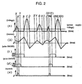
- Fig. 2 is a drawing of waveforms showing time series of changes in
voltage, current, and switch pulse in the same power supply circuit;
- Fig. 3 is a drawing of waveforms showing time series of changes in
voltage, current, and switch pulse in a power supply circuit of a second
exemplary embodiment of this invention;
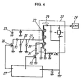
- Fig. 4 is a circuit diagram illustrating a power supply circuit of a
third exemplary embodiment of this invention;
- Fig. 5 is a drawing of waveforms showing time series of changes in
voltage, current, and switch pulse in the same power supply circuit;
- Fig. 6 is a circuit diagram illustrating a power supply circuit of a
fourth exemplary embodiment of this invention;
- Fig. 7 is a drawing of waveforms showing time series of changes in
voltage, current, and switch pulse in the same power supply circuit;
- Fig. 8 is a circuit diagram illustrating a power supply circuit of a
fifth exemplary embodiment of this invention;
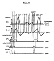
- Fig. 9 is a drawing of waveforms showing time series of changes in
voltage, current, and switch pulse in the same power supply circuit;
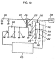
- Fig. 10 is a circuit diagram illustrating a power supply circuit of a
sixth exemplary embodiment of this invention;
- Fig. 11 is a drawing of a waveform showing a high voltage wave
output by a transformer in the same power supply circuit;
- Fig. 12 is another drawing of a waveform showing a high voltage
wave output by a transformer of poor dynamic characteristic;
- Fig. 13 is still another drawing of a waveform showing a high
voltage wave output by a transformer of poor rising characteristic;
- Fig. 14 is a circuit diagram of a power supply circuit of a seventh
exemplary embodiment of this invention;
- Fig.15 is a drawing of waveforms showing time series of changes in
voltage, current, and switch pulse in the same power supply circuit;
- Fig. 16 is a circuit diagram of a power supply circuit of the prior art;
and
- Fig. 17 is a drawing of waveforms showing time series of changes in
voltage, current, and switch pulse in the same power supply circuit.
-
DESCRIPTION OF THE PREFERRED EMBODIMENTS
First Exemplary Embodiment
-
With reference to accompanying figures, a power supply circuit of a
first exemplary embodiment of this invention will be described
herein after.
-
In Fig. 1, the power supply circuit of the first exemplary embodiment
of this invention comprises a driving power supply 23 connected to one
end of terminals of a primary coil 22 of a transformer 21, a first
switching element 24, a capacitor 25 , and a first diode 26, all connected
to the other end of the terminals of the primary coil 22.
-
Furthermore, the first switching element 24 is comprised of a first
MOS type field-effect transistor (MOS FET) that has an internal diode.
This first MOS type field-effect transistor is disposed in a manner that a
drain is connected to the other side terminal of the primary coil 22, a
source is connected to a ground side, and a gate is connected to a PWM
type control circuit 27 , which generates a pulse wave to control the first
switching element 24. It contains the internal diode with an anode
connected to the ground side, and a cathode to the other side terminal of
the primary coil 22. The capacitor 25 has its one end connected to the
other side terminal of the primary coil 22, and the other end connected to
the ground side. The first diode 26 has its cathode connected to the
other side terminal of the primary coil 22, and an anode connected to the
ground side. In addition, the cathode of the first diode 26 and the one
end of the capacitor 25 are connected to a point where the drain of the
first MOS type field-effect transistor and the primary coil 22 make
connection.
-
There is also provided with an auxiliary coil 30, which is mutually
inductive with the primary coil 22, with one of terminals connected to
the ground side. In addition, a second diode 31 and a second switching
element 32 are disposed in connection to the other side of the terminals
of the auxiliary coil 30. The second switching element 32 is comprised
of a second MOS type field-effect transistor having a drain connected to
the other side terminal of the auxiliary coil 30 through the second diode
31, a source connected to the ground side, and a gate connected to the
PWM type control circuit 27. The second diode 31 has an anode.
connected to the other side terminal of the auxiliary coil 30, and a
cathode connected to the drain side of the second MOS type field-effect
transistor. The control circuit 27 is so designed as to switch the second
switching element 32 into an OFF state while the first switching element
24 is in its ON state, and into an ON state when voltage of the primary
coil 22 is greater in value than voltage of the driving power supply after
an electric current flows in the first diode 26 while the first switching
element 24 is in its OFF state.
-
A display 29 (CRT) having high horizontal and vertical scanning
frequency, or the like, is connected to an output side of a secondary coil
28.
-
In this power supply circuit, waveforms of voltage, current and
switch pulses, as they change with a lapse of time, are shown in Fig. 2.
-
In Fig. 2, a reference letter (a) represents a waveform illustrating a
time series of change in value of voltage induced in the primary coil 22
of the transformer 21 taken at a point "O" in the power supply circuit of
Fig. 1; a letter (b) a waveform illustrating a time series of change in
amount of current flowing in the point "O" in the power supply circuit ; a
letter (c) a waveform illustrating a time series of change in shape of an
output wave of the control circuit 27 fed to the first switching element 24,
a letter (d) a waveform illustrating a time series of change in shape of an
output wave of the control circuit 27 fed to the second switching element
32; and a letter (e) a waveform illustrating a time series of change in
amount of current flowing through a point "P" in the power supply
circuit of Fig. 1.
-
During a period of A to B in Fig. 2 , when a pulse wave (the output
wave) of a predetermined duration shown by the waveform (c) is input
from the control circuit 27 to the first switching element 24, making the
first switching element 24 into an ON state, amount of electric current in
the point "O" in Fig. 1 increases with time in proportion to a duration of
the ON state of the first switching element 24 as shown by the waveform
(b), and thereby energy is charged into the primary coil 22.
-
During a period of B to C, when an input of the pulse wave from the
control circuit 27 to the first switching element 24 is ceased as shown by
the waveform (c) , causing the first switching element 24 into an OFF
state, the energy charged in the primary coil 22 begins to be charged into
the capacitor 25, and amount of the current in the point "O" decreases
with time, as shown by the waveform (b). The voltage of the primary
coil 22 reaches its peak value as shown by the waveform (a), when the
charge is completed.
-
During a period of C to D, after completion of the charge into the
capacitor 25 , the energy charged in the capacitor 25 begins to be
recharged into the primary coil 22 again, and amount of the current in the
point "O" decreases with time, as shown by the waveform (b). The
voltage of the primary coil 22 becomes zero as shown by the waveform
(a), when the charge is completed.
-
During a period of D to E, when the charge to the primary coil 22 is
completed, the energy charged in the primary coil 22 is about to start
being recharged into the capacitor 25 again , and this recharge of the
capacitor 25 begins through the ground side due to an effect of a
positive-negative relation in polarity of the voltage across the primary
coil 22. However, a current flows through the first diode 26 having a
low impedance, instead of charging the capacitor 25 , since the first
diode 26 is disposed between the other side terminal of the primary coil
22 and the ground, with the anode connected to the ground side.
Therefore, although amount of the current flowing in the point "O"
increases with time as shown by the waveform (b) , the voltage of the
primary coil 22 remains zero as shown by the waveform (a), since no
energy is charged into the capacitor 25.
-
During a period of E to F, since the energy charged in the primary
coil 22 has been discharged by the flow of current through the first diode
26 , amount of the current shown by the waveform (b) in the point "O"
shall theoretically remain zero, unless the switching element 24 is turned
into an ON state with the waveform (c). In reality, however, amount of
the current through the point "O" increases for a certain period of time as
shown by the waveform (b).
-
A certain amount of energy is therefore charged in the primary coil
22 due to the increase in amount of the current through the point "O".
-
During a period of F to G, the energy charged in the primary coil 22
begins to be charged into the capacitor 25 in the same manner as above,
after the charge to the primary coil 22 is completed. Thus, amount of
the current in the point "O" decreases with time , as shown by the
waveform (b), and the voltage of the primary coil 22 reaches its peak
value as shown by the waveform (a), when the charge is completed.
-
During a period of G to H, after completion of the charge into the
capacitor 25, the energy charged in the capacitor 25 begins to be
recharged into the primary coil 22 again, and amount of the current in the
point "O" decreases with time, as shown by the waveform (b). The
voltage of the primary coil 22 becomes zero as shown by the waveform
(a), when the charge is completed.
-
During a period of H to I, when the charge to the primary coil 22 is
completed, the energy charged in the primary coil 22 is about to start
being recharged into the capacitor 25 again. While amount of the
current in the point "O" increases with time as shown by the waveform
(b) , the voltage of the primary coil 22 remains zero as shown by the
waveform (a), since no energy is charged into the capacitor 25.
-
During a period of I to J, amount of the current in the point "O"
again increases for a certain period of time in the same manner as
described above , as shown by the waveform (b), and energy is hence
charged in the primary coil 22.
-
During a period of J to K (A), after the charge to the primary coil 22
is completed, the energy charged in the primary coil 22 begins to be
charged into the capacitor 25. Amount of the current through the point
"O" decreases with time, as shown by the waveform (b), and the voltage
of the primary coil 22 reaches its peak value as shown by the waveform
(a), when the charge is completed. Since the first switching element 24
is turned into an ON state. during this period, as shown by the waveform
(c), this becomes a new starting point again.
-
In addition, the second switching element 32 is so operated that it
turns into an ON state when voltage of the primary coil 22 is greater than
the voltage level of the driving power supply after an electric current
flows in the first diode 26 while the first switching element 24 is in its
OFF state (at points X and (X)) , and it turns into an OFF state while the
first switching element 24 is in its ON state (at points Y and (Y)).
-
At a time when the second switching element 32 goes into an ON
state as shown by the waveform (d), an electric current flows through the
point "P" simultaneously, as shown by the waveform (e).
-
In a period of (A) through (D), same operations as described above
are repeated.
-
Waveforms of (c) and (d) are adjusted in advance of their timings
according to a cyclic period of the waveform (a).
-
With the above-described composition , voltage of the primary coil
22 decreases to the voltage level of the driving power supply at the
moment the second switching element 32 is turned on, when the voltage
of the primary coil 22 is greater than the voltage of the driving power
supply, and the voltage of the primary coil 22 then becomes zero at the
moment the first switching element 24 is turned into an ON state, since
the second switching element 32 is switched into its ON state when the
voltage of the primary coil 22 is greater than the voltage level of the
driving power supply after electric current flows in the first diode 26
while the first switching element 24 is in its OFF state (at the points X
and (X)).
-
The voltage of the primary coil 22 decreases gradually to the voltage
level of the driving power supply during this moment , because the
energy built up in the transformer 21 is gradually discharged, while the
auxiliary coil 30 is also short-circuited.
-
In other words, there is no sudden change in voltage, and undulation
liable to occur in the current wave can be restricted , since the voltage
always changes from a value equal to or below the voltage of the driving
power supply to zero at the moment the first switching element 24 is
turned on.
-
As described above, the first exemplary embodiment of this
invention eliminates a sudden change in voltage , and restricts the
undulation likely to occur in the current wave, because it always changes
the voltage from a value equal to or below the voltage of the driving
power supply to zero at the moment the first switching element 24 is
turned on.
Second Exemplary Embodiment
-
Referring now to Fig. 1 and Fig. 3, a power supply circuit of a
second exemplary embodiment of this invention will be described
hereinafter.
-
A power supply circuit of the second exemplary embodiment of this
invention employs a change in control function of the control circuit 27
in the power supply circuit, shown in Fig. 1, in the first exemplary
embodiment of this invention.
-
A control circuit 27 of the power supply circuit in the second
exemplary embodiment of this invention generates a pulse wave to
control a first switching element 24 and a second switching element 32 ,
and thereby it switches the second switching element 32 into an OFF
state while the first switching element 24 is in an ON state, and into an
ON state while an electric current is flowing through a first diode 26.
-
In this power supply circuit, waveforms of voltage, current and
switch pulses, as they change with a lapse of time, are shown in Fig. 3.
-
In Fig. 3, a reference letter (a) represents a waveform illustrating a
time series of change in value of voltage induced in a primary coil 22 of
a transformer 21 taken at a point "O" in the power supply circuit ; a
letter (b) a waveform illustrating a time series of change in amount of
current in the point "O" in the power supply circuit; a letter (c) a
waveform illustrating a time series of change in shape of an output wave
of the control circuit 27 fed to the first switching element 24, a letter (d)
a waveform illustrating a time series of change in shape of an output
wave of the control circuit 27 fed to the second switching element 32;
and letter (e) a waveform illustrating a time series of change in amount
of current in a point "P" in the power supply circuit of Fig. 1.
-
During a period of A to C in Fig. 3, when a pulse wave (the output
wave) of a predetermined duration shown by the waveform (c) is input
from the control circuit 27 to the first switching element 24 to turn the
first switching element 24 into an ON state , amount of electric current
through the point "O" increases with time in proportion to a duration of
the ON state of the first switching element 24 as shown by the waveform
(b), and thereby energy is charged into the primary coil 22. An amount
of current in the point "P" remains zero while there is an electric current
flowing in the point "O", since no current flows in the point "P".
-
The pulse wave (output wave) of predetermined duration input to the
second switching element 32 from the control circuit 27 is cut off at any
given timing of a point "B" during the period of A to C, as shown by the
waveform (d), to keep the second switching element 32 in its OFF state.
-
During a period of C to D, when the first switching element 24 is
turned into an OFF state by terminating the input of pulse wave of the
control circuit 27 to the first switching element 24, as shown by the
waveform (c) , the energy charged into the primary coil 22 begins to be
charged into the capacitor 25. This causes the amount of current in the
point "O" to decrease with time as shown by the waveform (b) , and the
voltage of the primary coil 22 reaches its peak value as shown by the
waveform (a), when the charge is completed.
-
During a period of D to E , after completion of the charge into the
capacitor 25, the energy charged in the capacitor 25 begins to be
recharged into the primary coil 22 again, and amount of the current in the
point "O" decreases with time, as shown by the waveform (b). The
voltage of the primary coil 22 becomes zero as shown by the waveform
(a), when the charge is completed.
-
During a period of E to G, when the charge to the primary coil 22 is
completed, the energy charged in the primary coil 22 is about to start
being recharged into the capacitor 25 again , and this recharge of the
capacitor 25 begins through the ground side due to an effect of a
positive-negative relation in polarity of the voltage across the primary
coil 22. However, a current flows through the first diode 26 having a
low impedance , instead of charging the capacitor 25, since there is the
first diode 26 between the other side terminal of the primary coil 22 and
the ground, with the anode connected to the ground side. Therefore,
although amount of the current in the point "O" increases with time as
shown by the waveform (b) , the voltage of the primary coil 22 remains
zero as shown by the waveform (a), since no energy is charged into the
capacitor 25.
-
The pulse wave (output wave) of a predetermined duration from the
control circuit 27 is input to the second switching element 32 at any
given timing of a point "F" during the period of E to G, as shown by the
waveform (d), to keep the second switching element 32 in its ON state.
-
During a period of G to H, since the energy charged in the primary
coil 22 has been discharged by the flow of current through the first diode
26 , amount of the current shown by the waveform (b) in the point "O"
shall theoretically remain zero, unless the switching element 24 is turned
into an ON state with the waveform (c). In reality, however, amount of
the current in the point "O" increases for a certain period of time as
shown by the (b).
-
Although a certain amount of energy is due to be charged in the
primary coil 22 with the increase in amount of the current through the
point "O", no energy is charged in the primary coil 22, because the
second switching element 32 is held in its ON state at the point "F" of
given timing during the period of E to G, which turns the auxiliary coil
30 into a short-circuited condition.
-
This is due generally to the phenomenon involving two coils that are
mutually inductive, in which energy is not charged into one of the coils
even when electric current flows in it, if the other coil is in a short-circuited
condition.
-
During a period of H to I, no energy is charged in the capacitor 25,
since energy is not charged in the primary coil 22. Thus, amount of the
current through the point "O" decreases with time to zero, as shown by
the waveform (b), and the voltage of the primary coil 22 is kept at same
value as the voltage of the driving power supply 23, as shown by the
waveform (a).
-
During a period of I to J(A), when the amount of current becomes
zero as shown by the waveform (b), a current begins to flow in the point
"P" as shown by the waveform (e), to make the voltage of the primary
coil 22 kept at the voltage of the driving power supply, and this
continues until there turns into an ON state in the waveform (c).
-
Subsequently, the same steps are repeated throughout a period of (A)
to (G).
-
With the above-described composition , an electric current, which is
a cause of charging energy in the primary coil 22, flows into the primary
coil 22, after the first switching element 24 turns into its OFF state from
the ON state by the pulse wave generated in the control circuit 27, and
the voltage becomes zero as the current flows for the first time in the
first diode 26. However, the primary coil 22 can be prevented from
being charged with energy, even when the current flows through the
primary coil 22.
-
In an ordinary case, the voltage waveform is liable to be subjected
under an L-C resonance with reference to the voltage of the driving
power supply 23, after the first current flows through the first diode 26.
In the above composition, however, the voltage is maintained constant at
the same voltage as the driving power supply 23, which is greater than
zero.
-
Therefore, this composition can reliably produce the voltage across
the primary coil 22 of the transformer 21 even for a display 29 having
high resolution with high horizontal and vertical scanning frequency , or
the like, since it does not allow electric current to flow through the first
diode 26 at the second time and thereafter, thereby preventing the
phenomenon in that no current flows in the first switching element 24
when the pulse wave is turned into ON state.
-
The control circuit 27, in particular, is so devised that it switches the
second switching element 32 into its ON state while there is an electric
current flowing through the first diode 26. Therefore, the primary coil
22 is not actually charged with energy , even if the electric current, a
cause of charging energy to the primary coil 22, flows in the primary coil
22, after the voltage becomes zero as the current flows through the first
diode 26 for the first time.
-
Accordingly, since no energy is charged in the primary coil 22 to
cause an L-C resonance with reference to the voltage of the driving
power supply 23 , it prevents the resonance from taking place, thereby
maintaining the voltage waveform at the same voltage as the driving
power supply 23 after the first electric current flows through the first
diode 26.
-
According to the second exemplary embodiment, as described above,
the control circuit 27 switches the second switching element 32 into its
ON state while electric current flows through the first diode 26.
Therefor, no energy is actually charged in the primary coil 22, even if the
electric current, a cause of charging energy to the primary coil 22, flows
in the primary coil 22, after the voltage becomes zero due to the first
current flowing through the first diode 26. As the result, it prevents a
resonance from taking place, thereby maintaining the voltage waveform
at the same voltage as the driving power supply 23 after the first electric
current flows through the first diode 26 , since no energy is charged in
the primary coil 22 to cause the L-C resonance with reference to the
voltage of the driving power supply 23.
-
Accordingly, it can prevent the phenomenon in that no current flows
in the first switching element 24 when the first switching element 24 is
switched into its ON state , and produce the voltage reliably across the
primary coil 22 of the transformer, even for the display 29 having high
resolution with high horizontal and vertical scanning frequency, or the
like.
Third Exemplary Embodiment
-
A power supply circuit of a third exemplary embodiment of this
invention will be described hereinafter with reference to the
accompanying figures.
-
In Fig. 4 and Fig. 5, the power supply circuit for a transformer in the
second exemplary embodiment of the present invention is a modified
version of the transformer power supply circuit of the first exemplary
embodiment of this invention. Therefore, the same structural
components are assigned with the same reference numerals.
-
The power supply circuit of the third exemplary embodiment of this
invention has a composition that comprises a third diode 33 provided
between a drain of a MOS type field-effect transistor constituting a first
switching element 24 and a cathode of a first diode 26 , wherein a
cathode of the third diode 33 is connected to a drain of the MOS type
field-effect transistor serving as the first switching element 24, and an
anode of the third diode 33 is connected to the cathode of the first diode
26.
-
In this power supply circuit, waveforms of voltage, current and
switch pulses, as they change with a lapse of time, are shown in Fig. 5.
-
In Fig. 5, a reference letter (a) represents a waveform illustrating a
time series of change in value of voltage induced in a primary coil 22 of
a transformer 21 taken at a point "O" in the power supply circuit ; a
letter (b) a waveform illustrating a time series of change in amount of
current in the point "O" of the power supply circuit; a letter (c) a
waveform illustrating a time series of change in shape of an output wave
of a control circuit 27 fed to the first switching element 24; a letter (d) a
waveform illustrating a time series of change in shape of another output
wave of the control circuit 27 fed to a second switching element 32; and
a letter (e) a waveform illustrating a time series of change in amount of
current at a point "P" of the power supply circuit of Fig. 4. Illustration
of the waveforms in the third exemplary embodiment is identical to the
corresponding illustration in the first exemplary embodiment, except for
the waveforms (a) and (b) in a period between E and K(A).
-
During the period of E through K(A), a voltage shown by the
waveform (a) does not become smaller than zero, even though the
generated voltage indicates an L-C resonance around a driving power
supply voltage, since an addition of the third diode 33 reduces an amount
of current produced, as shown by the waveform (b).
-
Therefore, once an electric current flows through the first diode 26
for the first time, this composition does not allow subsequent current to
flow through it at the second time and thereafter, thereby preventing the
phenomenon that no current flows in the first switching element 24 when
the first switching element 24 is turned into an ON state, as shown by the
waveform (c). Hence, it can produce a voltage reliably across the
primary coil 22 of the transformer, even for a display 29 having high
resolution with high horizontal and vertical scanning frequency, or the
like.
-
Additionally, in the same manner as the power supply circuit of the
first exemplary embodiment , the second switching element 32 is so
operated that it turns into an ON state when voltage of the primary coil
22 is greater than a voltage level of the driving power supply after an
electric current flows in the first diode 26 while the first switching
element 24 is in its OFF state (at points X and (X)), and it turns into an
OFF state while the first switching element 24 is in its ON state (at
points Y and (Y)). Therefore, voltage of the primary coil 22 decreases
to the voltage level of the driving power supply at the moment the
second switching element 32 is turned on , when the voltage of the
primary coil 22 is greater than the voltage of the driving power supply,
and that the voltage of the primary coil 22 becomes zero at the moment
the first switching element 24 is turned on.
-
In other words , there is no sudden change in voltage, and undulation
liable to occur in the current wave can be restricted, since the voltage
always changes from a level equal to or below the voltage of the driving
power supply to zero at the moment the first switching element 24 is
turned on.
-
According to the third exemplary embodiment as described, it can
prevent the phenomenon in that no current flows in the first switching
element 24 , and thereby it can produce a voltage reliably across the
primary coil 22 of the transformer even for the display 29 having high
resolution with high horizontal and vertical scanning frequency, or the
like. In addition , since the voltage always changes from a value equal
to or below the voltage of the driving power supply to zero at the
moment the first switching element 24 is turned on, no sudden change
occurs in voltage, and thereby restricting undulation that is liable to
occur in the current wave.
Fourth Exemplary Embodiment
-
A power supply circuit of a fourth exemplary embodiment of this
invention will be described hereinafter with reference to the
accompanying figures.
-
In Fig. 6, a power supply circuit of the fourth exemplary embodiment
of the present invention is an improved version of the transformer power
supply circuit of the first exemplary embodiment of this invention.
-
The power supply circuit for transformer in this fourth exemplary
embodiment of the invention is provided with a driving power supply
123 connected to one side of terminals of a primary coil 122 of a
transformer 121, a first switching element 124 , a capacitor 125, and a
first diode 126, all connected to the other side of the terminals of the
primary coil 122.
-
Furthermore, the first switching element 124 is comprised of a first
MOS type field-effect transistor (MOS FET) that has an internal diode.
This first MOS type field-effect transistor is disposed in a manner that a
drain is connected to the other side terminal of the primary coil 122 , a
source is connected to a ground side, and a gate is connected to a PWM
type control circuit 127, which generates a pulse wave to control the first
switching element 124. It contains the internal diode with an anode
connected to the ground side, and a cathode to the other side terminal of
the primary coil 122. The capacitor 125 has its one end connected to
the other side terminal of the primary coil 122, and the other end
connected to the ground side. The first diode 126 has its cathode
connected to the other side terminal of the primary coil 122, and an
anode connected to the ground side. The cathode of the first diode 126
and the one end of the capacitor 125 are connected to a point between the
drain of the first MOS type field-effect transistor and the primary coil
122.
-
In addition, there are provided an L-C resonance circuit 135
connected to the primary coil 122, a second diode 131 connected to the
L-C resonance circuit 135, and a second switching element 132
connected to the second diode 131.
-
Moreover, the second switching element 132 is comprised of a
second MOS type field-effect transistor, and this first MOS type field-effect
transistor has a drain connected to a cathode side of the second
diode 131, a source connected to the ground side, and a gate connected to
the control circuit 127. The second diode 131 has its anode connected
to one side of the L-C resonance circuit 135. The L-C resonance circuit
135 has one end connected to the other side terminal of the primary coil
122, and the other end connected to the anode side of the second diode
131.
-
The control circuit 127 generates a pulse wave to control the first
switching element 124 and the second switching element 132 , thereby
the second switching element 132 is switched into an ON state when
voltage of the primary coil 122 is greater than the voltage level of the
driving power supply after an electric current flows in the first diode 126
while the first switching element 124 is in its OFF state (at points X and
(X) in Fig. 7), and into an OFF state while the first switching element
124 is in its ON state (at points Y and (Y) in Fig. 7).
-
In addition, the secondary coil 128 is connected with a display 129
(CRT) having high horizontal and vertical scanning frequency, or the
like.
-
In this power supply circuit, waveforms representing voltage,
current and switch pulses, as they change with a lapse of time, are shown
in Fig. 7.
-
In Fig. 7, a reference letter (a) represents a waveform illustrating a
time series of change in value of voltage induced in the primary coil 122
of the transformer 121 taken at a point "O" in the power supply circuit of
Fig. 6; a letter (b) a waveform illustrating a time series of change in
amount of current flowing in the point "O" in the power supply circuit; a
letter (c) a waveform illustrating a time series of change in shape of an
output wave of a control circuit fed to the first switching element 124; a
letter (d) a waveform illustrating a time series of change in shape of
another output wave of the control circuit fed to the second switching
element 132; and a letter (e) a waveform illustrating a time series of
change in amount of current flowing in a point "P" in the power supply
circuit of Fig. 6.
-
During a period of A to B, when a pulse wave (the output wave) of a
predetermined duration shown by the waveform (c) is input from the
control circuit 127 to the first switching element 124, turning the first
switching element 124 into its ON state, amount of electric current in the
point "O" increases with time in proportion to a duration of the ON state
of the first switching element 124, as shown by the waveform (b), and
thereby energy is charged into the primary coil 122.
-
During a period of B to C, when an input of the pulse wave from the
control circuit 127 to the first switching element 124 is ceased as shown
by the waveform (c), causing the first switching element 124 to turn into
an OFF state, the energy charged in the primary coil 122 begins to be
charged into the capacitor 125, and amount of the current in the point
"O" decreases with time, as shown by the waveform (b). The voltage of
the primary coil 122 reaches its peak value as shown by the waveform (a),
when the charge is completed.
-
During a period of C to D, after completion of the charge into the
capacitor 125, the energy charged in the capacitor 125 begins to be
recharged into the primary coil 122 again, and amount of the current in
the point "O" decreases with time, as shown by the waveform (b). The
voltage of the primary coil 122 becomes zero as shown by the waveform
(a), when the charge is completed.
-
During a period of D to E, when the charge to the primary coil 122 is
completed, the energy charged in the primary coil 122 is about to start
being recharged into the capacitor 125 again, and this recharge of the
capacitor 125 begins through the ground side due to an effect of a
positive-negative relation in polarity of the voltage across the primary
coil 122. However, a current flows through the first diode 126 having a
low impedance, instead of charging the capacitor 125, since the first
diode 126 is disposed between the other side terminal of the primary coil
122 and the ground, with the anode connected to the ground side.
Therefore, although amount of the current in the point "O" increases
with time as shown by the waveform (b) , the voltage of the primary coil
122 remains zero as shown by the waveform (a), since no energy is
charged in the capacitor 125.
-
During a period of E to F, since the energy charged in the primary
coil 122 has been discharged due to a flow of the current through the
first diode 126, amount of the current shown by the waveform (b) in the
point "O" shall theoretically remain zero, unless the switching element
124 is turned into an ON state with the waveform (c). In reality,
however, amount of the current in the point "O" increases for a certain
period of time as shown by the waveform (b).
-
A certain amount of energy is therefore charged in the primary coil
122 due to the increase in amount of the current through the point "O".
-
Subsequently, during a period of F to G, the energy charged in the
primary coil 122 begins to be charged into the capacitor 125 in the same
manner as above, after the charge to the primary coil 122 is completed.
Thus, amount of the current in the point "O" decreases with time , as
shown by the waveform (b), and the voltage of the primary coil 122
reaches its peak value as shown by the waveform (a), when the charge is
completed.
-
During a period of G to H , after completion of the charge into the
capacitor 125, the energy charged in the capacitor 125 begins to be
recharged into the primary coil 122 again, and amount of the current in
the point "O" decreases with time, as shown by the waveform (b). The
voltage of the primary coil 122 becomes zero as shown by the waveform
(a), when the charge is completed.
-
During a period of H to I, when the charge to the primary coil 122 is
completed, the energy charged in the primary coil 122 is about to start
being recharged into the capacitor 125 again. While amount of the
current in the point "O" increases with time as shown by the waveform
(b) , the voltage of the primary coil 122 remains zero as shown by the
waveform (a), since no energy is charged into the capacitor 125.
-
During a period of I to J , amount of the current in the point "O"
again increases for a certain period of time in the same manner as
described above, as shown by the waveform (b), and energy is hence
charged in the primary coil 122.
-
During a period of J to K (A), after the charge to the primary coil
122 is completed, the energy charged in the primary coil 122 begins to be
charged into the capacitor 125. Amount of the current in the point "O"
decreases with time, as shown by the waveform (b), and the voltage of
the primary coil 122 reaches its peak value as shown by the waveform (a),
when the charge is completed. Since the first switching element 124 is
turned into an ON state during this period, as shown by the waveform (c),
this becomes a new starting point again.
-
In addition , the second switching element 132 is so operated that it
turns into an ON state when voltage of the primary coil 122 is greater
than the voltage level of the driving power supply 123 after an electric
current flows in the first diode 126 while the first switching element 124
is in its OFF state (at points X and (X)), and it turns into an OFF state
while the first switching element 124 is in its ON state (at points Y and
(Y)).
-
At a time when the second switching element 132 goes into an ON
state as shown by the waveform (d), an electric current flows through the
point "P" simultaneously , as shown by the waveform (e), and thereby
the voltage output to the primary coil 122 becomes equal to or smaller
than the voltage level of the driving power supply 123, as shown by the
waveform (a), due to an effect of the L-C resonance circuit 135.
-
In this embodiment, the L-C resonance circuit 135 is used as a
waveform shaping circuit for reducing the output voltage to the primary
coil 122 to a value equal to or smaller than the voltage level of the
driving power supply 123 , and it has a resonance time constant in
synchronization with undulation of the current waveform generated in
the primary coil 122, as it outputs a shaping wave that cancels the
undulation of the current generated in the primary coil 122.
-
In respect of the resonance time constant, values of an inductance
(L) and a capacitance (C) employed in the L-C resonance circuit 135 are
determined to satisfy a condition of (a period of fundamental frequency
of the undulation) = 1/ (resonance frequency of the L-C resonance circuit
135).
-
Subsequently, in a period of (A) to (D), same operations as described
above are repeated.
-
With the above-described composition , voltage of the primary coil
122 decreases to nearly zero at the moment the second switching element
132 is turned on, when the voltage of the primary coil 122 is greater than
the voltage of the driving power supply, and the voltage of the primary
coil 122 then becomes zero at the moment the first switching element
124 is turned on, since the second switching element 132 is switched into
its ON state when voltage of the primary coil 122 is greater than the
voltage level of the driving power supply after an electric current flows
in the first diode 126 while the first switching element 124 is in its OFF
state (at the points X and (X)).
-
In other words , there is no sudden change in voltage, and undulation
liable to occur in the current wave can be restricted, since the voltage
always changes from a value equal to or below the voltage of the driving
power supply to zero at the moment the first switching element 124 is
turned on.
-
However, since the first switching element 124 is not turned into its
ON state during a state wherein voltage of the primary coil 122 has
already been zero , there occurs undulation to a certain extent due to this
difference in voltage.
-
This undulation can be suppressed , however, since the L-C
resonance circuit 135 has the resonant time constant in synchronization
with the undulation of the current wave generated in the primary coil 122,
and outputs the shaping wave in a manner to cancel the undulation.
-
According to the fourth exemplary embodiment as described , there
occurs no sudden change in voltage, and undulation liable to occur in the
current wave can be suppressed, since the voltage always changes from a
value equal to or below the voltage of the driving power supply 123 to
zero at the moment the first switching element 124 is turned on.
-
Even if undulation occurs to a certain extent because the voltage of
the primary coil 122 is not zero , although it is equal to or less than the
voltage of the driving power supply 123, at the moment the first
switching element 124 is turned on, the undulation can be suppressed to
a great extent, since the L-C resonance circuit 135 has the resonance
time constant synchronized with the undulation in the current waveform
generated in the primary coil 122, and it outputs the shaping wave that
cancel the undulation.
Fifth Exemplary Embodiment
-
Referring now to the accompanying figures, a power supply circuit
of a fifth exemplary embodiment of this invention will be described
hereinafter.
-
In Fig. 8 and Fig. 9, the power supply circuit for a transformer in the
fifth exemplary embodiment of the present invention is a modified
version of the transformer power supply circuit of the fourth exemplary
embodiment of this invention. Therefore, the same structural
components are assigned with the same reference numerals.
-
The power supply circuit of the fifth exemplary embodiment of this
invention has a composition comprising a third diode 133 disposed
between a drain of a MOS type field-effect transistor constituting a first
switching element 124 and a cathode of a first diode 126 in the
transformer power supply circuit of the fourth exemplary embodiment of
this invention , wherein a cathode of the third diode 133 is connected to
a drain of the MOS type field-effect transistor serving as the first
switching element 124, and an anode of the third diode 133 is connected
to the cathode of the first diode 126.
-
In this power supply circuit, waveforms of voltage, current and
switch pulses, as they change with a lapse of time, are shown in Fig. 9.
-
In Fig. 9 , a reference letter (a) represents a waveform illustrating a
time series of change in value of voltage induced in a primary coil 122 of
a transformer 121 taken at a point "O" in the power supply circuit of Fig.
8; a letter (b) a waveform illustrating a time series of change in amount
of current flowing in the point "O" in the power supply circuit; a letter
(c) a waveform illustrating a time series of change in shape of an output
wave of a control circuit 127 fed to the first switching element 124; a
letter (d) a waveform illustrating a time series of change in shape of an
output wave of the control circuit 127 fed to a second switching element
132; and a letter (e) a waveform illustrating a time series of change in
amount of current flowing in a point "P" in the power supply circuit of
Fig. 8. Illustration of the waveforms in the second exemplary
embodiment is identical to the corresponding illustration in the third
exemplary embodiment, except for the waveforms (a) and (b) in a period
between E and K(A).
-
During the period of E through K(A), a voltage shown by the
waveform (a) does not become smaller than zero, even though the
generated voltage indicates an L-C resonance around a driving power
supply voltage, since an addition of the third diode 133 reduces an
amount of current produced, as shown by the waveform (b).
-
Therefore, once an electric current flows through the first diode 126
for the first time , this composition does not allow subsequent current to
flow through it at the second time and thereafter, thereby preventing the
phenomenon that no current flows in the first switching element 124
when the first switching element 124 is turned into an ON state, as
shown by the waveform (c). Hence, it can produce a voltage reliably
across the primary coil 122 of the transformer 121, even for a display
129 having high resolution with high horizontal and vertical scanning
frequency, or the like.
-
Additionally , in the same manner as the power supply circuit of the
third exemplary embodiment, the second switching element 132 is so
operated that it turns into an ON state when voltage of the primary coil
122 is greater than a voltage level of the driving power supply after an
electric current flows in the first diode 126 while the first switching
element 124 is in its OFF state (at points X and (X) in Fig. 9), and it
turns into an OFF state while the first switching element 124 is in its ON
state (at points Y and (Y) in Fig. 9). Therefore , voltage of the primary
coil 122 decreases to the voltage level of the driving power supply 123 at
the moment the second switching element 132 is turned on, when the
voltage of the primary coil 122 is greater than the voltage of the driving
power supply 123, and that the voltage of the primary coil 122 becomes
zero at the moment the first switching element 124 is turned on.
-
In other words , there occurs no sudden change in voltage, and
undulation liable to occur in the current wave can be restricted, since the
voltage always changes from a level below the voltage of the driving
power supply 123 to zero at the moment the first switching element 124
is turned on.
-
According to the fifth exemplary embodiment as described, it can
prevent the phenomenon that no current flows in the first switching
element 124 , and thereby producing a voltage reliably across the
primary coil 122 of the transformer 121 even for the display 129 having
high resolution with high horizontal and vertical scanning frequency, or
the like, in addition to the advantages attained in the fourth exemplary
embodiment. Moreover, since the voltage always changes from a level
equal to or below the voltage of the driving power supply 123 to zero at
the moment the first switching element 124 is turned on, no sudden
change occurs in the voltage, and thereby restricting undulation that is
liable to occur in the current wave.
-
In the above exemplary embodiment of this invention, although the
L-C resonance circuit 135 has been employed as a waveform shaping
circuit, it may be replaced by a resistance circuit, which outputs such a
shaping wave that absorbs undulation of the current wave generated by
the primary coil 122, to yield a similar effect.
Sixth Exemplary Embodiment
-
Referring now to the accompanying figures, a power supply circuit
of a sixth exemplary embodiment of the present invention will be
described hereinafter.
-
In Fig. 10, the power supply circuit of the sixth exemplary
embodiment of this invention is a modified version of the transformer
power supply circuit of the first exemplary embodiment of this invention
shown in Fig 1.
-
The power supply circuit of the sixth exemplary embodiment of this
invention comprises a flyback transformer represented by a transformer
234 having a primary coil 231 and a secondary coil 232 for supplying
anode voltage to a display 233 such as a display device , a PWM type
control circuit 235 for controlling low output voltage output from the
primary coil 231, and a high-voltage detection circuit 236 for detecting
high output voltage output from the secondary coil 232 as a detected
voltage.
-
The control circuit 235 controls the low output voltage based on the
detected voltage. The high-voltage detection circuit 236 is disposed
between an intermediate point 237 connecting the secondary coil 232 and
the display 233 and the control circuit 235. The high-voltage detection
circuit 236 is so composed that a group of serially connected capacitors
240 comprising a first detection capacitor 238 and a second detection
capacitor 239 and a group of serially connected resistors 243 comprising
a first resistor 241 and a second resistor 242 are connected in parallel
between the intermediate point 237 and a ground , a first midpoint 244
between the first detection capacitor 238 and the second detection
capacitor 239 and a second midpoint 245 between the first resistor 241
and the second resistor 242 are connected with a third detection
capacitor 251, and the second midpoint 245 is connected to the control
circuit 235.
-
Furthermore, the primary coil 231 of the transformer 234 is
connected with a first switching element 246 , a damper diode 247, a
resonance capacitor 248, a diode 249 for canceling a reverse recovery
time of the first switching element 246, and a driving power supply 250.
-
A capacitance (C1) of the first detection capacitor 238 , a
capacitance (C2) of the second detection capacitor 239, a resistance (R1)
of the first resistor 241, and a resistance (R2) of the second resistor 242
are arranged in such values that there is a relation of (C1) × (R1) = (C2) ×
(R2). With a contribution of a capacitance (C3) of the third detection
capacitor 251, the capacitance (C2) of the second detection capacitor 239
may increase or decrease , so as to change the relation of (C1) × (R1) =
(C2) × (R2) to either of (C1) × (R1) > (C2) × (R2) and (C1) × (R1) <(C2)
× (R2).
-
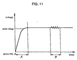
A schematic illustration representing a waveform of the high output
voltage of the transformer 234 is shown in Fig. 11. In this waveform
illustration, a range "A" represents a start-up characteristic of the power
supply circuit at power-on, and a range "B" represents a dynamic
characteristic of the same.
-
Because of the above-described composition , in which the first
midpoint 244 between the first detection capacitor 238 and the second
detection capacitor 239 and the second midpoint 245 between the first
resistor 241 and the second resistor 242 are connected by the third
detection capacitor 251, the capacitance (C2) of the second detection
capacitor 239 comes to be a value derived by adding the capacitance
(C3) of the third detection capacitor 251 to it, at the moment the power
supply circuit is turned on, since all of the first detection capacitor 238,
the second detection capacitor 239, and the third detection capacitor 251
do not carry electric charge, and therefore values of the respective
capacitances (C1), (C2), and (C3) are zero at the moment of power-on.
Hence, their relation with the resistance (R1) of the first resistor 241 and
the resistance (R2) of the second resistor 242 becomes (C1) × (R1) < (C2)
× (R2).
-
Furthermore, since the capacitance (C1) of the first detection
capacitor 238 , the capacitance (C2) of the second detection capacitor
239, and the capacitance (C3) of the third detection capacitor 251 carry
electric charge in a steady state after the power is turned on, a value of
the capacitance (C2) of the second detection capacitor 239 decreases as a
composite capacity, and they become (C1) × (R1) > (C2) × (R2).
-
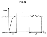
It can therefore improve both of the start-up characteristic and the
dynamic characteristic simultaneously , as shown in Fig. 11, without
holding on to a poor dynamic characteristic as shown in Fig. 12, and a
poor start-up characteristic as shown in Fig. 13.
-
As has been described , since the first midpoint 244 between the first
detection capacitor 238 and the second detection capacitor 239 and the
second midpoint 245 between the first resistor 241 and the second
resistor 242 are connected by the third detection capacitor 251, the sixth
exemplary embodiment can improve the start-up characteristic as well as
the dynamic characteristic at the same time.
Seventh Exemplary Embodiment
-
A power supply circuit of a seventh exemplary embodiment of this
invention will be described hereinafter with reference to the
accompanying figures.
-
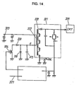
In Fig. 14, a power supply circuit of the seventh exemplary
embodiment of the present invention is an improved version of the
transformer power supply circuit shown in Fig. 1 of the first exemplary
embodiment.
-
The power supply circuit in the seventh exemplary embodiment of
this invention is provided with a driving power supply 323 connected to
one side of terminals of a primary coil 322 of a transformer 321, a first
switching element 324, a capacitor 325, and a first diode 326 , all
connected to the other side of the terminals of the primary coil 322.
-
Furthermore, the first switching element 324 is comprised of a first
MOS type field-effect transistor (MOS FET) that has an internal diode.
This first MOS type field-effect transistor is disposed in a manner that a
drain is connected to the other side terminal of the primary coil 322 , a
source is connected to a ground side, and a gate is connected to a control
circuit 327, which generates a pulse wave to control the first switching
element 324. It contains the internal diode with its anode connected to
the ground side, and a cathode to the other side terminal of the primary
coil 322. The capacitor 325 has its one end connected to the other side
terminal of the primary coil 322, and the other end connected to the
ground side. The first diode 326 has its cathode connected to the other
side terminal of the primary coil 322, and an anode connected to the
ground side. The cathode of the first diode 326 and one end of the
capacitor 325 are connected to a point between the drain of the transistor
and the primary coil.
-
In addition, a third diode 330 is provided between the cathode of the
first diode 326 and the drain of the transistor. The third diode 330 is
disposed with its cathode connected to the drain side of the transistor,
and its anode connected to the cathode side of the first diode 326.
-
Furthermore, one end of the capacitor 325 is connected to a point
between the cathode of the first diode 326 and the primary coil 322.
-
The first diode 326 and the third diode 330 have their current
reverse-recovery time shorter than that of the internal diode of the
transistor. The secondary coil 328 is connected with a display 329
(CRT) having high horizontal and vertical scanning frequency, or the
like.
-
In this power supply circuit, waveforms of voltage, current and
switch pulses, as they change with a lapse of time, are shown in Fig. 15.
-
In Fig. 15, a reference letter (a) represents a waveform illustrating a
time series of change in value of voltage induced in the primary coil 322
of the transformer 321 taken at a point "O" in the power supply circuit of
Fig. 14 ; a letter (b) a waveform illustrating a time series of change in
amount of current in the point "O" of the power supply circuit; and a
letter (c) a waveform illustrating a time series of change in shape of an
output wave of the control circuit 327 fed to the first switching element
324.
-
During a period of A to B, when a pulse wave (the output wave) of a
predetermined duration shown by the waveform (c) is input from the
control circuit 327 to the first switching element 324 , making the first
switching element 324 into an ON state, amount of electric current in the
point "O" increases with time in proportion to a duration of the ON state
of the first switching element 324 as shown by the waveform (b), and
thereby energy is charged into the primary coil 322.
-
During a period of B to C , when an input of the pulse wave from the
control circuit 327 to the first switching element 324 ceases as shown by
the waveform (c), causing the first switching element 324 into an OFF
state, the energy charged in the primary coil 322 begins to be charged
into the capacitor 325, and amount of the current in the point "O"
decreases with time, as shown by the waveform (b). The voltage of the
primary coil 322 reaches its peak value as shown by the waveform (a),
when the charge is completed.
-
During a period of C to D , after a completion of the charge into the
capacitor 325, the energy charged in the capacitor 325 begins to be
recharged into the primary coil 322 again, and amount of the current in
the point "O" decreases with time, as shown by the waveform (b). The
voltage of the primary coil 322 becomes zero as shown by the waveform
(a), when the charge is completed.
-
During a period of D to E , when the charge to the primary coil 322
is completed, the energy charged in the primary coil 322 is about to start
being recharged into the capacitor 325 again, and this recharge of the
capacitor 325 begins through the ground side due to an effect of a
positive-negative relation in polarity of the voltage across the primary
coil 322. However, a current flows through the first diode 326 having a
low impedance, instead of charging the capacitor 325 , since the first
diode 326 is disposed between the other side terminal of the primary coil
322 and the ground, with the anode connected to the ground side.
Therefore, although amount of the current in the point "O" increases
with time as shown by the waveform (b) , the voltage of the primary coil
322 remains zero as shown by the waveform (a), since no energy is
charged in the capacitor 325.
-
During a period of E to F , since the energy charged in the primary
coil 322 has been discharged due to the current flowed through the first
diode 326, amount of the current shown by the waveform (b) in the point
"O" shall theoretically remain zero, unless the switching element 324 is
switched into an ON state with the waveform (c). In reality, however,
amount of the current in the point "O" increases for a certain period of
time as shown by the waveform (b).
-
A certain amount of energy is therefore charged in the primary coil
322 due to the increase in amount of current in the point "O".
-
During a period of F to G, the energy charged into the primary coil
322 begins to be charged into the capacitor 325 in the same manner as
above, after the charge to the primary coil 322 is completed. Thus,
amount of the current in the point "O" decreases with time, as shown by
the waveform (b) , and the voltage of the primary coil 322 reaches its
peak value as shown by the waveform (a), when the charge is completed.
-
During a period of G to H, after completion of the charge into the
capacitor 325, the energy charged in the capacitor 325 begins to be
recharged into the primary coil 322 again, and amount of the current in
the point "O" decreases with time , as shown by the waveform (b). The
voltage of the primary coil 322 becomes equal to the voltage of the
driving power supply 323 as shown by the waveform (a), when the
charge is completed.
-
During a period of H to I, when the charge to the primary coil 322 is
completed , the energy charged in the primary coil 322 begins to be
recharged into the capacitor 325 again, and amount of the current in the
point "O" increases with time, as shown by the waveform (b). The
voltage of the primary coil 322 becomes smaller than the voltage of the
driving power supply 323, but greater than zero, as shown by the
waveform (a), when the charge is completed.
-
During a period of I to J, after completion of the charge into the
capacitor 325, the primary coil 322 begins to be recharged once again.
As amount of the current in the point "O" increases with time, as shown
by the waveform (b) , and the voltage of the primary coil 322 comes to
be equal to the voltage of the driving power supply 323 as shown by the
waveform (a), when the charge is completed.
-
During a period of J to K, after the charge into the primary coil 322
is completed, the energy charged in the primary coil 322 begins to be
charged into the capacitor 325. Amount of the current in the point "O"
decreases with time, as shown by the waveform (b), and the voltage of
the primary coil 322 reaches its peak value as shown by the waveform (a),
when the charge is completed.
-
During a period of K to L, after completion of the charge into the
capacitor 325, the energy charged in the capacitor 325 begins to be
recharged into the primary coil 322. Amount of the current in the point
"O" decreases with time, as shown by the waveform (b) , and the voltage
of the primary coil 322 becomes equal to the voltage of the driving
power supply 323 as shown by the waveform (a), when the charge is
completed.
-
During a period of L to K(A), when the charge to the primary coil
322 is completed, the energy charged in the primary coil 322 begins to be
recharged into the capacitor 325 again, and amount of the current in the
point "O" increases with time, as shown by the waveform (b). While
the voltage of the primary coil 322 becomes smaller than the voltage of
the driving power supply 323 , but greater than zero, as shown by the
waveform (a), upon completion of the charge, the first switching element
324 is turned into its ON state during this period as shown by the
waveform (c). Hence, the same steps as described above are repeated
again at this time, making it a new starting point.
-
The composition , as described above, comprises the third diode 330
disposed between the cathode of the first diode 326 and the drain of the
transistor, i.e. the first switching element 324, with its cathode
connected to the drain side of the transistor and the anode connected to
the cathode side of the first diode 326, and the capacitor 325, of which
one end is connected to a point between the cathode of the first diode
326 and the primary coil 322. In addition, the first diode 326 and the
third diode 330 have their current reverse-recovery time shorter than the
internal diode of the transistor. According to the above composition,
although an electric current , which is a cause of charging energy into the
primary coil 322, flows into the primary coil 322, after the switching
element 324 turns into its OFF state from the ON state with the pulse
wave generated by the control circuit 327, and the voltage becomes zero
as current flows for the first time through the first diode 326, amount of
this electric current can be reduced substantially so as to reduce the
energy charged in the primary coil 322.
-
Accordingly , although an L-C resonance occurs in the voltage
waveform with reference to the voltage of the driving power supply 323,
after the first current flows through the first diode 26, an amplitude of
the resonance can be kept small, and the voltage can be maintained
greater than zero.
-
Therefore, this composition can reliably produce a voltage across the
primary coil 322 of the transformer 321 even for a display 329 having
high resolution with high horizontal and vertical scanning frequency , or
the like, since it does not allow electric current to flow through the first
diode 326 at the second time and thereafter, and to prevent the
phenomenon in that no current flows in the first switching element 324
when the pulse wave is turned into an ON state.
-
In respect of the internal diode , in particular, which is indispensable
for the MOS type field-effect transistor, since the current reverse-recovery
time of the first diode 326 and the third diode 330 is shorter
than that of the internal diode of the transistor, i.e. the first switching
element 324 , a dampening time (the time in which a flow of current
stops, i.e. the current reverse-recovery time) of the current that flows
when the voltage impressed on two ends of the first diode 326 and the
third diode 330 is discharged becomes shorter than that of the internal
diode of the transistor, or, the first switching element 324.
-
As a result, a delaying current (the current that flows after measures
are taken to dampen the current , until the time the current flow actually
stops) due to the first diode 326 and the third diode 330 is suppressed
within a shorter time than a delay current that originates in the internal
diode of the transistor, and thereby the delay current originating in the
internal diode of the transistor is suppressed by the third diode 330 when
the electric current flows from the anode to the cathode of the first diode
326. Moreover, since the delay current that originates in the first diode
326 and the third diode 330 can be suppressed in a shorter time than the
delay current originating in the internal diode of the transistor , it
prevents the transformer and the capacitor from being charged with extra
energy.
-
According to the seventh exemplary embodiment as described , the
third diode 330 is connected between the cathode of the first diode 326
and the drain of the transistor, or the first switching element 324, with
its cathode connected to the drain side of the transistor and the anode
connected to the cathode side of the first diode 326, and one end of the
capacitor 325 is connected to the point between the cathode of the first
diode 326 and the primary coil 322, and further that the first diode 326
and the third diode 330 have their current reverse-recovery time shorter
than the internal diode of the transistor, or the first switching element
324. Therefore, it can positively generate a voltage across the primary
coil 322 of the transformer 321, even for the display 329 that has a high
resolution with high horizontal and vertical scanning frequency, or the
like.
-
In the seventh exemplary embodiment, although one end of the
capacitor 325 is connected to the point between the cathode of the first
diode 326 and the primary coil 322 , the same effect can also be attained
even if it is connected to a point between the cathode of the first diode
326 and the anode of the third diode 330.
INDUSTRIAL APPLICABILITY
-
As described above, the present invention can provide a power
supply circuit that suppresses undulation liable to occur in current wave,
and prevents noise from being generated on an display screen , since it
employs a noise suppression means between a transformer and a control
circuit.
Reference numerals
-
- 21
- transformer
- 22
- primary coil
- 23
- driving power supply
- 24
- first switching element
- 25
- capacitor
- 26
- first diode
- 27
- control circuit
- 28
- secondary coil
- 29
- display
- 30
- Auxiliary coil
- 31
- second diode
- 32
- second switching element
- 33
- third diode
- 121
- transformer
- 122
- primary coil
- 123
- driving power supply
- 124
- first switching element
- 125
- capacitor
- 126
- first diode
- 127
- control circuit
- 128
- secondary coil
- 129
- display
- 130
- Auxiliary coil
- 131
- second diode
- 132
- second switching element
- 133
- third diode
- 135
- L-C resonance circuit
- 231
- primary coil
- 232
- secondary coil
- 233
- display
- 234
- transformer
- 235
- control circuit
- 236
- high voltage detection circuit
- 237
- Intermediate point
- 238
- first detection capacitor
- 239
- second detection capacitor
- 240
- group of capacitors
- 241
- first resistor
- 242
- second resistor
- 243
- group of resistors
- 244
- first middle point
- 245
- second intermediate point
- 246
- first switching element
- 247
- damper diode
- 248
- resonance capacitor
- 249
- diode
- 250
- driving power supply
- 251
- third detection capacitor
- 321
- transformer
- 322
- primary coil
- 323
- driving power supply
- 324
- first switching element
- 325
- capacitor
- 326
- first diode
- 327
- control circuit
- 328
- secondary coil
- 329
- display
- 330
- third diode