EP1065751A2 - Mounting electronic components on circuit boards - Google Patents
Mounting electronic components on circuit boards Download PDFInfo
- Publication number
- EP1065751A2 EP1065751A2 EP00304834A EP00304834A EP1065751A2 EP 1065751 A2 EP1065751 A2 EP 1065751A2 EP 00304834 A EP00304834 A EP 00304834A EP 00304834 A EP00304834 A EP 00304834A EP 1065751 A2 EP1065751 A2 EP 1065751A2
- Authority
- EP
- European Patent Office
- Prior art keywords
- contacts
- board
- component
- connector
- hole
- Prior art date
- Legal status (The legal status is an assumption and is not a legal conclusion. Google has not performed a legal analysis and makes no representation as to the accuracy of the status listed.)
- Granted
Links
- 238000005476 soldering Methods 0.000 claims abstract description 5
- 230000000694 effects Effects 0.000 claims abstract description 3
- 125000006850 spacer group Chemical group 0.000 claims description 5
- 229910000679 solder Inorganic materials 0.000 description 3
- RYGMFSIKBFXOCR-UHFFFAOYSA-N Copper Chemical compound [Cu] RYGMFSIKBFXOCR-UHFFFAOYSA-N 0.000 description 1
- DMFGNRRURHSENX-UHFFFAOYSA-N beryllium copper Chemical compound [Be].[Cu] DMFGNRRURHSENX-UHFFFAOYSA-N 0.000 description 1
- 239000004020 conductor Substances 0.000 description 1
- 229910052802 copper Inorganic materials 0.000 description 1
- 239000010949 copper Substances 0.000 description 1
- 238000000034 method Methods 0.000 description 1
- 230000002093 peripheral effect Effects 0.000 description 1
Images


Classifications
-
- H—ELECTRICITY
- H01—ELECTRIC ELEMENTS
- H01R—ELECTRICALLY-CONDUCTIVE CONNECTIONS; STRUCTURAL ASSOCIATIONS OF A PLURALITY OF MUTUALLY-INSULATED ELECTRICAL CONNECTING ELEMENTS; COUPLING DEVICES; CURRENT COLLECTORS
- H01R12/00—Structural associations of a plurality of mutually-insulated electrical connecting elements, specially adapted for printed circuits, e.g. printed circuit boards [PCB], flat or ribbon cables, or like generally planar structures, e.g. terminal strips, terminal blocks; Coupling devices specially adapted for printed circuits, flat or ribbon cables, or like generally planar structures; Terminals specially adapted for contact with, or insertion into, printed circuits, flat or ribbon cables, or like generally planar structures
- H01R12/70—Coupling devices
- H01R12/71—Coupling devices for rigid printing circuits or like structures
- H01R12/712—Coupling devices for rigid printing circuits or like structures co-operating with the surface of the printed circuit or with a coupling device exclusively provided on the surface of the printed circuit
- H01R12/716—Coupling device provided on the PCB
-
- H—ELECTRICITY
- H01—ELECTRIC ELEMENTS
- H01R—ELECTRICALLY-CONDUCTIVE CONNECTIONS; STRUCTURAL ASSOCIATIONS OF A PLURALITY OF MUTUALLY-INSULATED ELECTRICAL CONNECTING ELEMENTS; COUPLING DEVICES; CURRENT COLLECTORS
- H01R12/00—Structural associations of a plurality of mutually-insulated electrical connecting elements, specially adapted for printed circuits, e.g. printed circuit boards [PCB], flat or ribbon cables, or like generally planar structures, e.g. terminal strips, terminal blocks; Coupling devices specially adapted for printed circuits, flat or ribbon cables, or like generally planar structures; Terminals specially adapted for contact with, or insertion into, printed circuits, flat or ribbon cables, or like generally planar structures
- H01R12/70—Coupling devices
- H01R12/7076—Coupling devices for connection between PCB and component, e.g. display
-
- H—ELECTRICITY
- H01—ELECTRIC ELEMENTS
- H01R—ELECTRICALLY-CONDUCTIVE CONNECTIONS; STRUCTURAL ASSOCIATIONS OF A PLURALITY OF MUTUALLY-INSULATED ELECTRICAL CONNECTING ELEMENTS; COUPLING DEVICES; CURRENT COLLECTORS
- H01R12/00—Structural associations of a plurality of mutually-insulated electrical connecting elements, specially adapted for printed circuits, e.g. printed circuit boards [PCB], flat or ribbon cables, or like generally planar structures, e.g. terminal strips, terminal blocks; Coupling devices specially adapted for printed circuits, flat or ribbon cables, or like generally planar structures; Terminals specially adapted for contact with, or insertion into, printed circuits, flat or ribbon cables, or like generally planar structures
- H01R12/70—Coupling devices
- H01R12/71—Coupling devices for rigid printing circuits or like structures
- H01R12/712—Coupling devices for rigid printing circuits or like structures co-operating with the surface of the printed circuit or with a coupling device exclusively provided on the surface of the printed circuit
- H01R12/716—Coupling device provided on the PCB
- H01R12/718—Contact members provided on the PCB without an insulating housing
-
- H—ELECTRICITY
- H01—ELECTRIC ELEMENTS
- H01R—ELECTRICALLY-CONDUCTIVE CONNECTIONS; STRUCTURAL ASSOCIATIONS OF A PLURALITY OF MUTUALLY-INSULATED ELECTRICAL CONNECTING ELEMENTS; COUPLING DEVICES; CURRENT COLLECTORS
- H01R12/00—Structural associations of a plurality of mutually-insulated electrical connecting elements, specially adapted for printed circuits, e.g. printed circuit boards [PCB], flat or ribbon cables, or like generally planar structures, e.g. terminal strips, terminal blocks; Coupling devices specially adapted for printed circuits, flat or ribbon cables, or like generally planar structures; Terminals specially adapted for contact with, or insertion into, printed circuits, flat or ribbon cables, or like generally planar structures
- H01R12/70—Coupling devices
- H01R12/71—Coupling devices for rigid printing circuits or like structures
- H01R12/72—Coupling devices for rigid printing circuits or like structures coupling with the edge of the rigid printed circuits or like structures
- H01R12/721—Coupling devices for rigid printing circuits or like structures coupling with the edge of the rigid printed circuits or like structures cooperating directly with the edge of the rigid printed circuits
-
- H—ELECTRICITY
- H01—ELECTRIC ELEMENTS
- H01R—ELECTRICALLY-CONDUCTIVE CONNECTIONS; STRUCTURAL ASSOCIATIONS OF A PLURALITY OF MUTUALLY-INSULATED ELECTRICAL CONNECTING ELEMENTS; COUPLING DEVICES; CURRENT COLLECTORS
- H01R29/00—Coupling parts for selective co-operation with a counterpart in different ways to establish different circuits, e.g. for voltage selection, for series-parallel selection, programmable connectors
-
- H—ELECTRICITY
- H05—ELECTRIC TECHNIQUES NOT OTHERWISE PROVIDED FOR
- H05K—PRINTED CIRCUITS; CASINGS OR CONSTRUCTIONAL DETAILS OF ELECTRIC APPARATUS; MANUFACTURE OF ASSEMBLAGES OF ELECTRICAL COMPONENTS
- H05K1/00—Printed circuits
- H05K1/02—Details
- H05K1/14—Structural association of two or more printed circuits
- H05K1/142—Arrangements of planar printed circuit boards in the same plane, e.g. auxiliary printed circuit insert mounted in a main printed circuit
-
- H—ELECTRICITY
- H05—ELECTRIC TECHNIQUES NOT OTHERWISE PROVIDED FOR
- H05K—PRINTED CIRCUITS; CASINGS OR CONSTRUCTIONAL DETAILS OF ELECTRIC APPARATUS; MANUFACTURE OF ASSEMBLAGES OF ELECTRICAL COMPONENTS
- H05K13/00—Apparatus or processes specially adapted for manufacturing or adjusting assemblages of electric components
- H05K13/04—Mounting of components, e.g. of leadless components
Definitions
- This invention relates to mounting electronic components on circuit boards.
- the board has a hole that is large enough to accommodate the body of the component. Connection pads located on the surface of the board near the periphery of the hole are soldered to conductors that lie on the body of the component. Because the component lies partly in the hole, the component does not project above or below the hole as far as it would if it were mounted on the surface of a board that had no hole.
- the finished circuit board assembly, including the components, then may be thinner.
- the invention enables a component to be mounted in any selected position within a range of positions along a direction perpendicular to the board.
- the invention features apparatus for mounting an electronic component on a circuit board.
- the board has a hole that is large enough to accommodate a portion of the component.
- Contacts are arranged along a side wall of the accommodated portion of the component.
- Other contacts are mounted on the board and exposed along the periphery of the hole.
- the contacts on the component (the first contacts) and the contacts on the board (the second contacts) are arranged to effect electrical contact between the first contacts and the second contacts for a range of positions of the component along a direction perpendicular to the board.
- Implementations of the invention may include one or more of the following features.
- a mounting mechanism fixes the component in a selected one of the positions.
- the mounting mechanism includes a portion of the component that is not accommodated by the hole, e.g., a heat sink.
- the mounting mechanism includes spacers.
- the second contacts include compliant pins.
- the first contacts include terminals having surfaces that extend along the direction perpendicular to the board.
- the second contacts are arranged along two opposite edges of the hole and are soldered to the pads on the board.
- the pins are compliant in a direction parallel to a surface of the board.
- the invention features a connector for making electrical connection from a circuit board to first contacts on a component mounted on the board.
- the connector includes second contacts, a connector body supporting the second contacts in a manner that provides mechanically compliant sliding contact between the first contacts and the second contacts when the component is mounted, and a mechanism that enables the connector to be attached to the board by surface mount soldering.
- Implementations of the invention may include one or more of the following features.
- the mechanism includes a solderable clip that engages the connector body and is solderable to a pad on the board.
- the connector has a wall configured to engage a periphery of a hole in the board that accommodates the component.
- the second contacts include prongs that are solderable to pads on the board to connect the component to a circuit on the board.
- the second contacts include pins that are force fitted into holes in the connector body.
- the second contacts include compliant fingers that extend away from the connector body.
- the extent to which the component projects above or below the board can be easily adjusted. This allows different components having different heights to be accommodated on a common version of a circuit board. It also allows units of a given component to be mounted on different boards at different positions to match the different heights of other components mounted on the respective boards.
- the connectors can be mounted using the same surface mount soldering steps that are used to solder other surface mounted components to the board.
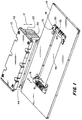
- an electronic component 10 such as a power converter
- a power converter can be mounted at different positions along a direction 12 perpendicular to the plane of a printed circuit board 14 using surface mounted connectors 16, 18.
- the connectors provide mechanical support for the component and electrical connection between conductive pads 31 (figure 2) on the surface of the board, and terminals 20 on the ends 22 of the component.
- each of the connectors includes a plastic body 30, a row of conductive terminations 32 that sit within slots 34 provided in the plastic body, and a pair of mechanical retaining clips 36 that are used to surface mount the connector to the board by soldering the clips to the pads 80.
- the body of the converter has a heat-sinking upper portion 42 that has a larger "footprint" than a lower portion 44 which contains the circuitry of the converter.
- the footprint of the lower portion 44 is roughly matched by a generally rectangular hole 46 in the board 14 so that the lower portion can be accommodated within the hole when the converter is mounted (as seen in figure 6), with appropriate clearance between the periphery of the hole and the outer wall of the converter.
- Opposite ends of the hole 46 extend beyond the footprint of the converter to accommodate the connectors 16, 18 and have cutouts 50 to accommodate the portions 52 of the connectors 16, 18 that enable them to be mounted to the board using clips 36.
- each connector 16 Between the two mounting portions 52 of each connector 16, 18, is a termination support section 60 that includes the slots 34 separated by walls 62.
- the sequence of walls and slots is defined for each connector so that the positions of the terminations 32 match the locations of terminals 20 on the ends of the converter.
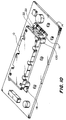
- multiple terminations e.g., a row of closely space terminations 70
- a row of closely space terminations 70 can be provided.
- figure 4 shows a row of closely spaced terminations 70 for use with a wide terminal 21.
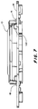
- the connector has a vertical wall 72 with a contour that matches the contour of the peripheral wall of the end of the hole and a horizontal surface 74 that lies against the upper surface of the board.
- Each mounting portion 52 of each connector has a hole 76 to receive a gripping end 78 of one of the mechanical retaining clips.
- the other end of the clip has a flat portion 79 that is soldered to a conductive pad 80 on the surface of the board.
- each of the terminations is stamped from 0.017" thick beryllium-copper sheet and has three "prongs".
- a middle prong 90 has wavy edges that provide a strong friction fit within a vertical hole 92 in the body of the connector.
- a surface mount prong 92 extends horizontally and is soldered to a conductive pad 94 on the surface of the board.
- a third prong 96 serves as a compliant finger (supported at point 98) for contact with a corresponding terminal of the converter.
- Each connector is assembled by insert stitching each of the terminations into one of the slots of the connector.
- the assembled connector is placed into the hole in the board.
- the mechanical retaining clips are mounted on the connector. Using the same surface mount solder process that is used to solder the other surface mounted components, the clips are soldered to their supporting pads and the terminals are soldered to the corresponding conductive pads of the board.
- the terminals 20 on the ends of the converter are formed from 0.012" thick copper sheet and are bent at a ninety-degree angle.
- a vertical portion 102 of each terminal lies within a corresponding slot 104 of a plastic terminal support 106.
- a horizontal portion 108 of each terminal extends along the bottom of the converter and is soldered to a run of a circuit board that extends vertically from inside the main body 110 of the converter in a manner described more completely in United States patent application serial number 08/552,522, filed November 6, 1995.
- a plastic bottom cap 112 covers the horizontal terminal portions.
- a heat sink 114 surrounds the body of the converter and provides the larger footprint portion of the converter.
- the heat sink has four pre-tapped mounting holes 120.
- Four mounting screws 122 (figure 7) extend from the bottom surface of the board, through clearance holes 128 and into the pre-tapped holes to hold the converter securely in place in a way that permits the converter to be removed easily.
- the finger prong 96 makes contact along the surface of the vertical portion of the converter terminal 20.
- the vertical portion of the converter terminal is long enough to permit a good contact to be made at a wide range of vertical positions of the converter.
- the converter In one position, shown in figures 6 and 7, the converter is mounted with the bottom surface of the heat sink in contact with the top surface of the board. The body of the converter then projects more on one side of the board than on the other.
- the bottom of surface of the heat sink is spaced from the board by spacers 130.
- the body of the converter then extends by about equal amounts on opposite sides of the board.
- any needed spacers are put into place and the converter is slipped into the hole in the board.
- the terminals on the converter make contact with, and slide along, the fingers of the terminations until the heat sink reaches its final position with the spacers between the heat sink and the board. The screws are then attached.
- the compliance of the termination fingers enables them to accommodate small variations in the size of the converter body and the configuration of the converter terminals as the converter is being mounted, while still assuring a good electrical connection.
- the component need not be a power converter.
- the hole may have a wide variety of shapes and the number, shape, and locations of the connectors can vary widely.
- the terminations and terminals could be transposed so that the component bears the compliant fingers and the connectors bear the relatively long vertical terminal portions.
Landscapes
- Engineering & Computer Science (AREA)
- Microelectronics & Electronic Packaging (AREA)
- Manufacturing & Machinery (AREA)
- Coupling Device And Connection With Printed Circuit (AREA)
- Multi-Conductor Connections (AREA)
- Structures For Mounting Electric Components On Printed Circuit Boards (AREA)
Abstract
Description
Claims (18)
- Apparatus for mounting an electronic component on a circuit board, comprisinga hole in the board that is large enough to accommodate a portion of the component,first contacts arranged along a side wall of the accommodated portion of the component, andsecond contacts mounted on the board and exposed along the periphery of the hole,the first contacts and the second contacts being arranged to effect electrical contact between the first contacts and the second contacts for a range of positions of the component in a direction perpendicular to the board.
- The apparatus of Claim 1 further comprising a mounting mechanism that fixes the component in a selected one of the positions.
- The apparatus of Claim 2 in which the mounting mechanism includes a portion of the component that is not accommodated by the hole.
- The apparatus of Claim 3 in which the non-accommodated portion comprises a heat sink.
- The apparatus of any of Claims 2 to 4 in which the mounting mechanism includes spacers.
- The apparatus of any preceding claim in which the second contacts comprise compliant pins.
- The apparatus of Claim 6 in which the pins are compliant in a direction parallel to a surface of the board.
- The apparatus of any preceding claim in which the first contacts comprise terminals extending along the perpendicular direction.
- The apparatus of any preceding claim in which the second contacts are arranged along two opposite edges of the hole.
- The apparatus of any preceding claim in which the second contacts are soldered to pads on the board.
- A connector for making electrical connection from a circuit board to first contacts on a component mounted on the board, comprisingsecond contacts,a connector body supporting the second contacts in a manner that provides mechanically compliant sliding contact between the first contacts and the second contacts when the component is mounted, anda mechanism that enables the connector to be attached to the board by surface mount soldering.
- The connector of Claim 11 in which the mechanism comprises a solderable clip that engages the connector body and is solderable to a pad on the board.
- The connector of Claim 11 or Claim 12 in which the connector has a wall configured to engage a periphery of a hole in the board that accommodates the component.
- The connector of any of Claims 11 to 13 in which the second contacts include prongs that are solderable to pads on the board to connect the component to a circuit on the board.
- The connector of any of Claims 11 to 14 in which the second contacts comprise pins that are force fitted into holes in the connector body.
- The connector of any of Claims 11 to 14 in which the second contacts comprise compliant fingers that extend away from the connector body.
- A circuit board assembly comprisinga circuit board with a hole configured to accommodate portion of an electrical component,a connector surface mounted on the circuit board at a periphery of the hole,the connector having second contacts for making electrical contact between a conductive pad on the board and the component,each of the first contacts having a portion that is surface mounted to pads on the circuit board and a portion that is exposed toward the hole in the circuit board to make sliding compliant contact with first contacts on a side wall of the component.
- The combination of a circuit board and an electrical component, which component has first contacts arranged along a side wall portion thereof, the circuit board defining a hole for accommodating a portion of the component, with second contacts mounted on the board and exposed along the periphery of the hole, wherein the hole in the board is adapted to receive the component in a range of positions in a direction perpendicular to the board, in each of which positions there is electrical contact between at least one first contact and at least one second contact.
Applications Claiming Priority (2)
| Application Number | Priority Date | Filing Date | Title |
|---|---|---|---|
| US09/340,707 US6623281B2 (en) | 1999-06-29 | 1999-06-29 | Mounting electronic components on circuit boards |
| US340707 | 1999-06-29 |
Publications (3)
| Publication Number | Publication Date |
|---|---|
| EP1065751A2 true EP1065751A2 (en) | 2001-01-03 |
| EP1065751A3 EP1065751A3 (en) | 2002-01-30 |
| EP1065751B1 EP1065751B1 (en) | 2004-09-08 |
Family
ID=23334596
Family Applications (1)
| Application Number | Title | Priority Date | Filing Date |
|---|---|---|---|
| EP00304834A Expired - Lifetime EP1065751B1 (en) | 1999-06-29 | 2000-06-07 | Mounting electronic components on circuit boards |
Country Status (4)
| Country | Link |
|---|---|
| US (1) | US6623281B2 (en) |
| EP (1) | EP1065751B1 (en) |
| JP (1) | JP2001044594A (en) |
| DE (1) | DE60013505D1 (en) |
Cited By (6)
| Publication number | Priority date | Publication date | Assignee | Title |
|---|---|---|---|---|
| EP1422981A3 (en) * | 2002-11-25 | 2005-09-28 | VLT, Inc. | Packaging and thermal management in electronic apparatus |
| WO2006039655A1 (en) * | 2004-09-30 | 2006-04-13 | Intel Corporation | Apparatus for electrical and optical interconnection |
| US7373031B2 (en) | 2004-09-30 | 2008-05-13 | Intel Corporation | Apparatus for an electro-optical device connection |
| WO2013010608A1 (en) * | 2011-07-19 | 2013-01-24 | Dorma Gmbh + Co. Kg | Door opener with means for detecting positions of movable components of the door opener |
| EP2461227A3 (en) * | 2010-12-03 | 2015-04-01 | ASUSTeK Computer Inc. | Electronic module and electronic device |
| CN105679161A (en) * | 2016-04-01 | 2016-06-15 | 皖西学院 | Nine-jack experimental board capable of being assembled |
Families Citing this family (14)
| Publication number | Priority date | Publication date | Assignee | Title |
|---|---|---|---|---|
| USD510906S1 (en) | 2000-10-27 | 2005-10-25 | Vlt, Inc. | Power converter |
| USD520947S1 (en) | 2001-11-01 | 2006-05-16 | Vlt, Inc. | Power converter body |
| DE10361452A1 (en) * | 2003-12-23 | 2005-10-06 | Demag Cranes & Components Gmbh | Arrangement for attaching electrical and / or electronic components, in particular power components, to a circuit board and housing hereby |
| USD507240S1 (en) | 2004-01-14 | 2005-07-12 | Scientific-Atlanta, Inc | Connector |
| USD507535S1 (en) | 2004-01-14 | 2005-07-19 | Scientific-Atlanta, Inc. | Connector |
| US20050153598A1 (en) * | 2004-01-14 | 2005-07-14 | Meister Douglas L. | Connector assembly |
| US7074054B2 (en) * | 2004-08-06 | 2006-07-11 | Honeywell International Inc. | SMT terminal block |
| US7281930B1 (en) * | 2006-07-27 | 2007-10-16 | Research In Motion Limited | Electrical connector for a printed circuit board |
| US8085541B1 (en) | 2008-04-15 | 2011-12-27 | Vlt, Inc. | Thin flat panel video display |
| US7952879B1 (en) | 2008-04-15 | 2011-05-31 | Vlt, Inc. | System and apparatus for efficient heat removal from heat-generating electronic modules |
| JP5732250B2 (en) * | 2010-12-28 | 2015-06-10 | 日本航空電子工業株式会社 | Connector unit and connector device |
| CN107454791B (en) * | 2017-07-25 | 2020-05-08 | 浙江云时代智能制造有限公司 | Wall panel combination connected with movable circuit board of electric connector |
| EP3764758A1 (en) * | 2019-07-12 | 2021-01-13 | Verisure Sàrl | Printed circuit board with soldered conductive element |
| JP7417842B2 (en) * | 2020-09-09 | 2024-01-19 | 株式会社オートネットワーク技術研究所 | surface mount connector |
Family Cites Families (15)
| Publication number | Priority date | Publication date | Assignee | Title |
|---|---|---|---|---|
| US4417296A (en) * | 1979-07-23 | 1983-11-22 | Rca Corp | Method of connecting surface mounted packages to a circuit board and the resulting connector |
| JPS6010297Y2 (en) * | 1981-11-24 | 1985-04-09 | ソニー株式会社 | connector |
| JPS6013413A (en) * | 1983-07-05 | 1985-01-23 | 住友電気工業株式会社 | Device for mutually connecting wire ring harness |
| US4603927A (en) * | 1984-07-12 | 1986-08-05 | Rogers Corporation | Surface mounted bussing device |
| US4603929A (en) * | 1985-02-13 | 1986-08-05 | Northern Telecom Limited | Connector shroud |
| DE3720925A1 (en) | 1987-06-25 | 1989-01-05 | Wabco Westinghouse Fahrzeug | PCB |
| JPH02215068A (en) | 1989-02-15 | 1990-08-28 | Nippon Kaiheiki Kogyo Kk | Control apparatus for printed board |
| JPH03163893A (en) * | 1989-11-21 | 1991-07-15 | Fujitsu Ltd | Footprint board for mounting smd additionally |
| JPH0433278A (en) * | 1990-05-29 | 1992-02-04 | Fujikura Ltd | Connector |
| US5249971A (en) | 1991-09-13 | 1993-10-05 | Foxconn International, Inc. | IC package connector |
| JP3163893B2 (en) | 1994-03-15 | 2001-05-08 | 東急車輛製造株式会社 | Guidance method for waste transport vehicles |
| US5605464A (en) | 1994-03-22 | 1997-02-25 | Molex Incorporated | IC package connector |
| US5675888A (en) | 1994-07-25 | 1997-10-14 | Owen; Marvin Leroy | Molded printed circuit board with wipe-in connector and method of making same |
| US6031726A (en) | 1995-11-06 | 2000-02-29 | Vlt Corporation | Low profile mounting of power converters with the converter body in an aperture |
| US6000125A (en) * | 1996-01-30 | 1999-12-14 | Samsung Electronics America, Inc. | Method of heat dissipation from two surfaces of a microprocessor |
-
1999
- 1999-06-29 US US09/340,707 patent/US6623281B2/en not_active Expired - Lifetime
-
2000
- 2000-06-07 EP EP00304834A patent/EP1065751B1/en not_active Expired - Lifetime
- 2000-06-07 DE DE60013505T patent/DE60013505D1/en not_active Expired - Lifetime
- 2000-06-29 JP JP2000196315A patent/JP2001044594A/en active Pending
Cited By (12)
| Publication number | Priority date | Publication date | Assignee | Title |
|---|---|---|---|---|
| EP1422981A3 (en) * | 2002-11-25 | 2005-09-28 | VLT, Inc. | Packaging and thermal management in electronic apparatus |
| US7799615B2 (en) | 2002-11-25 | 2010-09-21 | Vlt, Inc. | Power converter package and thermal management |
| WO2006039655A1 (en) * | 2004-09-30 | 2006-04-13 | Intel Corporation | Apparatus for electrical and optical interconnection |
| US7373031B2 (en) | 2004-09-30 | 2008-05-13 | Intel Corporation | Apparatus for an electro-optical device connection |
| US7660128B2 (en) | 2004-09-30 | 2010-02-09 | Emcore Corporation | Apparatus for electrical and optical interconnection |
| US7661886B2 (en) | 2004-09-30 | 2010-02-16 | Emcore Corporation | Apparatus for electro-optical device connection |
| EP2461227A3 (en) * | 2010-12-03 | 2015-04-01 | ASUSTeK Computer Inc. | Electronic module and electronic device |
| WO2013010608A1 (en) * | 2011-07-19 | 2013-01-24 | Dorma Gmbh + Co. Kg | Door opener with means for detecting positions of movable components of the door opener |
| CN103688006A (en) * | 2011-07-19 | 2014-03-26 | 多玛两合有限公司 | Door opener with means for detecting positions of movable components of the door opener |
| CN103688006B (en) * | 2011-07-19 | 2016-09-14 | 多玛德国有限公司 | There is the door opener of the device of the position of movable-component for detecting door opener |
| CN105679161A (en) * | 2016-04-01 | 2016-06-15 | 皖西学院 | Nine-jack experimental board capable of being assembled |
| CN105679161B (en) * | 2016-04-01 | 2018-08-28 | 皖西学院 | A kind of nine hole experimental plate of sectional |
Also Published As
| Publication number | Publication date |
|---|---|
| EP1065751A3 (en) | 2002-01-30 |
| JP2001044594A (en) | 2001-02-16 |
| US20020016094A1 (en) | 2002-02-07 |
| DE60013505D1 (en) | 2004-10-14 |
| US6623281B2 (en) | 2003-09-23 |
| EP1065751B1 (en) | 2004-09-08 |
Similar Documents
| Publication | Publication Date | Title |
|---|---|---|
| EP1065751B1 (en) | Mounting electronic components on circuit boards | |
| US3873173A (en) | Electrical connector assembly | |
| JP4883655B2 (en) | Electrical connector with electrical shield having latch and mounting arm | |
| US4225209A (en) | Electrical connector receptacle | |
| EP1280240B1 (en) | A socketable flexible circuit based electronic device module and a socket for the same | |
| US6080008A (en) | Push-wire contact | |
| JPS61292395A (en) | Electric circuit board assembly | |
| US3710299A (en) | Low profile socket for integrated circuit pack | |
| EP0709931A2 (en) | Surface mountable board edge connector | |
| US7097466B2 (en) | Electronic part-mounting socket | |
| JPH07326450A (en) | Socket and manufacturing method thereof | |
| US4629267A (en) | Circuit terminating device | |
| EP0766854B1 (en) | Sim card connector | |
| JP2003168533A (en) | Electric connector terminal | |
| EP0109297A1 (en) | Improvements in electrical contact members and electrical connector assemblies | |
| US7883344B1 (en) | Electrical connector | |
| JP4035846B2 (en) | Shield structure and method of forming the same | |
| JP2967480B2 (en) | Electrical connector | |
| JP2003187932A (en) | Electric socket | |
| JP4454137B2 (en) | PCB mounting spring | |
| US5564932A (en) | Customizeable interconnect device for stacking electrical components of varying configuration | |
| US4580857A (en) | Circuit terminating clip | |
| JP3016058B2 (en) | Electrical connector for card | |
| EP0997982A2 (en) | Electrical connector for printed circuit boards | |
| JP3569847B2 (en) | Card connector |
Legal Events
| Date | Code | Title | Description |
|---|---|---|---|
| PUAI | Public reference made under article 153(3) epc to a published international application that has entered the european phase |
Free format text: ORIGINAL CODE: 0009012 |
|
| 17P | Request for examination filed |
Effective date: 20000614 |
|
| AK | Designated contracting states |
Kind code of ref document: A2 Designated state(s): AT BE CH CY DE DK ES FI FR GB GR IE IT LI LU MC NL PT SE Kind code of ref document: A2 Designated state(s): DE FR GB |
|
| AX | Request for extension of the european patent |
Free format text: AL;LT;LV;MK;RO;SI |
|
| RIC1 | Information provided on ipc code assigned before grant |
Free format text: 7H 01R 12/16 A, 7H 05K 1/18 B, 7H 01R 29/00 B |
|
| PUAL | Search report despatched |
Free format text: ORIGINAL CODE: 0009013 |
|
| AK | Designated contracting states |
Kind code of ref document: A3 Designated state(s): AT BE CH CY DE DK ES FI FR GB GR IE IT LI LU MC NL PT SE |
|
| AX | Request for extension of the european patent |
Free format text: AL;LT;LV;MK;RO;SI |
|
| AKX | Designation fees paid |
Free format text: DE FR GB |
|
| 17Q | First examination report despatched |
Effective date: 20021118 |
|
| GRAP | Despatch of communication of intention to grant a patent |
Free format text: ORIGINAL CODE: EPIDOSNIGR1 |
|
| GRAP | Despatch of communication of intention to grant a patent |
Free format text: ORIGINAL CODE: EPIDOSNIGR1 |
|
| GRAS | Grant fee paid |
Free format text: ORIGINAL CODE: EPIDOSNIGR3 |
|
| GRAS | Grant fee paid |
Free format text: ORIGINAL CODE: EPIDOSNIGR3 |
|
| GRAS | Grant fee paid |
Free format text: ORIGINAL CODE: EPIDOSNIGR3 |
|
| GRAA | (expected) grant |
Free format text: ORIGINAL CODE: 0009210 |
|
| AK | Designated contracting states |
Kind code of ref document: B1 Designated state(s): DE FR GB |
|
| PG25 | Lapsed in a contracting state [announced via postgrant information from national office to epo] |
Ref country code: FR Free format text: LAPSE BECAUSE OF NON-PAYMENT OF DUE FEES Effective date: 20040908 |
|
| REG | Reference to a national code |
Ref country code: GB Ref legal event code: FG4D |
|
| REG | Reference to a national code |
Ref country code: IE Ref legal event code: FG4D |
|
| REF | Corresponds to: |
Ref document number: 60013505 Country of ref document: DE Date of ref document: 20041014 Kind code of ref document: P |
|
| PG25 | Lapsed in a contracting state [announced via postgrant information from national office to epo] |
Ref country code: DE Free format text: LAPSE BECAUSE OF FAILURE TO SUBMIT A TRANSLATION OF THE DESCRIPTION OR TO PAY THE FEE WITHIN THE PRESCRIBED TIME-LIMIT Effective date: 20041209 |
|
| PGFP | Annual fee paid to national office [announced via postgrant information from national office to epo] |
Ref country code: GB Payment date: 20050602 Year of fee payment: 6 |
|
| PLBE | No opposition filed within time limit |
Free format text: ORIGINAL CODE: 0009261 |
|
| STAA | Information on the status of an ep patent application or granted ep patent |
Free format text: STATUS: NO OPPOSITION FILED WITHIN TIME LIMIT |
|
| 26N | No opposition filed |
Effective date: 20050609 |
|
| EN | Fr: translation not filed | ||
| PG25 | Lapsed in a contracting state [announced via postgrant information from national office to epo] |
Ref country code: GB Free format text: LAPSE BECAUSE OF NON-PAYMENT OF DUE FEES Effective date: 20060607 |
|
| GBPC | Gb: european patent ceased through non-payment of renewal fee |
Effective date: 20060607 |