EP1065713A2 - Staged aluminium deposition process for filling vias - Google Patents
Staged aluminium deposition process for filling vias Download PDFInfo
- Publication number
- EP1065713A2 EP1065713A2 EP00113013A EP00113013A EP1065713A2 EP 1065713 A2 EP1065713 A2 EP 1065713A2 EP 00113013 A EP00113013 A EP 00113013A EP 00113013 A EP00113013 A EP 00113013A EP 1065713 A2 EP1065713 A2 EP 1065713A2
- Authority
- EP
- European Patent Office
- Prior art keywords
- pvd
- layer
- metal
- substrate
- metal layer
- Prior art date
- Legal status (The legal status is an assumption and is not a legal conclusion. Google has not performed a legal analysis and makes no representation as to the accuracy of the status listed.)
- Withdrawn
Links
Images


Classifications
-
- H—ELECTRICITY
- H10—SEMICONDUCTOR DEVICES; ELECTRIC SOLID-STATE DEVICES NOT OTHERWISE PROVIDED FOR
- H10W—GENERIC PACKAGES, INTERCONNECTIONS, CONNECTORS OR OTHER CONSTRUCTIONAL DETAILS OF DEVICES COVERED BY CLASS H10
- H10W20/00—Interconnections in chips, wafers or substrates
- H10W20/01—Manufacture or treatment
- H10W20/031—Manufacture or treatment of conductive parts of the interconnections
- H10W20/056—Manufacture or treatment of conductive parts of the interconnections by filling conductive material into holes, grooves or trenches
- H10W20/059—Manufacture or treatment of conductive parts of the interconnections by filling conductive material into holes, grooves or trenches by reflowing or applying pressure
-
- C—CHEMISTRY; METALLURGY
- C23—COATING METALLIC MATERIAL; COATING MATERIAL WITH METALLIC MATERIAL; CHEMICAL SURFACE TREATMENT; DIFFUSION TREATMENT OF METALLIC MATERIAL; COATING BY VACUUM EVAPORATION, BY SPUTTERING, BY ION IMPLANTATION OR BY CHEMICAL VAPOUR DEPOSITION, IN GENERAL; INHIBITING CORROSION OF METALLIC MATERIAL OR INCRUSTATION IN GENERAL
- C23C—COATING METALLIC MATERIAL; COATING MATERIAL WITH METALLIC MATERIAL; SURFACE TREATMENT OF METALLIC MATERIAL BY DIFFUSION INTO THE SURFACE, BY CHEMICAL CONVERSION OR SUBSTITUTION; COATING BY VACUUM EVAPORATION, BY SPUTTERING, BY ION IMPLANTATION OR BY CHEMICAL VAPOUR DEPOSITION, IN GENERAL
- C23C14/00—Coating by vacuum evaporation, by sputtering or by ion implantation of the coating forming material
- C23C14/06—Coating by vacuum evaporation, by sputtering or by ion implantation of the coating forming material characterised by the coating material
- C23C14/14—Metallic material, boron or silicon
- C23C14/18—Metallic material, boron or silicon on other inorganic substrates
-
- H—ELECTRICITY
- H10—SEMICONDUCTOR DEVICES; ELECTRIC SOLID-STATE DEVICES NOT OTHERWISE PROVIDED FOR
- H10P—GENERIC PROCESSES OR APPARATUS FOR THE MANUFACTURE OR TREATMENT OF DEVICES COVERED BY CLASS H10
- H10P14/00—Formation of materials, e.g. in the shape of layers or pillars
- H10P14/40—Formation of materials, e.g. in the shape of layers or pillars of conductive or resistive materials
- H10P14/42—Formation of materials, e.g. in the shape of layers or pillars of conductive or resistive materials using a gas or vapour
- H10P14/44—Physical vapour deposition [PVD]
-
- H—ELECTRICITY
- H10—SEMICONDUCTOR DEVICES; ELECTRIC SOLID-STATE DEVICES NOT OTHERWISE PROVIDED FOR
- H10W—GENERIC PACKAGES, INTERCONNECTIONS, CONNECTORS OR OTHER CONSTRUCTIONAL DETAILS OF DEVICES COVERED BY CLASS H10
- H10W20/00—Interconnections in chips, wafers or substrates
- H10W20/01—Manufacture or treatment
- H10W20/031—Manufacture or treatment of conductive parts of the interconnections
- H10W20/032—Manufacture or treatment of conductive parts of the interconnections of conductive barrier, adhesion or liner layers
- H10W20/033—Manufacture or treatment of conductive parts of the interconnections of conductive barrier, adhesion or liner layers in openings in dielectrics
- H10W20/035—Manufacture or treatment of conductive parts of the interconnections of conductive barrier, adhesion or liner layers in openings in dielectrics combinations of barrier, adhesion or liner layers, e.g. multi-layered barrier layers
-
- C—CHEMISTRY; METALLURGY
- C23—COATING METALLIC MATERIAL; COATING MATERIAL WITH METALLIC MATERIAL; CHEMICAL SURFACE TREATMENT; DIFFUSION TREATMENT OF METALLIC MATERIAL; COATING BY VACUUM EVAPORATION, BY SPUTTERING, BY ION IMPLANTATION OR BY CHEMICAL VAPOUR DEPOSITION, IN GENERAL; INHIBITING CORROSION OF METALLIC MATERIAL OR INCRUSTATION IN GENERAL
- C23C—COATING METALLIC MATERIAL; COATING MATERIAL WITH METALLIC MATERIAL; SURFACE TREATMENT OF METALLIC MATERIAL BY DIFFUSION INTO THE SURFACE, BY CHEMICAL CONVERSION OR SUBSTITUTION; COATING BY VACUUM EVAPORATION, BY SPUTTERING, BY ION IMPLANTATION OR BY CHEMICAL VAPOUR DEPOSITION, IN GENERAL
- C23C14/00—Coating by vacuum evaporation, by sputtering or by ion implantation of the coating forming material
- C23C14/22—Coating by vacuum evaporation, by sputtering or by ion implantation of the coating forming material characterised by the process of coating
- C23C14/34—Sputtering
- C23C14/3407—Cathode assembly for sputtering apparatus, e.g. Target
-
- C—CHEMISTRY; METALLURGY
- C23—COATING METALLIC MATERIAL; COATING MATERIAL WITH METALLIC MATERIAL; CHEMICAL SURFACE TREATMENT; DIFFUSION TREATMENT OF METALLIC MATERIAL; COATING BY VACUUM EVAPORATION, BY SPUTTERING, BY ION IMPLANTATION OR BY CHEMICAL VAPOUR DEPOSITION, IN GENERAL; INHIBITING CORROSION OF METALLIC MATERIAL OR INCRUSTATION IN GENERAL
- C23C—COATING METALLIC MATERIAL; COATING MATERIAL WITH METALLIC MATERIAL; SURFACE TREATMENT OF METALLIC MATERIAL BY DIFFUSION INTO THE SURFACE, BY CHEMICAL CONVERSION OR SUBSTITUTION; COATING BY VACUUM EVAPORATION, BY SPUTTERING, BY ION IMPLANTATION OR BY CHEMICAL VAPOUR DEPOSITION, IN GENERAL
- C23C14/00—Coating by vacuum evaporation, by sputtering or by ion implantation of the coating forming material
- C23C14/22—Coating by vacuum evaporation, by sputtering or by ion implantation of the coating forming material characterised by the process of coating
- C23C14/56—Apparatus specially adapted for continuous coating; Arrangements for maintaining the vacuum, e.g. vacuum locks
Definitions
- the metallization process is carried out in an integrated processing system that includes PVD chambers for depositing a metal such as aluminum without the formation of an oxide layer over the aluminum layers.
- the processing system may also contain reflow chambers, preclean chambers, and barrier layer chambers associated with deposition of the metal layers.
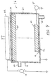
- the via 14 is filled with Al by reflowing a bulk PVD Al layer 23 deposited on the conformal PVD Al layer (layer 22 of Figure 1).
- An integrated PVD Al layer 24 will result from integrating the bulk PVD Al layer 23 that is deposited onto the conformal PVD Al layer 22.
- the bulk PVD Al may contain certain dopants, and upon deposition the bulk PVD Al layer 23 may integrate with the conformal PVD Al layer 22 so that the dopant is dispersed throughout much of the integrated PVD Al layer 24. In general, the integrated PVD Al layer 24 does not need to be doped.
- the top surface 26 of the integrated PVD Al layer 24 is substantially planarized. Because the titanium layer 16 provides good wetting of the conformal PVD Al layer 22, the dielectric layer or substrate temperature during deposition of PVD Al may be from about room temperature to about 500°C.
- the particular embodiment of the apparatus 35 shown herein is suitable for processing planar substrates, such as semiconductor substrates, and is provided to illustrate the invention, and should not be used to limit the scope of the invention.
- the apparatus 35 typically comprises a cluster of interconnected process chambers including at least one long throw PVD metal chamber.
- the apparatus 35 preferably includes a PVD Al chamber 36 having a substrate to target spacing of at least 100 mm for depositing conformal PVD Al layers, and two additional PVD Al chambers 38 for depositing and reflowing PVD Al layers.
- a sputtering target 64 and a semiconductor substrate 66 are contained within a grounded enclosure wall 60, which may be a chamber wall as shown or a grounded shield.
- the target 64 and the substrate are separated by a long throw distance of at least about 100 mm, preferably from about 150 mm to about 190 mm.
- the long throw chamber may also contain a collimator (not shown) between the target 64 and the substrate 66 if needed to provide a more uniform and symmetrical flux of deposition material to each location on the substrate 66.
- Collimators that may be used in the PVD chamber are described in United States Patent Application No, 08/792,292, filed January 31, 1997, which description is incorporated by reference herein.
- a process gas comprising a non-reactive species such as Ar, is charged into the PVD chamber 36 through the gas inlet 68 at a selected flow rate regulated by a mass flow controller (not shown).
- the chamber pressure is controlled by varying the rate that process gases are pumped through the exhaust outlet 70 and is maintained below about 1 milliTorr to promote deposition of conformal PVD metal layers, preferably from about 0.2 milliTorr to about 0.5 milliTorr.
- the chamber manager subroutine 144A selectively schedules or calls the process component subroutines in accordance within the particular process set being executed.
- the chamber manager subroutine 144A schedules the process component subroutines similarly to how the sequencer subroutine 143 schedules which process chamber 36 and process set is to be executed next.
- the chamber manager subroutine 144A includes steps of monitoring the various chamber components, determining which components needs to be operated based on the process parameters for the process set to be executed, and causing execution of a chamber component subroutine responsive to the monitoring and determining steps.
Landscapes
- Chemical & Material Sciences (AREA)
- Inorganic Chemistry (AREA)
- Chemical Kinetics & Catalysis (AREA)
- Engineering & Computer Science (AREA)
- Materials Engineering (AREA)
- Mechanical Engineering (AREA)
- Metallurgy (AREA)
- Organic Chemistry (AREA)
- Electrodes Of Semiconductors (AREA)
- Internal Circuitry In Semiconductor Integrated Circuit Devices (AREA)
- Physical Vapour Deposition (AREA)
Abstract
Description
Claims (20)
- A method of forming a feature on a substrate, comprising:a) depositing a barrier/wetting layer over the surfaces of an aperture in the substrate, the barrier/wetting layer having a thickness of between about 5 and about 700 Angstroms;b) physical vapor depositing a conformal metal layer over the surface of the barrier/wetting layer without capping or filling the aperture at a chamber pressure less than about 1 milliTorr, the physical vapor deposited metal layer having a thickness between about 200 Angstroms and about 1 micron; andc) filling the aperture with metal.
- The method of claim 1, wherein filling the aperture with metal comprises reflowing a second deposited metal layer into the aperture.
- The method of claim 1, wherein filling the aperture with metal comprises physical vapor depositing a bulk PVD metal layer on the conformal PVD metal layer and reflowing the bulk metal layer.
- The method of claim 1, wherein a) through c) are performed sequentially in an integrated processing system with a common vacuum mainframe.
- The method of claim 1, wherein a) through c) are performed in separate chambers.
- The method of claim 1, wherein the metal is not exposed to air prior to filling the aperture.
- The method of claim 1, wherein the metal is sputtered from a target located from about 150 mm to about 190 mm from the substrate.
- The method of claim 1, wherein the metal layer is an aluminum layer.
- A process for filling a via, trench, or dual damascene structure on a substrate, comprising:a) depositing a conformal barrier/wetting layer on the substrate;b) depositing a conformal PVD metal layer over the barrier/wetting layer at a chamber pressure less than about 1 milliTorr; andc) reflowing a bulk PVD metal layer deposited on the conformal PVD metal layer.
- The process of claim 9, wherein the conformal PVD metal layer has a blanket thickness from about 200 Angstroms to about 1micron.
- The process of claim 10, wherein the barrier/wetting layer has a thickness from about 5 Angstroms to about 700 Angstroms.
- The process of claim 9, wherein the barrier/wetting layer is titanium.
- The process of claim 9 wherein the barrier/wetting layer is selected from a group consisting of tungsten (W), niobium (Nb), aluminum silicates, tantalum (Ta), tantalum nitride (TaN), titanium nitride (TiN), PVD Ti/N2-stuffed, TiSiN, WSiN, or a combination thereof.
- The process of claim 9, wherein the conformal PVD metal layer is a conformal PVD aluminum layer.
- The process of claim 9, wherein the bulk PVD metal layer is maintained at a temperature less than 500°C while reflowing the bulk metal layer.
- The process of claim 9, wherein the conformal PVD metal layer is sputtered from a target located from about 150 mm to about 190 mm from the substrate.
- The process of claim 16, wherein the conformal PVD metal layer is sputtered at a chamber pressure less than about 0.35 milliTorr.
- An apparatus for depositing metal layers, comprising:a substrate transfer chamber;a barrier/wetting layer chamber connected to the transfer chamber;a long throw physical vapor deposition chamber connected to the transfer chamber, the physical vapor deposition chamber comprising a target and a substrate separated by a long throw distance of at least 100 mm; anda hot metal physical vapor deposition chamber connected to the transfer chamber.
- The apparatus of claim 18, wherein the long throw distance is from about 150 mm to about 190 mm.
- The apparatus of claim 19, wherein the hot metal physical vapor deposition chamber is also a metal reflow chamber.
Applications Claiming Priority (2)
| Application Number | Priority Date | Filing Date | Title |
|---|---|---|---|
| US340977 | 1999-06-28 | ||
| US09/340,977 US6352620B2 (en) | 1999-06-28 | 1999-06-28 | Staged aluminum deposition process for filling vias |
Publications (2)
| Publication Number | Publication Date |
|---|---|
| EP1065713A2 true EP1065713A2 (en) | 2001-01-03 |
| EP1065713A3 EP1065713A3 (en) | 2001-05-23 |
Family
ID=23335731
Family Applications (1)
| Application Number | Title | Priority Date | Filing Date |
|---|---|---|---|
| EP00113013A Withdrawn EP1065713A3 (en) | 1999-06-28 | 2000-06-21 | Staged aluminium deposition process for filling vias |
Country Status (5)
| Country | Link |
|---|---|
| US (2) | US6352620B2 (en) |
| EP (1) | EP1065713A3 (en) |
| JP (1) | JP2001044204A (en) |
| KR (1) | KR20010007557A (en) |
| TW (1) | TW451410B (en) |
Cited By (2)
| Publication number | Priority date | Publication date | Assignee | Title |
|---|---|---|---|---|
| WO2020139436A1 (en) * | 2018-12-27 | 2020-07-02 | Raytheon Company | Method of filling grooves and holes in a substrate |
| CN121076048A (en) * | 2025-10-30 | 2025-12-05 | 杭州富芯半导体有限公司 | Semiconductor chip, preparation method of metal interconnection layer and metal interconnection layer |
Families Citing this family (34)
| Publication number | Priority date | Publication date | Assignee | Title |
|---|---|---|---|---|
| US6352620B2 (en) * | 1999-06-28 | 2002-03-05 | Applied Materials, Inc. | Staged aluminum deposition process for filling vias |
| KR100434188B1 (en) * | 2001-08-28 | 2004-06-04 | 삼성전자주식회사 | Method for depositing barrier metal layer |
| US7220098B2 (en) | 2003-05-27 | 2007-05-22 | General Electric Company | Wear resistant variable stator vane assemblies |
| US7910218B2 (en) | 2003-10-22 | 2011-03-22 | Applied Materials, Inc. | Cleaning and refurbishing chamber components having metal coatings |
| US20060188742A1 (en) * | 2005-01-18 | 2006-08-24 | Applied Materials, Inc. | Chamber component having grooved surface |
| US20060005767A1 (en) * | 2004-06-28 | 2006-01-12 | Applied Materials, Inc. | Chamber component having knurled surface |
| US7268076B2 (en) * | 2004-10-05 | 2007-09-11 | Applied Materials, Inc. | Apparatus and method for metal plasma vapor deposition and re-sputter with source and bias power frequencies applied through the workpiece |
| US7399943B2 (en) * | 2004-10-05 | 2008-07-15 | Applied Materials, Inc. | Apparatus for metal plasma vapor deposition and re-sputter with source and bias power frequencies applied through the workpiece |
| US7214619B2 (en) * | 2004-10-05 | 2007-05-08 | Applied Materials, Inc. | Method for forming a barrier layer in an integrated circuit in a plasma with source and bias power frequencies applied through the workpiece |
| US7670436B2 (en) | 2004-11-03 | 2010-03-02 | Applied Materials, Inc. | Support ring assembly |
| US20060162658A1 (en) * | 2005-01-27 | 2006-07-27 | Applied Materials, Inc. | Ruthenium layer deposition apparatus and method |
| US20060172536A1 (en) | 2005-02-03 | 2006-08-03 | Brown Karl M | Apparatus for plasma-enhanced physical vapor deposition of copper with RF source power applied through the workpiece |
| US7543992B2 (en) | 2005-04-28 | 2009-06-09 | General Electric Company | High temperature rod end bearings |
| US7550055B2 (en) * | 2005-05-31 | 2009-06-23 | Applied Materials, Inc. | Elastomer bonding of large area sputtering target |
| US8617672B2 (en) | 2005-07-13 | 2013-12-31 | Applied Materials, Inc. | Localized surface annealing of components for substrate processing chambers |
| US7432184B2 (en) | 2005-08-26 | 2008-10-07 | Applied Materials, Inc. | Integrated PVD system using designated PVD chambers |
| US7762114B2 (en) | 2005-09-09 | 2010-07-27 | Applied Materials, Inc. | Flow-formed chamber component having a textured surface |
| US9127362B2 (en) | 2005-10-31 | 2015-09-08 | Applied Materials, Inc. | Process kit and target for substrate processing chamber |
| US7389645B2 (en) * | 2005-11-04 | 2008-06-24 | Applied Materials, Inc. | Radiation shield for cryogenic pump for high temperature physical vapor deposition |
| US20070125646A1 (en) | 2005-11-25 | 2007-06-07 | Applied Materials, Inc. | Sputtering target for titanium sputtering chamber |
| US7981262B2 (en) | 2007-01-29 | 2011-07-19 | Applied Materials, Inc. | Process kit for substrate processing chamber |
| US7942969B2 (en) | 2007-05-30 | 2011-05-17 | Applied Materials, Inc. | Substrate cleaning chamber and components |
| US8673769B2 (en) * | 2007-06-20 | 2014-03-18 | Lam Research Corporation | Methods and apparatuses for three dimensional integrated circuits |
| TW200913134A (en) * | 2007-09-05 | 2009-03-16 | Powerchip Semiconductor Corp | Method of metal interconnection |
| KR100804520B1 (en) * | 2007-10-02 | 2008-02-20 | 엠티엔시 (주) | Earth leakage blocking method and device for preventing leakage by detecting leakage current in two stages |
| CN102965615A (en) * | 2011-08-30 | 2013-03-13 | 无锡华润上华科技有限公司 | Cavity used in PVD processing and PVD processing method |
| JP2013074271A (en) * | 2011-09-29 | 2013-04-22 | Ulvac Japan Ltd | Manufacturing method and manufacturing apparatus of device |
| JP2013143442A (en) * | 2012-01-10 | 2013-07-22 | Ulvac Japan Ltd | Device manufacturing method and manufacturing device |
| US8860135B2 (en) | 2012-02-21 | 2014-10-14 | United Microelectronics Corp. | Semiconductor structure having aluminum layer with high reflectivity |
| JP6236753B2 (en) * | 2012-06-28 | 2017-11-29 | 株式会社豊田自動織機 | Manufacturing method of semiconductor substrate |
| US20180016678A1 (en) | 2016-07-15 | 2018-01-18 | Applied Materials, Inc. | Multi-layer coating with diffusion barrier layer and erosion resistant layer |
| US10975469B2 (en) | 2017-03-17 | 2021-04-13 | Applied Materials, Inc. | Plasma resistant coating of porous body by atomic layer deposition |
| US11421318B2 (en) * | 2018-05-04 | 2022-08-23 | Applied Materials, Inc. | Methods and apparatus for high reflectivity aluminum layers |
| CN112382565B (en) * | 2020-11-12 | 2024-10-25 | 北京北方华创微电子装备有限公司 | Method for filling deep hole aluminum in oxide layer |
Family Cites Families (13)
| Publication number | Priority date | Publication date | Assignee | Title |
|---|---|---|---|---|
| US5371042A (en) | 1992-06-16 | 1994-12-06 | Applied Materials, Inc. | Method of filling contacts in semiconductor devices |
| US5288665A (en) | 1992-08-12 | 1994-02-22 | Applied Materials, Inc. | Process for forming low resistance aluminum plug in via electrically connected to overlying patterned metal layer for integrated circuit structures |
| KR960011865B1 (en) | 1993-06-10 | 1996-09-03 | 삼성전자 주식회사 | Manufacturing method of metal layer of semiconductor device |
| EP0692551A1 (en) | 1994-07-15 | 1996-01-17 | Applied Materials, Inc. | Sputtering apparatus and methods |
| US6285082B1 (en) | 1995-01-03 | 2001-09-04 | International Business Machines Corporation | Soft metal conductor |
| US6238533B1 (en) * | 1995-08-07 | 2001-05-29 | Applied Materials, Inc. | Integrated PVD system for aluminum hole filling using ionized metal adhesion layer |
| US5641992A (en) | 1995-08-10 | 1997-06-24 | Siemens Components, Inc. | Metal interconnect structure for an integrated circuit with improved electromigration reliability |
| US5877087A (en) * | 1995-11-21 | 1999-03-02 | Applied Materials, Inc. | Low temperature integrated metallization process and apparatus |
| US5658438A (en) | 1995-12-19 | 1997-08-19 | Micron Technology, Inc. | Sputter deposition method for improved bottom and side wall coverage of high aspect ratio features |
| US5725739A (en) * | 1996-07-08 | 1998-03-10 | Micron Technology, Inc. | Low angle, low energy physical vapor deposition of alloys |
| US6139697A (en) * | 1997-01-31 | 2000-10-31 | Applied Materials, Inc. | Low temperature integrated via and trench fill process and apparatus |
| JP3910752B2 (en) | 1999-03-23 | 2007-04-25 | 株式会社東芝 | Manufacturing method of semiconductor device |
| US6352620B2 (en) * | 1999-06-28 | 2002-03-05 | Applied Materials, Inc. | Staged aluminum deposition process for filling vias |
-
1999
- 1999-06-28 US US09/340,977 patent/US6352620B2/en not_active Expired - Lifetime
-
2000
- 2000-06-14 TW TW089111657A patent/TW451410B/en not_active IP Right Cessation
- 2000-06-21 EP EP00113013A patent/EP1065713A3/en not_active Withdrawn
- 2000-06-28 JP JP2000193827A patent/JP2001044204A/en not_active Withdrawn
- 2000-06-28 KR KR1020000035939A patent/KR20010007557A/en not_active Ceased
-
2001
- 2001-12-21 US US10/038,199 patent/US6660135B2/en not_active Expired - Fee Related
Cited By (3)
| Publication number | Priority date | Publication date | Assignee | Title |
|---|---|---|---|---|
| WO2020139436A1 (en) * | 2018-12-27 | 2020-07-02 | Raytheon Company | Method of filling grooves and holes in a substrate |
| US11101130B2 (en) | 2018-12-27 | 2021-08-24 | Raytheon Company | Method of filling grooves and holes in a substrate |
| CN121076048A (en) * | 2025-10-30 | 2025-12-05 | 杭州富芯半导体有限公司 | Semiconductor chip, preparation method of metal interconnection layer and metal interconnection layer |
Also Published As
| Publication number | Publication date |
|---|---|
| KR20010007557A (en) | 2001-01-26 |
| US6660135B2 (en) | 2003-12-09 |
| JP2001044204A (en) | 2001-02-16 |
| TW451410B (en) | 2001-08-21 |
| US20020064952A1 (en) | 2002-05-30 |
| US20010047932A1 (en) | 2001-12-06 |
| EP1065713A3 (en) | 2001-05-23 |
| US6352620B2 (en) | 2002-03-05 |
Similar Documents
| Publication | Publication Date | Title |
|---|---|---|
| US6352620B2 (en) | Staged aluminum deposition process for filling vias | |
| US6207558B1 (en) | Barrier applications for aluminum planarization | |
| US5877087A (en) | Low temperature integrated metallization process and apparatus | |
| US9991157B2 (en) | Method for depositing a diffusion barrier layer and a metal conductive layer | |
| US6217721B1 (en) | Filling narrow apertures and forming interconnects with a metal utilizing a crystallographically oriented liner layer | |
| US20030017695A1 (en) | Reliability barrier integration for Cu application | |
| EP0856884A2 (en) | Low temperature via and trench fill process by means of CVD of Cu followed by PVD of Cu | |
| EP0797249A1 (en) | Single step process for blanket-selective CVD metal deposition | |
| EP1094504A2 (en) | PVD-IMP tungsten and tungsten nitride as a liner, barrier, and/or seed layer | |
| EP0799903A2 (en) | Methods of sputtering a metal onto a substrate and semiconductor processing apparatus | |
| EP1069612A2 (en) | Continuous, non-agglomerated adhesion of a seed layer to a barrier layer | |
| EP0794568A2 (en) | Blanket-selective deposition of cvd aluminum and reflectivity improvement using a self-aligning ultra-thin layer | |
| US5227337A (en) | Interconnection forming method | |
| JPH1070093A (en) | Filling of aluminum hole using ionized metal adhesion layer | |
| US20020093101A1 (en) | Method of metallization using a nickel-vanadium layer | |
| KR100365061B1 (en) | Semiconductor device and semiconductor device manufacturing method | |
| US20020192948A1 (en) | Integrated barrier layer structure for copper contact level metallization | |
| US6605531B1 (en) | Hole-filling technique using CVD aluminum and PVD aluminum integration | |
| Rossnagel et al. | PVD for Microelectronics: Sputter Desposition to Semiconductor Manufacturing | |
| US6726776B1 (en) | Low temperature integrated metallization process and apparatus |
Legal Events
| Date | Code | Title | Description |
|---|---|---|---|
| PUAI | Public reference made under article 153(3) epc to a published international application that has entered the european phase |
Free format text: ORIGINAL CODE: 0009012 |
|
| AK | Designated contracting states |
Kind code of ref document: A2 Designated state(s): BE DE GB NL |
|
| AX | Request for extension of the european patent |
Free format text: AL;LT;LV;MK;RO;SI |
|
| PUAL | Search report despatched |
Free format text: ORIGINAL CODE: 0009013 |
|
| AK | Designated contracting states |
Kind code of ref document: A3 Designated state(s): AT BE CH CY DE DK ES FI FR GB GR IE IT LI LU MC NL PT SE |
|
| AX | Request for extension of the european patent |
Free format text: AL;LT;LV;MK;RO;SI |
|
| 17P | Request for examination filed |
Effective date: 20011123 |
|
| AKX | Designation fees paid |
Free format text: BE DE GB NL |
|
| STAA | Information on the status of an ep patent application or granted ep patent |
Free format text: STATUS: THE APPLICATION IS DEEMED TO BE WITHDRAWN |
|
| 18D | Application deemed to be withdrawn |
Effective date: 20040102 |