EP1064780B1 - Imageur destine a un rayonnement d'imagerie - Google Patents
Imageur destine a un rayonnement d'imagerie Download PDFInfo
- Publication number
- EP1064780B1 EP1064780B1 EP99910298A EP99910298A EP1064780B1 EP 1064780 B1 EP1064780 B1 EP 1064780B1 EP 99910298 A EP99910298 A EP 99910298A EP 99910298 A EP99910298 A EP 99910298A EP 1064780 B1 EP1064780 B1 EP 1064780B1
- Authority
- EP
- European Patent Office
- Prior art keywords
- radiation
- image
- radiation sensor
- charge
- image element
- Prior art date
- Legal status (The legal status is an assumption and is not a legal conclusion. Google has not performed a legal analysis and makes no representation as to the accuracy of the status listed.)
- Expired - Lifetime
Links
- 230000005855 radiation Effects 0.000 title claims abstract description 128
- 238000003384 imaging method Methods 0.000 title claims abstract description 87
- 238000000034 method Methods 0.000 claims abstract description 23
- 239000004065 semiconductor Substances 0.000 claims abstract description 18
- 230000006335 response to radiation Effects 0.000 claims abstract description 6
- 230000004044 response Effects 0.000 claims abstract description 5
- 239000000758 substrate Substances 0.000 claims description 37
- 238000012544 monitoring process Methods 0.000 claims description 8
- 230000000977 initiatory effect Effects 0.000 claims description 5
- 238000012545 processing Methods 0.000 claims description 4
- 238000001514 detection method Methods 0.000 description 6
- 230000008569 process Effects 0.000 description 6
- 239000000463 material Substances 0.000 description 5
- 238000010586 diagram Methods 0.000 description 4
- 238000012360 testing method Methods 0.000 description 4
- 230000005260 alpha ray Effects 0.000 description 3
- 230000005250 beta ray Effects 0.000 description 3
- 230000005251 gamma ray Effects 0.000 description 3
- 238000005516 engineering process Methods 0.000 description 2
- 238000004519 manufacturing process Methods 0.000 description 2
- 229910052710 silicon Inorganic materials 0.000 description 2
- 239000010703 silicon Substances 0.000 description 2
- JBRZTFJDHDCESZ-UHFFFAOYSA-N AsGa Chemical compound [As]#[Ga] JBRZTFJDHDCESZ-UHFFFAOYSA-N 0.000 description 1
- 229910004613 CdTe Inorganic materials 0.000 description 1
- 229910004611 CdZnTe Inorganic materials 0.000 description 1
- 229910001218 Gallium arsenide Inorganic materials 0.000 description 1
- 238000010521 absorption reaction Methods 0.000 description 1
- 238000009825 accumulation Methods 0.000 description 1
- 230000004913 activation Effects 0.000 description 1
- 238000004458 analytical method Methods 0.000 description 1
- 238000013459 approach Methods 0.000 description 1
- 239000004020 conductor Substances 0.000 description 1
- 239000013078 crystal Substances 0.000 description 1
- 230000007547 defect Effects 0.000 description 1
- 238000013461 design Methods 0.000 description 1
- 238000002059 diagnostic imaging Methods 0.000 description 1
- WPYVAWXEWQSOGY-UHFFFAOYSA-N indium antimonide Chemical compound [Sb]#[In] WPYVAWXEWQSOGY-UHFFFAOYSA-N 0.000 description 1
- 238000002347 injection Methods 0.000 description 1
- 239000007924 injection Substances 0.000 description 1
- 238000005259 measurement Methods 0.000 description 1
- YFDLHELOZYVNJE-UHFFFAOYSA-L mercury diiodide Chemical compound I[Hg]I YFDLHELOZYVNJE-UHFFFAOYSA-L 0.000 description 1
- 238000012986 modification Methods 0.000 description 1
- 230000004048 modification Effects 0.000 description 1
- 238000009659 non-destructive testing Methods 0.000 description 1
- 230000003287 optical effect Effects 0.000 description 1
- 239000002245 particle Substances 0.000 description 1
- 229920006395 saturated elastomer Polymers 0.000 description 1
Images


Classifications
-
- H—ELECTRICITY
- H04—ELECTRIC COMMUNICATION TECHNIQUE
- H04N—PICTORIAL COMMUNICATION, e.g. TELEVISION
- H04N5/00—Details of television systems
- H04N5/30—Transforming light or analogous information into electric information
- H04N5/32—Transforming X-rays
-
- H—ELECTRICITY
- H01—ELECTRIC ELEMENTS
- H01L—SEMICONDUCTOR DEVICES NOT COVERED BY CLASS H10
- H01L27/00—Devices consisting of a plurality of semiconductor or other solid-state components formed in or on a common substrate
- H01L27/14—Devices consisting of a plurality of semiconductor or other solid-state components formed in or on a common substrate including semiconductor components sensitive to infrared radiation, light, electromagnetic radiation of shorter wavelength or corpuscular radiation and specially adapted either for the conversion of the energy of such radiation into electrical energy or for the control of electrical energy by such radiation
- H01L27/144—Devices controlled by radiation
- H01L27/146—Imager structures
- H01L27/14643—Photodiode arrays; MOS imagers
- H01L27/14658—X-ray, gamma-ray or corpuscular radiation imagers
- H01L27/14659—Direct radiation imagers structures
-
- H—ELECTRICITY
- H04—ELECTRIC COMMUNICATION TECHNIQUE
- H04N—PICTORIAL COMMUNICATION, e.g. TELEVISION
- H04N23/00—Cameras or camera modules comprising electronic image sensors; Control thereof
- H04N23/70—Circuitry for compensating brightness variation in the scene
- H04N23/71—Circuitry for evaluating the brightness variation
-
- H—ELECTRICITY
- H04—ELECTRIC COMMUNICATION TECHNIQUE
- H04N—PICTORIAL COMMUNICATION, e.g. TELEVISION
- H04N25/00—Circuitry of solid-state image sensors [SSIS]; Control thereof
- H04N25/50—Control of the SSIS exposure
- H04N25/53—Control of the integration time
Definitions
- This invention relates to a self-triggering imaging device for imaging radiation, in particular, but not exclusively, to an imaging device for a self-triggerable imaging system; the imaging device comprising an array of image elements.
- Imaging devices comprising an array of image elements of various types are known.
- Charged coupled image sensors also known as charged coupled devices (CCDs) form one type of known imaging device.
- CCD type device operates in the following way:
- a semiconductor pixel detector which comprises a semiconductor substrate with electrodes which apply depletion voltage to each pixel position and define a charge collection volume.
- simple buffer circuits read out the electric signals when a photon is photo-absorbed or when ionising radiation crosses the depletion zone of the substrate. Accordingly pixel detectors of this type typically operate in a pulse mode, the numbers of hits being accumulated externally to the imaging device.
- the buffer circuits can either be on the same substrate (EP-A-0,287,197) as the charge collection volumes, or on a separate substrate (EP-A-0,571,135) that is mechanically bonded to a substrate having the charge collection volumes in accordance with, for example, the well known bump-bonding technique.
- ASID Active-pixel Semiconductor Imaging Device
- the ASID comprises an array of pixel cells including a semiconductor substrate having an array of pixel detectors and a further array of pixel circuits.
- the pixel detectors generate charge in response to instant radiation.
- Each pixel circuit is associated with a respective pixel detector and accumulates charge resulting from radiation incident on the pixel detector.
- the pixel circuits are individually addressable and comprise circuitry which enables charge to be accumulated from a plurality of successive radiation hits on the respective pixel detectors.
- the device operates by accumulating charge on the gate, for example, of a transistor. Accordingly, analogue storage of the charge value is obtained.
- the charge from the pixel circuits can be read out and used to generate an image based on the analogue charge values stored in each of the pixel circuits.
- CCD devices suffer from disadvantages of limited dynamic range, due to the limited capacity of the potential well inside the semiconductor substrate, and also to the inactive times during which an image is read out.
- Pulse counting semiconductive pixel devices also have the disadvantage of limited dynamic range. As these devices read the pixel contact when a hit is detected, they suffer from saturation problems at high counting rates.
- the semiconductor pixel device according to WO95/33332 provides significant advantages over the earlier prior art by providing a large dynamic range for the accumulation of images.
- a CCD is electrically connected to an X-ray source.
- a start signal is transmitted along the connecting wire to the CCD and its control circuitry to begin image acquisition and read-out.
- European Patent Application Publication No. 0 756 416 A1 discloses a CCD used as an imaging device in which charge accumulated in the CCD elements is clocked from several rows into a register in order to sum the charges. The summed result is put to a threshold test. Onset of X-ray radiation is detected when the signal applied to the threshold test exceeds a reference level. Image acquisition is then initiated, as described above i.e. only then will the CCD start accumulating the image.
- the X-ray source and CCD have again no physical connection.
- a further sensor is arranged close to the imaging array for the CCD to detect the onset of X-ray radiation. On detection of incident X-ray energy, the sensor sends a signal to the CCD control circuitry to initiate image acquisition, as before.
- EP-A1-0,817,472 discloses a process and device for acquiring non-saturated digital images.
- the device comprises imaging pixels and a plurality of measuring pixels.
- the imaging pixels are disposed in four imaging zones and a separate measurement zone containing the measuring pixels is formed between certain of the imaging zones.
- a semiconductor radiation imaging device including:
- said radiation sensor output is adapted for continuously supplying a signal representative of charge generated in response to radiation incident on said radiation sensor element.
- said radiation detector cell is more responsive to incident radiation than an image element detector cell.
- said radiation detector cell comprises a larger area than said image element detector cell.
- said radiation detector cell comprises a guard ring for said array of image element detector cells and optionally the guard ring is substantially continuous.
- the imaging device includes a unitary substrate comprising said image element detector cell, said image element circuitry and said radiation detector cell.
- the imaging device includes a first and second substrate, the first substrate comprising said image element detector cell and said radiation detector cell, and the second substrate comprising said image element circuitry.
- An embodiment in accordance with a second aspect of the invention comprises a self-triggerable imaging system including an imaging device as described in the foregoing paragraphs, the imaging system further comprising control circuitry for controlling the imaging device, an image processor for processing charge values from said array of image elements to form an image on a display device, and threshold circuitry coupled to said radiation sensor output.
- the imaging device comprises threshold circuitry coupled to the radiation sensor output.
- the threshold circuitry is operable to output a trigger signal to the control circuitry for the charge or signal on the radiation sensor output exceeding a threshold value.
- control circuitry is configurable to initiate image acquisition responsive to said trigger signal from the threshold circuitry.
- control circuitry is configurable to periodically monitor for the trigger signal.
- the imaging system further comprises an analogue to digital converter for converting an analogue signal supplied on the radiation sensor output to a digital value, and the digital value is subjected to a threshold test.
- a method comprising providing an imaging device as described above, and including the steps of monitoring said radiation sense output, comparing signals from said radiation sense output with a threshold and outputting a control signal for initiating reading of the array for said charge or signal exceeding the threshold.
- a method for providing a trigger signal for radiation imaging comprising, providing a radiation sensor integral with an image plane including an array of radiation detectors for collecting incident radiation for forming a radiation image, the radiation sensor comprising a guard ring and being more responsive to incident radiation than a one of the array of radiation detectors and generating a signal indicative of radiation incident on the radiation sensor, comparing the signal with a threshold, and outputting a control signal for initiating reading of the array for the signal exceeding the threshold.
- the method comprises further providing control circuitry for controlling reading the array responsive to said control signal.
- the step of monitoring comprises periodically monitoring the radiation sensor output or for the control signal.
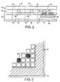
- Figure 1 is a schematic block diagram of an overall imaging configuration
- Figure 2 is a cross-section of one example of an imaging device
- Figure 3 is a schematic diagram of a plan view of corner of the image device of Figure 2.
- FIG. 4 is a schematic block diagram of an imaging configuration in accordance with an embodiment of the invention.
- Figure 5 is a flow chart for operating the configuration shown in Figure 4.
- FIG. 1 is a schematic block diagram of one example of an imaging system using an imaging device in accordance with the present invention.
- This particular embodiment is directed to the imaging of high energy radiation, for example X-ray radiation.
- high energy radiation is meant radiation having an energy in excess of approximately 1 KeV.
- the invention is by no means limited to high energy radiation such as X-rays but could be applied to the detection of any particular radiation , for example ⁇ -ray, ⁇ -ray, ⁇ -ray , infra-red or optical radiation, subject to an appropriate choice of semiconductor substrate.
- the imaging system 10 of Figure 1 is shown to provide imaging of an object 12 subject to radiation 14.
- the radiation may, for example, be X-ray radiation as mentioned above, but could alternatively be ⁇ -ray, ⁇ -ray or ⁇ -ray radiation.
- the object 12 may, for example, be part of a human body.
- the imaging device 16 comprises a plurality of image elements (here elements 18 of a two dimensional image element array).
- image elements herein elements 18 of a two dimensional image element array.
- image elements 18 of a two dimensional image element array In the following, reference will be made to image elements, although it will be appreciated that in other embodiments the individual image elements may have a configuration other than that of an element within a two dimensional array (eg a strip arrangement).
- the imaging device detects directly high energy incident radiation and accumulates at each image element, a count of the incident radiation hits at that image element.
- the imaging device can be configured as a single semiconductor substrate (eg, of silicon) with each image element comprising an image element detector 19 and image element circuitry 20.
- the imaging device 16 can be configured on two substrates, one with an array of image element detectors and one with an array of corresponding image element circuits 20, the substrates being mechanically connected to each other by, for example, conventional bump-bonding technology or any other appropriate technology.
- Figure 2 is a schematic cross section of part of an imaging device 16.
- the imaging device 16 comprises an image detector substrate 30 connected to an image circuit substrate 32 by means of bump-bonds 34.
- An image element detector 19 of each image element 18 is defined on the detector substrate 30 by a continuous electrode 36 which applies a biasing voltage and image element location electrodes 38 to define a detection zone for the image element 18.
- Corresponding image element circuits 20 on the image circuit substrate 32 are defined at locations corresponding to the electrodes 38 (ie to the image element detectors 19).
- the image element circuits 20 are electrically connected to the corresponding electrodes 38 by bump-bonds 34. In this manner, when charge is generated in an image element detector 19 in response to incident radiation, this charge is passed via the bump-bond 34 to the corresponding image element circuit 20.
- the actual size of the image element circuit and the image element detector will depend on the application for which the imaging device is intended.
- the image element detectors and image element circuits could be constructed integrally on a single semiconductor substrate. Such an implementation is possible, but sets challenges unrelated to the present invention, relating to circuit manufacturing techniques. With suitable circuit manufacturing techniques, the invention as described herein is perfectly applicable to implementation on a single semiconductor substrate, as opposed to the dual-substrate technique described herein.
- any appropriate semiconductor materials can be used for the substrates.
- silicon may be used for the detector substrate and for the image circuit substrate.
- Other semiconductor materials could be used.
- the material could be selected from: CdZnTe, CdTe, HgI 2 , InSb, GaAs, Ge, TIBr, Si and PbI.
- an electric charge is created, (or charged particle or gamma-ray is incident or absorbed for other embodiments) an electric pulse flows from image element detector 19 via the bump-bonds 34 to corresponding image element circuitry 20.
- image element circuit 20 is not relevant to the instant invention and no further description thereof shall be given, except to say that charge is accumulated within the image element circuit 20 from image element detector 19.
- Figure 2 also shows a guard ring area 48 integral with the detector substrate 30.
- the guard ring area 48 generally surrounds all the image elements 18, and may comprise several guard rings 50.
- the guard rings 50 are made from a conductive material, preferably the same material as used for image element location electrodes 38 in order for the guard rings to be fabricated at the same time as the image element electrodes 38.
- the guard ring area 48, defined by guard rings 50 reduces charge injection due to crystal defects at the edge of the detector substrate 30 by reducing the localised increase in field strength at the edge for the detector substrate 30 material.
- Continuous electrode 36 extends into the guard ring area 48 and also applies a bias voltage in the guard ring area 48. This forms a further detection zone hereinafter referred to as radiation detection cell 57, between the guard ring 48/50 and the continuous electrode 36.
- the applicant has realised that the guard ring 48/50 is exposed to radiation when the imaging device is irradiated, as well as the image element detectors 19.
- the applicant has utilised their understanding to provide a novel and inventive approach to the problems of the prior art, and to provide for self-triggering of an imaging device.
- At least one of the guard rings 50 is coupled via bump-bond 52 to output circuitry 54. Charge created by the absorption of X-ray photons is coupled from the guard ring 50 via bump-bond 52 to the output circuitry 54. Output circuitry 54 is coupled to a radiation sensor output 70.
- Figure 3 shows a corner 60 of detector substrate 30.
- Image element location electrodes 38 are disposed inside the guard ring area 48.
- radiation incident on the imaging device 16 falls not only on image element location electrodes 38, but also on guard rings 50 comprising the guard ring area 48.
- the guard ring area 48 may comprise more than one guard ring 50 for gradually reducing the field strength towards the edge of the detector substrate 30.
- the guard ring 50 is coupled to output circuitry 54 via a bump-band 52, which is directly coupled to a radiation sensor output pin on the imaging device.
- An object 66 is subject to radiation 68 from a radiation source 74.
- the radiation may be, for example, X-ray radiation, gamma-radiation, beta-ray radiation or alpha-ray radiation.
- the object 66 may be a part of the human body.
- imaging device 72 comprises a plurality of image elements in either a two or one dimensional element array or a strip arrangement, for example. Imaging device 72 is similar to imaging device 16 of Figure 1 and will be described no further, except to say that imaging device 72 comprises a guard ring 48 as described with reference to Figures 2 and 3.
- Guard ring 48 is coupled via output circuitry 54, which may be no more than a conductive path, to radiation sensor output 70.
- Radiation sensor output 70 provides a current Iguard representative of the radiation incident on the guard ring 48.
- Current Iguard is input to a current to voltage converter 78, and the resulting voltage is input to threshold circuitry 80.
- the threshold circuitry 80 has input to it a reference threshold voltage 81 (V TH ).
- the threshold circuitry 80 outputs a signal to control electronics 76 indicating that the threshold has been exceeded.
- Control electronics 76 initiates image acquisition electronics 83, and signals to the system controlling computer 84 that the threshold 81 has been exceeded, i.e. radiation incident on imaging device 72 and image acquisition has been initiated.
- Image acquisition comprises integrating the image, ie. charge on each image element, and continues until the threshold circuitry 80 indicates that the voltage has dropped below the threshold 81. That is to say, Iguard drops, indicating that the radiation source 74 has been switched off.
- the guard ring current is output, and then amplified and converted to a voltage at step 504.
- a threshold test is performed at step 506, and may be done by discrete circuitry or under program control on a digitised voltage.
- a decision is made as to whether the threshold has been exceeded. Again, such a decision may be by way of discrete circuitry included in threshold circuitry, or under the control of the suitably configured system controlling computer, for example.
- the system will continue to monitor the guard ring output, and the process returns to step 502.
- the threshold is exceeded then the image acquisition mode is initiated at step 510.
- the image is integrated whilst the image acquisition mode is active, and the guard ring output is monitored against the threshold at steps 512, 514 and 516. Whilst the threshold is exceeded, image acquisition continues and the process loops round 512, 514, 516, 518, 512...
- step 518 it is determined, that the threshold is no longer exceeded, radiation source is switched off for example, then the process goes to step 520, where the image is read out Then the process returns to step 502 begins monitoring for a new exposure.
Claims (23)
- Un dispositif à semi-conducteurs pour l'imagerie de rayonnement (72) comprenant :un réseau d'éléments d'image (18), chaque élément d'image du dit réseau comportant une cellule de détection d'élément d'image (19) qui produit une charge en réaction au rayonnement incident sur ledit élément d'image et un circuit d'éléments d'image (20) pour assurer l'accumulation de ladite charge venant de ladite cellule détectrice d'élément d'image et l'envoi sélectif d'un signal représentatif de la charge accumulée ; etun élément capteur de rayonnement (48), ledit élément capteur de rayonnement comportant une cellule de détection de rayonnement (51) intégré à un plan d'image comportant lesdites cellules de détection d'élément d'image pour produire la charge en réaction au rayonnement incident sur ledit élément capteur de rayonnement et une sortie de capteur de rayonnement pour produire en continu une charge de ladite cellule détectrice de rayonnement, dans lequel la cellule détectrice de rayonnement comporte une bague de protection (50) pour ledit réseau de cellules détectrices d'élément d'image et possède une superficie supérieure à celle de ladite cellule détectrice d'image.
- Un dispositif d'imagerie (72) conforme à la revendication 1, dans lequel ladite sortie de capteur de rayonnement est adaptée de manière à produire en continu un signal représentatif de la charge produite en réaction au rayonnement incident sur ledit élément de capteur de rayonnement (48).
- Un dispositif d'imagerie conforme à la revendication 1 ou 2, dans lequel ladite cellule détectrice de rayonnement (48) est plus sensible au rayonnement incident qu'une cellule détectrice d'élément d'image.
- Un dispositif d'imagerie (72) conforme à l'une quelconque des revendications 1 à 3, dans laquelle la bague de protection (50) est essentiellement continue.
- Un dispositif d'imagerie (72) conforme à n'importe quelle revendication précédente, comprenant un substrat unitaire (30) comprenant ladite cellule détectrice d'élément d'image, ledit circuit d'éléments d'image (20), et ladite cellule détectrice de rayonnement (51).
- Un dispositif d'imagerie (72) conforme à l'une quelconque des revendications 1 à 4, comprenant un premier substrat (30) et un second second substrat (32), le premier substrat comportant lesdites cellules détectrices d'élément d'image (19) et ladite cellule détectrice de rayonnement (51), le second substrat comportant le circuit d'éléments d'image (20).
- Un dispositif d'imagerie (72) conforme à n'importe quelle revendication précédente, comportant le circuit de seuil (80) couplé à ladite sortie de capteur de rayonnement.
- Un système d'imagerie à auto-déclenchement comportant un dispositif d'imagerie (72) conforme à l'une quelconque des revendications 1 à 6, ce système d'imagerie comportant en outre le circuit de commande (76) pour piloter le dispositif d'imagerie, un processeur d'image (84) pour traiter les valeurs de charge venant du dit réseau d'éléments d'image afin de constituer une image sur un périphérique d'affichage, et le circuit de seuil (80) couplé à ladite sortie de capteur de rayonnement
- Un système d'imagerie comportant un dispositif d'imagerie (72) conforme à la revendication 7, ce système d'imagerie comportant en outre le circuit de commande (76) pour piloter le dispositif d'imagerie, et un processeur d'images (84) pour traiter les valeurs de charge venant du dit réseau d'éléments d'image afin de constituer une image sur un périphérique d'affichage.
- Un système d'imagerie conforme à la revendication 8 ou 9, dans lequel le circuit de seuil (80) peut être mis en action de façon à émettre un signal de déclenchement au circuit de commande, pour la charge ou le signal à la sortie du capteur de rayonnement, qui dépasse une valeur de seuil (81).
- Un système d'imagerie conforme à la revendication 10, dans lequel le circuit de commande (76) peut être configuré de manière à lancer une capture d'image en réaction au dit signal de déclenchement venant du circuit de seuil (80).
- Un système d'imagerie conforme à la revendication 10 ou 11, dans lequel le circuit de commande (76) peut être configuré de manière à contrôler périodiquement le signal de déclenchement.
- Un système d'imagerie conforme à une quelconque des revendications 8 à 12, comportant en outre un convertisseur analogique-numérique pour convertir un signal analogique, fourni à la sortie du capteur de rayonnement, en une valeur numérique.
- Un système d'imagerie conforme à la revendication 13 dans lequel la valeur numérique est passée au circuit de seuil (80).
- Une méthode d'imagerie de rayonnement prévoyant la disponibilité d'un dispositif d'imagerie (72) conforme à une quelconque des revendications 1 à 7, et mettant enjeu les étapes de contrôle de ladite sortie de capteur de rayonnement, la comparaison des signaux de ladite sortie du capteur de rayonnement à un seuil (508) et l'envoi d'un signal de commande de façon à lancer la lecture du réseau, pour ladite charge ou ledit signal à la sortie du capteur de rayonnement, qui dépasse le seuil (81).
- Une méthode conforme à la revendication 15, dans laquelle l'étape de contrôle met en jeu le contrôle périodique de ladite sortie du capteur de rayonnement.
- Une méthode conforme à la revendication 15 ou 16, mettant également en jeu l'extraction d'une image (520) quand le seuil n'est plus dépassé.
- Une méthode permettant de produire un signal de déclenchement pour l'imagerie de rayonnement mettant en jeu la disponibilité d'un capteur de rayonnement, comportant une bague de protection (50), intégré à un plan d'image (30) comprenant un réseau de détecteurs de rayonnement (18) pour recueillir le rayonnement incident afin de constituer une image du rayonnement, le capteur de rayonnement étant plus sensible au rayonnement incident que l'un des détecteurs du réseau de détecteurs de rayonnement et produisant un signal indiquant un rayonnement incident sur le capteur de rayonnement, comparant le signal à un seuil (81), et envoyant un signal de commande afin de lancer une lecture du réseau (510), pour le signal du capteur de rayonnement, qui dépasse le seuil.
- Une méthode conforme à l'une quelconque des revendications 15 à 18, prévoyant en outre la disponibilité d'un circuit de commande (76) pour piloter la lecture du réseau sensible au dit signal de commande.
- Une méthode conforme à la revendication 18 ou 19 en fonction de la revendication 18, comportant en outre le contrôle périodique du dit signal de commande.
- Une méthode conforme à la revendication 18 ou à n'importe quelle revendication précédente de la revendication 16 comportant en outre la conversion d'un signal analogique indiquant un rayonnement (68) incident sur le capteur de rayonnement en une valeur numérique.
- Une méthode conforme à la revendication 18, ou à n'importe quelle revendication précédente en fonction de la revendication 18, comportant en outre la production d'une charge en réaction au rayonnement (68) incident sur l'un desdits détecteurs du réseau de détecteurs de rayonnement (18) et sur le détecteur de rayonnement (48).
- Une méthode conforme à la revendication 22, comprenant en outre le traitement des valeurs de charge mesurées sur le réseau, pour le signal du capteur de rayonnement, qui dépassent le seuil (81) afin de constituer une image sur un périphérique d'affichage.
Applications Claiming Priority (3)
| Application Number | Priority Date | Filing Date | Title |
|---|---|---|---|
| GB9806068 | 1998-03-20 | ||
| GB9806068A GB2335540B (en) | 1998-03-20 | 1998-03-20 | Imaging device for imaging radiation |
| PCT/EP1999/001282 WO1999049650A1 (fr) | 1998-03-20 | 1999-02-24 | Imageur destine a un rayonnement d'imagerie |
Publications (2)
| Publication Number | Publication Date |
|---|---|
| EP1064780A1 EP1064780A1 (fr) | 2001-01-03 |
| EP1064780B1 true EP1064780B1 (fr) | 2003-10-22 |
Family
ID=10829000
Family Applications (1)
| Application Number | Title | Priority Date | Filing Date |
|---|---|---|---|
| EP99910298A Expired - Lifetime EP1064780B1 (fr) | 1998-03-20 | 1999-02-24 | Imageur destine a un rayonnement d'imagerie |
Country Status (9)
| Country | Link |
|---|---|
| US (2) | US6380528B1 (fr) |
| EP (1) | EP1064780B1 (fr) |
| JP (1) | JP4373607B2 (fr) |
| AT (1) | ATE252804T1 (fr) |
| AU (1) | AU2930599A (fr) |
| DE (1) | DE69912259T2 (fr) |
| GB (1) | GB2335540B (fr) |
| IL (1) | IL137976A0 (fr) |
| WO (1) | WO1999049650A1 (fr) |
Families Citing this family (25)
| Publication number | Priority date | Publication date | Assignee | Title |
|---|---|---|---|---|
| IL145489A0 (en) | 1999-04-26 | 2002-06-30 | Simage Oy | Self-triggered imaging device for imaging radiation |
| GB9909572D0 (en) * | 1999-04-26 | 1999-06-23 | Simage Oy | A hardware trigger for the simage intraoral X-ray sensor |
| FR2832220B1 (fr) * | 2001-11-14 | 2004-08-27 | Univ Paris Curie | Procede et dispositif d'imagerie radiologique |
| US7223981B1 (en) * | 2002-12-04 | 2007-05-29 | Aguila Technologies Inc. | Gamma ray detector modules |
| JP2006526925A (ja) * | 2003-06-05 | 2006-11-24 | コーニンクレッカ フィリップス エレクトロニクス エヌ ヴィ | X線放射線の検出のための検出器 |
| US6928144B2 (en) * | 2003-08-01 | 2005-08-09 | General Electric Company | Guard ring for direct photo-to-electron conversion detector array |
| GB0514998D0 (en) * | 2005-07-21 | 2005-08-31 | E2V Tech Uk Ltd | Sensor with trigger pixels for imaging of pulsed radiation |
| US9087755B2 (en) * | 2007-04-24 | 2015-07-21 | Koninklijke Philips N.V. | Photodiodes and fabrication thereof |
| JP5683850B2 (ja) * | 2010-01-28 | 2015-03-11 | 富士フイルム株式会社 | 放射線検出素子、及び放射線画像撮影装置 |
| JP5475574B2 (ja) * | 2010-07-02 | 2014-04-16 | 富士フイルム株式会社 | 放射線検出素子、及び放射線画像撮影装置 |
| JP2012083307A (ja) * | 2010-10-14 | 2012-04-26 | Fujifilm Corp | 放射線検出装置、放射線画像撮影システム、放射線検出プログラム、及び放射線検出方法 |
| CN103313659B (zh) * | 2011-01-21 | 2015-11-25 | 通用电气公司 | 关于数字图像采集的x射线系统和方法 |
| US8576986B2 (en) | 2011-01-21 | 2013-11-05 | General Electric Company | X-ray system and method for sampling image data |
| US9629591B2 (en) * | 2011-01-21 | 2017-04-25 | General Electric Company | X-ray system and method with digital image acquisition |
| JP5289477B2 (ja) * | 2011-02-09 | 2013-09-11 | 富士フイルム株式会社 | 放射線画像検出装置及び放射線の照射開始検出方法 |
| US8768035B2 (en) | 2011-04-27 | 2014-07-01 | General Electric Company | X-ray system and method for processing image data |
| US9029750B1 (en) | 2011-08-02 | 2015-05-12 | Northrop Grumman Systems Corporation | CMOS and CCD sensor R/O with high gain and no kTC noise |
| KR101911314B1 (ko) | 2012-03-30 | 2018-10-24 | 삼성전자주식회사 | 엑스선 검출기 |
| DE102016203665B4 (de) | 2016-03-07 | 2020-07-09 | Siemens Healthcare Gmbh | Bestimmung eines elektrischen Gleichstromanteils im Konverterelement |
| EP3355355B1 (fr) | 2017-01-27 | 2019-03-13 | Detection Technology Oy | Contacts à anneau de garde positionnés asymétriquement |
| WO2019019041A1 (fr) * | 2017-07-26 | 2019-01-31 | Shenzhen Xpectvision Technology Co., Ltd. | Procédés de fabrication et d'utilisation de détecteurs de rayons x |
| US10813607B2 (en) * | 2018-06-27 | 2020-10-27 | Prismatic Sensors Ab | X-ray sensor, method for constructing an x-ray sensor and an x-ray imaging system comprising such an x-ray sensor |
| CN112470038A (zh) * | 2018-07-12 | 2021-03-09 | 深圳帧观德芯科技有限公司 | 辐射检测器 |
| JP7179177B2 (ja) * | 2018-11-19 | 2022-11-28 | プリズマティック、センサーズ、アクチボラグ | エッジオン光子計数検出器 |
| JP7271724B2 (ja) * | 2019-05-14 | 2023-05-11 | プリズマティック、センサーズ、アクチボラグ | フィールドリミッティングリング構成を有するx線センサ |
Family Cites Families (7)
| Publication number | Priority date | Publication date | Assignee | Title |
|---|---|---|---|---|
| US5331166A (en) * | 1991-10-25 | 1994-07-19 | Kabushiki Kaisha Morita Seisakusho | Dental X-ray image detecting device with an automatic exposure function |
| DE4300829C2 (de) * | 1993-01-14 | 1996-08-29 | Siemens Ag | Röntgendiagnostikeinrichtung |
| US5444756A (en) * | 1994-02-09 | 1995-08-22 | Minnesota Mining And Manufacturing Company | X-ray machine, solid state radiation detector and method for reading radiation detection information |
| GB2289981A (en) * | 1994-06-01 | 1995-12-06 | Simage Oy | Imaging devices systems and methods |
| FR2750821B1 (fr) * | 1996-07-05 | 1998-09-11 | Commissariat Energie Atomique | Procede et dispositif pour la prise d'images numeriques avec controle et optimisation du temps d'exposition de l'objet a des rayonnements x ou y |
| US5949848A (en) * | 1996-07-19 | 1999-09-07 | Varian Assocaites, Inc. | X-ray imaging apparatus and method using a flat amorphous silicon imaging panel |
| US5887049A (en) * | 1996-11-12 | 1999-03-23 | California Institute Of Technology | Self-triggered X-ray sensor |
-
1998
- 1998-03-20 GB GB9806068A patent/GB2335540B/en not_active Expired - Fee Related
-
1999
- 1999-02-24 DE DE69912259T patent/DE69912259T2/de not_active Expired - Lifetime
- 1999-02-24 JP JP2000538498A patent/JP4373607B2/ja not_active Expired - Lifetime
- 1999-02-24 AU AU29305/99A patent/AU2930599A/en not_active Abandoned
- 1999-02-24 WO PCT/EP1999/001282 patent/WO1999049650A1/fr active IP Right Grant
- 1999-02-24 EP EP99910298A patent/EP1064780B1/fr not_active Expired - Lifetime
- 1999-02-24 IL IL13797699A patent/IL137976A0/xx unknown
- 1999-02-24 AT AT99910298T patent/ATE252804T1/de not_active IP Right Cessation
- 1999-03-03 US US09/261,747 patent/US6380528B1/en not_active Expired - Lifetime
-
2002
- 2002-04-30 US US10/134,503 patent/US20020125438A1/en not_active Abandoned
Also Published As
| Publication number | Publication date |
|---|---|
| GB2335540A (en) | 1999-09-22 |
| IL137976A0 (en) | 2001-10-31 |
| WO1999049650A1 (fr) | 1999-09-30 |
| US6380528B1 (en) | 2002-04-30 |
| JP4373607B2 (ja) | 2009-11-25 |
| AU2930599A (en) | 1999-10-18 |
| DE69912259T2 (de) | 2004-08-05 |
| EP1064780A1 (fr) | 2001-01-03 |
| US20020125438A1 (en) | 2002-09-12 |
| GB9806068D0 (en) | 1998-05-20 |
| GB2335540B (en) | 2002-01-02 |
| ATE252804T1 (de) | 2003-11-15 |
| DE69912259D1 (de) | 2003-11-27 |
| JP2002508634A (ja) | 2002-03-19 |
Similar Documents
| Publication | Publication Date | Title |
|---|---|---|
| EP1064780B1 (fr) | Imageur destine a un rayonnement d'imagerie | |
| EP0932842B1 (fr) | Dispositif de formation d'images destine a un rayonnement d'imagerie | |
| US6797960B1 (en) | Self triggered imaging device for imaging radiation | |
| JP4989005B2 (ja) | デジタルx線撮像の方法及びセンサ装置 | |
| EP1612581B1 (fr) | Système de détection par rayons x utilisant des capteurs à pixels actifs | |
| US7361881B2 (en) | Ganged detector pixel, photon/pulse counting radiation imaging device | |
| US7566876B2 (en) | Image sensor | |
| EP1127454B1 (fr) | Dispositif d'imagerie utilisation "Time Delay Integration" et comptage de manifestation de radiation | |
| US7170065B2 (en) | Direct detection of high-energy single photons | |
| US20040212708A1 (en) | Imaging device | |
| US7501631B2 (en) | Shielding an imaging array from X-ray noise | |
| US20090108311A1 (en) | CMOS Detector with Reduced Sensitivity to X-Rays | |
| JP3361877B2 (ja) | 放射線検出器 | |
| US20140175297A1 (en) | Imaging array and method for supporting automatic exposure control in a radiographic system | |
| JP6583855B2 (ja) | 放射線検出装置 | |
| Manolopoulos et al. | X-ray imaging with photon counting hybrid semiconductor pixel detectors | |
| GB2349461A (en) | Imaging assembly for imaging radiation |
Legal Events
| Date | Code | Title | Description |
|---|---|---|---|
| PUAI | Public reference made under article 153(3) epc to a published international application that has entered the european phase |
Free format text: ORIGINAL CODE: 0009012 |
|
| 17P | Request for examination filed |
Effective date: 20000907 |
|
| AK | Designated contracting states |
Kind code of ref document: A1 Designated state(s): AT BE CH CY DE DK ES FI FR GB GR IE IT LI LU MC NL PT SE |
|
| RIN1 | Information on inventor provided before grant (corrected) |
Inventor name: ERALUOTO, MARKKU, TAPIO Inventor name: PYYHTIA, JOUNI, IIARI |
|
| 17Q | First examination report despatched |
Effective date: 20020318 |
|
| GRAH | Despatch of communication of intention to grant a patent |
Free format text: ORIGINAL CODE: EPIDOS IGRA |
|
| GRAS | Grant fee paid |
Free format text: ORIGINAL CODE: EPIDOSNIGR3 |
|
| GRAA | (expected) grant |
Free format text: ORIGINAL CODE: 0009210 |
|
| AK | Designated contracting states |
Kind code of ref document: B1 Designated state(s): AT BE CH CY DE DK ES FI FR GB GR IE IT LI LU MC NL PT SE |
|
| PG25 | Lapsed in a contracting state [announced via postgrant information from national office to epo] |
Ref country code: NL Free format text: LAPSE BECAUSE OF FAILURE TO SUBMIT A TRANSLATION OF THE DESCRIPTION OR TO PAY THE FEE WITHIN THE PRESCRIBED TIME-LIMIT Effective date: 20031022 Ref country code: LI Free format text: LAPSE BECAUSE OF FAILURE TO SUBMIT A TRANSLATION OF THE DESCRIPTION OR TO PAY THE FEE WITHIN THE PRESCRIBED TIME-LIMIT Effective date: 20031022 Ref country code: IT Free format text: LAPSE BECAUSE OF FAILURE TO SUBMIT A TRANSLATION OF THE DESCRIPTION OR TO PAY THE FEE WITHIN THE PRESCRIBED TIME-LIMIT;WARNING: LAPSES OF ITALIAN PATENTS WITH EFFECTIVE DATE BEFORE 2007 MAY HAVE OCCURRED AT ANY TIME BEFORE 2007. THE CORRECT EFFECTIVE DATE MAY BE DIFFERENT FROM THE ONE RECORDED. Effective date: 20031022 Ref country code: FR Free format text: LAPSE BECAUSE OF FAILURE TO SUBMIT A TRANSLATION OF THE DESCRIPTION OR TO PAY THE FEE WITHIN THE PRESCRIBED TIME-LIMIT Effective date: 20031022 Ref country code: FI Free format text: LAPSE BECAUSE OF FAILURE TO SUBMIT A TRANSLATION OF THE DESCRIPTION OR TO PAY THE FEE WITHIN THE PRESCRIBED TIME-LIMIT Effective date: 20031022 Ref country code: CY Free format text: LAPSE BECAUSE OF FAILURE TO SUBMIT A TRANSLATION OF THE DESCRIPTION OR TO PAY THE FEE WITHIN THE PRESCRIBED TIME-LIMIT Effective date: 20031022 Ref country code: CH Free format text: LAPSE BECAUSE OF FAILURE TO SUBMIT A TRANSLATION OF THE DESCRIPTION OR TO PAY THE FEE WITHIN THE PRESCRIBED TIME-LIMIT Effective date: 20031022 Ref country code: BE Free format text: LAPSE BECAUSE OF FAILURE TO SUBMIT A TRANSLATION OF THE DESCRIPTION OR TO PAY THE FEE WITHIN THE PRESCRIBED TIME-LIMIT Effective date: 20031022 Ref country code: AT Free format text: LAPSE BECAUSE OF FAILURE TO SUBMIT A TRANSLATION OF THE DESCRIPTION OR TO PAY THE FEE WITHIN THE PRESCRIBED TIME-LIMIT Effective date: 20031022 |
|
| REG | Reference to a national code |
Ref country code: GB Ref legal event code: FG4D |
|
| RIN1 | Information on inventor provided before grant (corrected) |
Inventor name: ERALUOTO, MARKKU, TAPIO Inventor name: PYYHTIA, JOUNI, IIARI |
|
| REG | Reference to a national code |
Ref country code: CH Ref legal event code: EP |
|
| REG | Reference to a national code |
Ref country code: IE Ref legal event code: FG4D |
|
| REF | Corresponds to: |
Ref document number: 69912259 Country of ref document: DE Date of ref document: 20031127 Kind code of ref document: P |
|
| PG25 | Lapsed in a contracting state [announced via postgrant information from national office to epo] |
Ref country code: SE Free format text: LAPSE BECAUSE OF FAILURE TO SUBMIT A TRANSLATION OF THE DESCRIPTION OR TO PAY THE FEE WITHIN THE PRESCRIBED TIME-LIMIT Effective date: 20040122 Ref country code: GR Free format text: LAPSE BECAUSE OF FAILURE TO SUBMIT A TRANSLATION OF THE DESCRIPTION OR TO PAY THE FEE WITHIN THE PRESCRIBED TIME-LIMIT Effective date: 20040122 Ref country code: DK Free format text: LAPSE BECAUSE OF FAILURE TO SUBMIT A TRANSLATION OF THE DESCRIPTION OR TO PAY THE FEE WITHIN THE PRESCRIBED TIME-LIMIT Effective date: 20040122 |
|
| PG25 | Lapsed in a contracting state [announced via postgrant information from national office to epo] |
Ref country code: ES Free format text: LAPSE BECAUSE OF FAILURE TO SUBMIT A TRANSLATION OF THE DESCRIPTION OR TO PAY THE FEE WITHIN THE PRESCRIBED TIME-LIMIT Effective date: 20040202 |
|
| PG25 | Lapsed in a contracting state [announced via postgrant information from national office to epo] |
Ref country code: LU Free format text: LAPSE BECAUSE OF NON-PAYMENT OF DUE FEES Effective date: 20040224 Ref country code: IE Free format text: LAPSE BECAUSE OF NON-PAYMENT OF DUE FEES Effective date: 20040224 Ref country code: GB Free format text: LAPSE BECAUSE OF NON-PAYMENT OF DUE FEES Effective date: 20040224 |
|
| PG25 | Lapsed in a contracting state [announced via postgrant information from national office to epo] |
Ref country code: MC Free format text: LAPSE BECAUSE OF NON-PAYMENT OF DUE FEES Effective date: 20040228 |
|
| NLV1 | Nl: lapsed or annulled due to failure to fulfill the requirements of art. 29p and 29m of the patents act | ||
| REG | Reference to a national code |
Ref country code: CH Ref legal event code: PL |
|
| PLBE | No opposition filed within time limit |
Free format text: ORIGINAL CODE: 0009261 |
|
| STAA | Information on the status of an ep patent application or granted ep patent |
Free format text: STATUS: NO OPPOSITION FILED WITHIN TIME LIMIT |
|
| 26N | No opposition filed |
Effective date: 20040723 |
|
| GBPC | Gb: european patent ceased through non-payment of renewal fee |
Effective date: 20040224 |
|
| EN | Fr: translation not filed | ||
| REG | Reference to a national code |
Ref country code: IE Ref legal event code: MM4A |
|
| PG25 | Lapsed in a contracting state [announced via postgrant information from national office to epo] |
Ref country code: PT Free format text: LAPSE BECAUSE OF NON-PAYMENT OF DUE FEES Effective date: 20040322 |
|
| REG | Reference to a national code |
Ref country code: DE Ref legal event code: R089 Ref document number: 69912259 Country of ref document: DE |
|
| REG | Reference to a national code |
Ref country code: DE Ref legal event code: R082 Ref document number: 69912259 Country of ref document: DE Ref country code: DE Ref legal event code: R082 Ref document number: 69912259 Country of ref document: DE Representative=s name: EISENFUEHR SPEISER PATENTANWAELTE RECHTSANWAEL, DE |
|
| REG | Reference to a national code |
Ref country code: DE Ref legal event code: R082 Ref document number: 69912259 Country of ref document: DE Ref country code: DE Ref legal event code: R081 Ref document number: 69912259 Country of ref document: DE Owner name: SIEMENS HEALTHCARE GMBH, DE Free format text: FORMER OWNER: IPL INTELLECTUAL PROPERTY LICENSING LTD., LIMASSOL, CY Ref country code: DE Ref legal event code: R081 Ref document number: 69912259 Country of ref document: DE Owner name: SIEMENS AKTIENGESELLSCHAFT, DE Free format text: FORMER OWNER: IPL INTELLECTUAL PROPERTY LICENSING LTD., LIMASSOL, CY |
|
| REG | Reference to a national code |
Ref country code: DE Ref legal event code: R082 Ref document number: 69912259 Country of ref document: DE Ref country code: DE Ref legal event code: R081 Ref document number: 69912259 Country of ref document: DE Owner name: SIEMENS HEALTHCARE GMBH, DE Free format text: FORMER OWNER: SIEMENS AKTIENGESELLSCHAFT, 80333 MUENCHEN, DE Ref country code: DE Ref legal event code: R081 Ref document number: 69912259 Country of ref document: DE Owner name: SIEMENS AKTIENGESELLSCHAFT, DE Free format text: FORMER OWNER: SIEMENS AKTIENGESELLSCHAFT, 80333 MUENCHEN, DE |
|
| REG | Reference to a national code |
Ref country code: DE Ref legal event code: R081 Ref document number: 69912259 Country of ref document: DE Owner name: SIEMENS HEALTHCARE GMBH, DE Free format text: FORMER OWNER: SIEMENS AKTIENGESELLSCHAFT, 80333 MUENCHEN, DE |
|
| PGFP | Annual fee paid to national office [announced via postgrant information from national office to epo] |
Ref country code: DE Payment date: 20180419 Year of fee payment: 20 |
|
| REG | Reference to a national code |
Ref country code: DE Ref legal event code: R071 Ref document number: 69912259 Country of ref document: DE |