EP1063737A2 - Method for joining wiring boards and manufacturing data carrier and device for mounting electronic component modules - Google Patents
Method for joining wiring boards and manufacturing data carrier and device for mounting electronic component modules Download PDFInfo
- Publication number
- EP1063737A2 EP1063737A2 EP00113012A EP00113012A EP1063737A2 EP 1063737 A2 EP1063737 A2 EP 1063737A2 EP 00113012 A EP00113012 A EP 00113012A EP 00113012 A EP00113012 A EP 00113012A EP 1063737 A2 EP1063737 A2 EP 1063737A2
- Authority
- EP
- European Patent Office
- Prior art keywords
- data carrier
- electronic component
- ultrasonic
- conductive
- component module
- Prior art date
- Legal status (The legal status is an assumption and is not a legal conclusion. Google has not performed a legal analysis and makes no representation as to the accuracy of the status listed.)
- Granted
Links
Images






Classifications
-
- G—PHYSICS
- G06—COMPUTING OR CALCULATING; COUNTING
- G06K—GRAPHICAL DATA READING; PRESENTATION OF DATA; RECORD CARRIERS; HANDLING RECORD CARRIERS
- G06K19/00—Record carriers for use with machines and with at least a part designed to carry digital markings
- G06K19/06—Record carriers for use with machines and with at least a part designed to carry digital markings characterised by the kind of the digital marking, e.g. shape, nature, code
- G06K19/067—Record carriers with conductive marks, printed circuits or semiconductor circuit elements, e.g. credit or identity cards also with resonating or responding marks without active components
- G06K19/07—Record carriers with conductive marks, printed circuits or semiconductor circuit elements, e.g. credit or identity cards also with resonating or responding marks without active components with integrated circuit chips
- G06K19/077—Constructional details, e.g. mounting of circuits in the carrier
- G06K19/07718—Constructional details, e.g. mounting of circuits in the carrier the record carrier being manufactured in a continuous process, e.g. using endless rolls
-
- G—PHYSICS
- G06—COMPUTING OR CALCULATING; COUNTING
- G06K—GRAPHICAL DATA READING; PRESENTATION OF DATA; RECORD CARRIERS; HANDLING RECORD CARRIERS
- G06K19/00—Record carriers for use with machines and with at least a part designed to carry digital markings
- G06K19/06—Record carriers for use with machines and with at least a part designed to carry digital markings characterised by the kind of the digital marking, e.g. shape, nature, code
- G06K19/067—Record carriers with conductive marks, printed circuits or semiconductor circuit elements, e.g. credit or identity cards also with resonating or responding marks without active components
- G06K19/07—Record carriers with conductive marks, printed circuits or semiconductor circuit elements, e.g. credit or identity cards also with resonating or responding marks without active components with integrated circuit chips
- G06K19/077—Constructional details, e.g. mounting of circuits in the carrier
- G06K19/07745—Mounting details of integrated circuit chips
-
- G—PHYSICS
- G06—COMPUTING OR CALCULATING; COUNTING
- G06K—GRAPHICAL DATA READING; PRESENTATION OF DATA; RECORD CARRIERS; HANDLING RECORD CARRIERS
- G06K19/00—Record carriers for use with machines and with at least a part designed to carry digital markings
- G06K19/06—Record carriers for use with machines and with at least a part designed to carry digital markings characterised by the kind of the digital marking, e.g. shape, nature, code
- G06K19/067—Record carriers with conductive marks, printed circuits or semiconductor circuit elements, e.g. credit or identity cards also with resonating or responding marks without active components
- G06K19/07—Record carriers with conductive marks, printed circuits or semiconductor circuit elements, e.g. credit or identity cards also with resonating or responding marks without active components with integrated circuit chips
- G06K19/077—Constructional details, e.g. mounting of circuits in the carrier
- G06K19/07749—Constructional details, e.g. mounting of circuits in the carrier the record carrier being capable of non-contact communication, e.g. constructional details of the antenna of a non-contact smart card
-
- G—PHYSICS
- G06—COMPUTING OR CALCULATING; COUNTING
- G06K—GRAPHICAL DATA READING; PRESENTATION OF DATA; RECORD CARRIERS; HANDLING RECORD CARRIERS
- G06K19/00—Record carriers for use with machines and with at least a part designed to carry digital markings
- G06K19/06—Record carriers for use with machines and with at least a part designed to carry digital markings characterised by the kind of the digital marking, e.g. shape, nature, code
- G06K19/067—Record carriers with conductive marks, printed circuits or semiconductor circuit elements, e.g. credit or identity cards also with resonating or responding marks without active components
- G06K19/07—Record carriers with conductive marks, printed circuits or semiconductor circuit elements, e.g. credit or identity cards also with resonating or responding marks without active components with integrated circuit chips
- G06K19/077—Constructional details, e.g. mounting of circuits in the carrier
- G06K19/07749—Constructional details, e.g. mounting of circuits in the carrier the record carrier being capable of non-contact communication, e.g. constructional details of the antenna of a non-contact smart card
- G06K19/0775—Constructional details, e.g. mounting of circuits in the carrier the record carrier being capable of non-contact communication, e.g. constructional details of the antenna of a non-contact smart card arrangements for connecting the integrated circuit to the antenna
-
- H—ELECTRICITY
- H01—ELECTRIC ELEMENTS
- H01R—ELECTRICALLY-CONDUCTIVE CONNECTIONS; STRUCTURAL ASSOCIATIONS OF A PLURALITY OF MUTUALLY-INSULATED ELECTRICAL CONNECTING ELEMENTS; COUPLING DEVICES; CURRENT COLLECTORS
- H01R12/00—Structural associations of a plurality of mutually-insulated electrical connecting elements, specially adapted for printed circuits, e.g. printed circuit boards [PCB], flat or ribbon cables, or like generally planar structures, e.g. terminal strips, terminal blocks; Coupling devices specially adapted for printed circuits, flat or ribbon cables, or like generally planar structures; Terminals specially adapted for contact with, or insertion into, printed circuits, flat or ribbon cables, or like generally planar structures
- H01R12/50—Fixed connections
- H01R12/51—Fixed connections for rigid printed circuits or like structures
- H01R12/52—Fixed connections for rigid printed circuits or like structures connecting to other rigid printed circuits or like structures
-
- H—ELECTRICITY
- H01—ELECTRIC ELEMENTS
- H01R—ELECTRICALLY-CONDUCTIVE CONNECTIONS; STRUCTURAL ASSOCIATIONS OF A PLURALITY OF MUTUALLY-INSULATED ELECTRICAL CONNECTING ELEMENTS; COUPLING DEVICES; CURRENT COLLECTORS
- H01R43/00—Apparatus or processes specially adapted for manufacturing, assembling, maintaining, or repairing of line connectors or current collectors or for joining electric conductors
- H01R43/02—Apparatus or processes specially adapted for manufacturing, assembling, maintaining, or repairing of line connectors or current collectors or for joining electric conductors for soldered or welded connections
- H01R43/0207—Ultrasonic-, H.F.-, cold- or impact welding
-
- H—ELECTRICITY
- H05—ELECTRIC TECHNIQUES NOT OTHERWISE PROVIDED FOR
- H05K—PRINTED CIRCUITS; CASINGS OR CONSTRUCTIONAL DETAILS OF ELECTRIC APPARATUS; MANUFACTURE OF ASSEMBLAGES OF ELECTRICAL COMPONENTS
- H05K3/00—Apparatus or processes for manufacturing printed circuits
- H05K3/36—Assembling printed circuits with other printed circuits
- H05K3/361—Assembling flexible printed circuits with other printed circuits
-
- H—ELECTRICITY
- H05—ELECTRIC TECHNIQUES NOT OTHERWISE PROVIDED FOR
- H05K—PRINTED CIRCUITS; CASINGS OR CONSTRUCTIONAL DETAILS OF ELECTRIC APPARATUS; MANUFACTURE OF ASSEMBLAGES OF ELECTRICAL COMPONENTS
- H05K2203/00—Indexing scheme relating to apparatus or processes for manufacturing printed circuits covered by H05K3/00
- H05K2203/01—Tools for processing; Objects used during processing
- H05K2203/0195—Tool for a process not provided for in H05K3/00, e.g. tool for handling objects using suction, for deforming objects, for applying local pressure
-
- H—ELECTRICITY
- H05—ELECTRIC TECHNIQUES NOT OTHERWISE PROVIDED FOR
- H05K—PRINTED CIRCUITS; CASINGS OR CONSTRUCTIONAL DETAILS OF ELECTRIC APPARATUS; MANUFACTURE OF ASSEMBLAGES OF ELECTRICAL COMPONENTS
- H05K2203/00—Indexing scheme relating to apparatus or processes for manufacturing printed circuits covered by H05K3/00
- H05K2203/02—Details related to mechanical or acoustic processing, e.g. drilling, punching, cutting, using ultrasound
- H05K2203/0285—Using ultrasound, e.g. for cleaning, soldering or wet treatment
-
- H—ELECTRICITY
- H05—ELECTRIC TECHNIQUES NOT OTHERWISE PROVIDED FOR
- H05K—PRINTED CIRCUITS; CASINGS OR CONSTRUCTIONAL DETAILS OF ELECTRIC APPARATUS; MANUFACTURE OF ASSEMBLAGES OF ELECTRICAL COMPONENTS
- H05K2203/00—Indexing scheme relating to apparatus or processes for manufacturing printed circuits covered by H05K3/00
- H05K2203/06—Lamination
- H05K2203/065—Binding insulating layers without adhesive, e.g. by local heating or welding, before lamination of the whole PCB
-
- H—ELECTRICITY
- H05—ELECTRIC TECHNIQUES NOT OTHERWISE PROVIDED FOR
- H05K—PRINTED CIRCUITS; CASINGS OR CONSTRUCTIONAL DETAILS OF ELECTRIC APPARATUS; MANUFACTURE OF ASSEMBLAGES OF ELECTRICAL COMPONENTS
- H05K3/00—Apparatus or processes for manufacturing printed circuits
- H05K3/30—Assembling printed circuits with electric components, e.g. with resistors
- H05K3/32—Assembling printed circuits with electric components, e.g. with resistors electrically connecting electric components or wires to printed circuits
- H05K3/328—Assembling printed circuits with electric components, e.g. with resistors electrically connecting electric components or wires to printed circuits by welding
-
- H—ELECTRICITY
- H10—SEMICONDUCTOR DEVICES; ELECTRIC SOLID-STATE DEVICES NOT OTHERWISE PROVIDED FOR
- H10W—GENERIC PACKAGES, INTERCONNECTIONS, CONNECTORS OR OTHER CONSTRUCTIONAL DETAILS OF DEVICES COVERED BY CLASS H10
- H10W72/00—Interconnections or connectors in packages
- H10W72/071—Connecting or disconnecting
- H10W72/072—Connecting or disconnecting of bump connectors
- H10W72/07251—Connecting or disconnecting of bump connectors characterised by changes in properties of the bump connectors during connecting
-
- H—ELECTRICITY
- H10—SEMICONDUCTOR DEVICES; ELECTRIC SOLID-STATE DEVICES NOT OTHERWISE PROVIDED FOR
- H10W—GENERIC PACKAGES, INTERCONNECTIONS, CONNECTORS OR OTHER CONSTRUCTIONAL DETAILS OF DEVICES COVERED BY CLASS H10
- H10W72/00—Interconnections or connectors in packages
- H10W72/20—Bump connectors, e.g. solder bumps or copper pillars; Dummy bumps; Thermal bumps
-
- H—ELECTRICITY
- H10—SEMICONDUCTOR DEVICES; ELECTRIC SOLID-STATE DEVICES NOT OTHERWISE PROVIDED FOR
- H10W—GENERIC PACKAGES, INTERCONNECTIONS, CONNECTORS OR OTHER CONSTRUCTIONAL DETAILS OF DEVICES COVERED BY CLASS H10
- H10W90/00—Package configurations
- H10W90/701—Package configurations characterised by the relative positions of pads or connectors relative to package parts
- H10W90/721—Package configurations characterised by the relative positions of pads or connectors relative to package parts of bump connectors
- H10W90/724—Package configurations characterised by the relative positions of pads or connectors relative to package parts of bump connectors between a chip and a stacked insulating package substrate, interposer or RDL
Definitions
- printed circuit boards 10 and 20 are joined each other by bonds such as epoxy bonding material, through-holes are made penetrating joining points 13 and 23 which are join predetermined portions, and insides of the through holes are electrically connected by metal conductive plating (such as a copper Cu) formed thereon, whereby multiple layer printed circuit boards are produced.
- bonds such as epoxy bonding material
- through-holes are made penetrating joining points 13 and 23 which are join predetermined portions, and insides of the through holes are electrically connected by metal conductive plating (such as a copper Cu) formed thereon, whereby multiple layer printed circuit boards are produced.
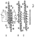
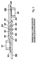
- a second embodiment of this invention In a joining method of wiring boards in this embodiment, a bonding strength by welding of conductive metals is strengthened by the welding strength between board resins.
- the conductive patterns 102 and 202 commonly employ metal conductor of copper or aluminum of 10 to 36 micrometers in thickness, whereby sufficient mechanical strength cannot be expected in the welding between these metal foils. This disadvantage may be overcome by this second embodiment.
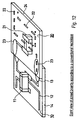
- Fig. 5 shows a top view of a whole construction of a data carrier 400
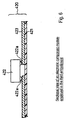
- Fig. 6 shows an enlarged sectional view of one example of construction of an electronic component module 420 including a gold bump 422a and an aluminum conductive pattern 423
- the data carrier 400 includes a data carrier body 410 in which a copper foil spiral conductive pattern 412 (serving as an antenna) having a thickness of 10 micrometers held on one wall of PET (ethylene resin naphtha rate) board 411 having a thickness of 25 micrometers, and the electronic component module 420 in which a PET film small piece 421 having a thickness of 25 micrometers including an aluminum wiring conductive pattern 423 on a surface thereof is mounted by an electronic component, pair chip IC 422.
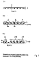
- an etching resist pattern 4 including a spiral shape and a terminal shape is formed on a surface of the copper foil 3 of the Cu-PET laminating member 1.
- insulating etching resist ink is printed on the copper foil by offset printing in a spiral shape having a turn number, a lead width, a pitch and inner and outer circumferences to provide an L value and a Q value which are necessary for characteristics of the coil.
- the resist ink is employed to be hardened by heat or activation energy rays.
- the activation energy rays employ an ultra-violet ray or electron beam. When the ultra-violet ray is employed, the resist ink is used by putting photo polymerization materials therein.
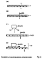
- An electronic component 8 (422) is mounted on a conductive pattern 6a formed on the PET film 5 to complete an electronic component module 420.
- the electronic component 8 is constructed to have gold bumps 8a from a bottom wall thereof for connection as a surface mount type component.
- the gold bumps 8a projecting from the bottom wall are loaded by ultrasonic wave vibrations to mechanically remove the oxidate layer on a surface of the aluminum conductive pattern 6a, and further by heat caused by frictional heat to disperse gold atoms within the aluminum for junction.
- this mounting method is executed by applying an ultrasonic wave vibration of 40KHz for several seconds under load pressure 0.2Kg/mm 2 (Process D).
- the base member in this embodiment employs an ethylene resin naphtha rate (PET) film, but may employ a polyimide film or the like, if desired.
- Anvils 11 and 12 are arranged to opposite to the penetrators 9 and 10.
- welding is performed by approaching atoms into a distance (several angstroms) where attractive forces work in mutual atoms on surfaces of metals to be joined and arranging atoms over the surface in order to be contacted.
- the surface of metals are covered with a thin layer of oxidate and adsorption gas, whereby clean metal atoms on the lower layer are prevented from approaching and sufficient joining force is not produced.
Landscapes
- Engineering & Computer Science (AREA)
- Microelectronics & Electronic Packaging (AREA)
- Computer Hardware Design (AREA)
- Physics & Mathematics (AREA)
- General Physics & Mathematics (AREA)
- Theoretical Computer Science (AREA)
- Manufacturing & Machinery (AREA)
- Pressure Welding/Diffusion-Bonding (AREA)
- Combinations Of Printed Boards (AREA)
- Wire Bonding (AREA)
Abstract
Description
Thus, according to this invention, joining of this kind of wiring boards is performed at a reduced cost and for a short time, and may be applied to the boards after mounting electronic components thereon.
Claims (5)
- A method for joining a first wiring board (100) covered with a conductive pattern (102) on a surface of a thin resin basic plate (104) to a second wiring board (200) covered with a conductive pattern (202) on a thin resin basic plate (204) to ensure the electric connection therebetween, comprising the steps ofputting said first and second wiring boards (100 and 200) together in a confront relationship so as to adjust join predetermined portions (103 and 203) on the conductive patterns,catching the join predetermined portions (103 and 203) in the status by a pair of ultrasonic welding tools (40 and 41), andapplying an ultrasonic vibration to said ultrasonic welding tools (40 or 41) to weld the conductive metals located on the join predetermined portions (103 and 203).
- A method for joining the wiring boards according to claim 1, in which a plurality of projections (41a) each having an end face shape corresponding to a desired welding portion shape are disposed on at least one of opposite end faces of said pair of ultrasonic welding tools (40 and 41), further comprising the steps of partially removing a conductive metal due to plasticity flow (a) of the metal when an ultrasonic vibration is applied by said projections (41a), and welding resins (104 and 204) exposed by the removed portion (b).
- A method for manufacturing a film-type data carrier (400) by joining an electronic component module (420) in which a conductive pattern (423) is adhered on a surface of a film-type resin small piece (421) and electronic components (422), providing a transmission and reception circuit, and a memory mounted thereon, to a data carrier body (410) having a spiral conductive pattern (412) providing an antenna adhered on a surface of a film-type resin base plate (411), to be unified to ensure an electrical conduction for reading electromagnetic waves, comprising the steps ofputting said film-type resin base plate (411) of the data carrier body (410) and said film-type resin small piece (421) of the electronic component module (420) together in a face-to-face relationship to adjust join predetermined portions (6a-1, 6a-2, 414 and 415) on the conductive patterns (6a and 3),catching the adjusted join predetermined portions (6a-1, 6a-2, 414 and 415) by a pair of ultrasonic welding tools (9, 10, 11 and 12), andapplying an ultrasonic vibration to said ultrasonic welding tools (9, 10, 11 and 12) to weld the conductive metals located on the join predetermined portions (6a-1, 6a-2, 414 and 415).
- A method for manufacturing a data carrier according to claim 3 in which a plurality of projections (41a) each having end face shape corresponding to a desired welding portion shape are disposed on at least one of opposite end faces of said ultrasonic welding tools (9, 10, 11 and 12), further comprising the steps of partially removing conductive metal due to plasticity flow of the metal when an ultrasonic vibration is applied by the plurality of projections, and welding plastics exposed by the removed portion.
- An electronic component module mounting device (500) for mounting an electronic component module (420) on a data carrier body in a manufacturing process for an electromagnetic wave readable film-type data carrier, comprisinga punch work die (503) having a mold configuration corresponding to the electronic component module,a punch (507) to be inserted into said punch work die (503),a support table (505) disposed opposing to a punching forward direction of said die to push said data carrier body (504) backward, andan ultrasonic horn (506) applying ultrasonic wave vibrations to said punch (507), in which the electronic component module (420) is punched out from an electronic component mounting film base (509) by the die and the punch (507), said punched out electronic component module (420) is pushed to the data carrier body (504) in proportion to the forward movement of said punch (507) to be welded on said data carrier body (504) by applying ultrasonic wave vibrations to said punch (507) by driving said ultrasonic horn (506).
Applications Claiming Priority (2)
| Application Number | Priority Date | Filing Date | Title |
|---|---|---|---|
| JP17602299A JP3928682B2 (en) | 1999-06-22 | 1999-06-22 | Wiring board bonded body, wiring board bonding method, data carrier manufacturing method, and electronic component module mounting apparatus |
| JP17602299 | 1999-06-22 |
Publications (3)
| Publication Number | Publication Date |
|---|---|
| EP1063737A2 true EP1063737A2 (en) | 2000-12-27 |
| EP1063737A3 EP1063737A3 (en) | 2005-06-08 |
| EP1063737B1 EP1063737B1 (en) | 2009-01-07 |
Family
ID=16006364
Family Applications (1)
| Application Number | Title | Priority Date | Filing Date |
|---|---|---|---|
| EP00113012A Expired - Lifetime EP1063737B1 (en) | 1999-06-22 | 2000-06-21 | Method for manufacturing a film-type data carrier |
Country Status (4)
| Country | Link |
|---|---|
| US (1) | US6523734B1 (en) |
| EP (1) | EP1063737B1 (en) |
| JP (1) | JP3928682B2 (en) |
| DE (1) | DE60041302D1 (en) |
Cited By (4)
| Publication number | Priority date | Publication date | Assignee | Title |
|---|---|---|---|---|
| EP1447166A1 (en) * | 2003-02-17 | 2004-08-18 | Carl Freudenberg KG | Method and apparatus for joining at least two metal foils by welding and such joints |
| EP1538559A1 (en) * | 2003-11-12 | 2005-06-08 | Hitachi, Ltd. | Method of manufacturing RFID |
| US7361251B2 (en) | 2002-01-18 | 2008-04-22 | Avery Dennison Corporation | RFID label technique |
| WO2017092907A1 (en) * | 2015-12-03 | 2017-06-08 | Continental Teves Ag & Co. Ohg | Electric conductor track, method, and use |
Families Citing this family (54)
| Publication number | Priority date | Publication date | Assignee | Title |
|---|---|---|---|---|
| US6468638B2 (en) * | 1999-03-16 | 2002-10-22 | Alien Technology Corporation | Web process interconnect in electronic assemblies |
| US6606247B2 (en) * | 2001-05-31 | 2003-08-12 | Alien Technology Corporation | Multi-feature-size electronic structures |
| US7218527B1 (en) * | 2001-08-17 | 2007-05-15 | Alien Technology Corporation | Apparatuses and methods for forming smart labels |
| MY134549A (en) * | 2001-12-10 | 2007-12-31 | Hitachi Chemical Co Ltd | Film lamination method and lamination apparatus |
| US7214569B2 (en) * | 2002-01-23 | 2007-05-08 | Alien Technology Corporation | Apparatus incorporating small-feature-size and large-feature-size components and method for making same |
| JP3739752B2 (en) * | 2003-02-07 | 2006-01-25 | 株式会社 ハリーズ | Small-piece transfer device capable of random-cycle shifting |
| US7253735B2 (en) | 2003-03-24 | 2007-08-07 | Alien Technology Corporation | RFID tags and processes for producing RFID tags |
| US7285447B2 (en) * | 2003-06-25 | 2007-10-23 | Intel Corporation | Method and apparatus for imprinting a circuit pattern using ultrasonic vibrations |
| US20050109746A1 (en) * | 2003-11-26 | 2005-05-26 | International Business Machines Corporation | Method for fluxless soldering of workpieces |
| JP4526813B2 (en) * | 2003-12-16 | 2010-08-18 | 株式会社フジクラ | Manufacturing method of joined body |
| JP4526814B2 (en) * | 2003-12-18 | 2010-08-18 | 株式会社フジクラ | Manufacturing method of joined body |
| JP4251104B2 (en) * | 2004-03-31 | 2009-04-08 | 株式会社日立製作所 | RFID tag manufacturing method |
| US20060109130A1 (en) * | 2004-11-22 | 2006-05-25 | Hattick John B | Radio frequency identification (RFID) tag for an item having a conductive layer included or attached |
| US7385284B2 (en) * | 2004-11-22 | 2008-06-10 | Alien Technology Corporation | Transponder incorporated into an electronic device |
| US7688206B2 (en) | 2004-11-22 | 2010-03-30 | Alien Technology Corporation | Radio frequency identification (RFID) tag for an item having a conductive layer included or attached |
| EP1835796B9 (en) * | 2004-12-03 | 2011-02-23 | Hallys Corporation | Interposer bonding device |
| EP1833290A4 (en) * | 2004-12-03 | 2009-11-11 | Hallys Corp | METHOD FOR MANUFACTURING ELECTRONIC COMPONENT AND EQUIPMENT FOR MANUFACTURING ELECTRONIC COMPONENT |
| JP4810531B2 (en) | 2005-04-06 | 2011-11-09 | 株式会社 ハリーズ | Electronic component manufacturing equipment |
| US20090166431A1 (en) * | 2005-04-18 | 2009-07-02 | Hallys Corporation | Electronic component and manufacturing method thereof |
| US7623034B2 (en) | 2005-04-25 | 2009-11-24 | Avery Dennison Corporation | High-speed RFID circuit placement method and device |
| DE102005035102A1 (en) * | 2005-07-27 | 2007-02-01 | Robert Bosch Gmbh | Electrically conductive connection and method for producing such |
| WO2007030768A2 (en) * | 2005-09-09 | 2007-03-15 | Delaware Capital Formation, Inc. | Strap/inlay insertion method and apparatus |
| JP2007226518A (en) * | 2006-02-23 | 2007-09-06 | Dainippon Printing Co Ltd | IC tag and manufacturing method of IC tag |
| JP5017358B2 (en) * | 2006-03-28 | 2012-09-05 | シーアールシー フォー アドバンスト コンポジット ストラクチャーズ リミテッド | Welding of functional members to polymer composite members |
| WO2007125939A1 (en) * | 2006-04-27 | 2007-11-08 | Neomax Materials Co., Ltd. | Clad material for wiring connection and wiring connection member processed from the clad material |
| JP4967467B2 (en) * | 2006-06-12 | 2012-07-04 | 富士通株式会社 | Flexible wiring board bonding method and wiring board |
| US7901533B2 (en) * | 2006-06-30 | 2011-03-08 | Tamarack Products, Inc. | Method of making an RFID article |
| DE102007001411A1 (en) | 2007-01-09 | 2008-07-10 | Mühlbauer Ag | Method for manufacturing electronic data carrier, involves arranging electronic component module exchange areas to exchange areas of wire or thread |
| WO2008088984A2 (en) | 2007-01-11 | 2008-07-24 | University Of Pittsburgh - Of The Commonwealth System Of Higher Education | Transponder networks and transponder systems employing a touch probe reader device |
| EP2001077A1 (en) * | 2007-05-21 | 2008-12-10 | Gemplus | Method of manufacturing a device comprising a transponder antenna connected to connecting pads and device obtained |
| US8062445B2 (en) * | 2007-08-06 | 2011-11-22 | Avery Dennison Corporation | Method of making RFID devices |
| JP5247571B2 (en) * | 2008-04-24 | 2013-07-24 | パナソニック株式会社 | Wiring board and wiring board connection method |
| JP5171405B2 (en) * | 2008-06-05 | 2013-03-27 | 株式会社 ハリーズ | Interposer joining method |
| CN102047404B (en) * | 2008-12-16 | 2013-07-10 | 松下电器产业株式会社 | Semiconductor device, flip-chip mounting method and flip-chip mounting apparatus |
| JP5799501B2 (en) * | 2010-06-24 | 2015-10-28 | 日産自動車株式会社 | Joining method and joining apparatus |
| DE112011102493B4 (en) * | 2010-07-26 | 2021-11-04 | Pukyong National University Business Incubator Center | Device for vibro spot welding |
| JP5644286B2 (en) * | 2010-09-07 | 2014-12-24 | オムロン株式会社 | Electronic component surface mounting method and electronic component mounted substrate |
| US20120107546A1 (en) * | 2010-10-28 | 2012-05-03 | Gm Global Technology Operations, Inc. | Coulomb damping and/or viscous damping insert using ultrasonic welding |
| US9522514B2 (en) | 2013-12-19 | 2016-12-20 | Intel Corporation | Substrate or panel with releasable core |
| US9554468B2 (en) | 2013-12-19 | 2017-01-24 | Intel Corporation | Panel with releasable core |
| US9434135B2 (en) | 2013-12-19 | 2016-09-06 | Intel Corporation | Panel with releasable core |
| US9554472B2 (en) * | 2013-12-19 | 2017-01-24 | Intel Corporation | Panel with releasable core |
| JP2016054040A (en) * | 2014-09-03 | 2016-04-14 | セイコーインスツル株式会社 | Electronic device and method of manufacturing the same |
| JP6265310B2 (en) | 2015-10-02 | 2018-01-24 | 株式会社村田製作所 | Resin substrate structure and manufacturing method thereof |
| US9981336B2 (en) * | 2015-11-04 | 2018-05-29 | Kulicke And Soffa Industries, Inc. | Ribbon bonding tools, and methods of designing ribbon bonding tools |
| CN108883492A (en) * | 2016-03-18 | 2018-11-23 | 本田技研工业株式会社 | Ultrasonic bonding equipment and ultrasonic connection method |
| WO2017159329A1 (en) * | 2016-03-18 | 2017-09-21 | 本田技研工業株式会社 | Ultrasonic welding device and ultrasonic welding method |
| CN109526212B (en) * | 2016-08-04 | 2021-03-23 | 东芝三菱电机产业系统株式会社 | Ultrasonic bonding tool and ultrasonic bonding device |
| JP2019013959A (en) * | 2017-07-06 | 2019-01-31 | イーグル工業株式会社 | Ultrasonic joining jig, joining structure and joining method |
| WO2019068068A1 (en) * | 2017-09-29 | 2019-04-04 | Avery Dennison Retail Information Services, Llc | Strap mounting techniques for wire format antennas |
| WO2019068077A1 (en) | 2017-09-29 | 2019-04-04 | Avery Dennison Retail Information Services, Llc | Systems and methods for transferring a flexible conductor onto a moving web |
| JP6785210B2 (en) * | 2017-11-28 | 2020-11-18 | 矢崎総業株式会社 | Ultrasonic bonding method for electric wire conductors, manufacturing method for electric wires with terminals, and ultrasonic bonding equipment |
| US12651880B2 (en) * | 2021-04-12 | 2026-06-09 | St. Jude Medical, Cardiology Division, Inc. | Ultrasonically bonding a flexible electronic circuit element having a plurality of vias |
| WO2024027891A1 (en) * | 2022-08-01 | 2024-02-08 | Hitachi Energy Ltd | Method for attaching a terminal to a metal substrate structure for a semiconductor power module and semiconductor power module |
Family Cites Families (7)
| Publication number | Priority date | Publication date | Assignee | Title |
|---|---|---|---|---|
| US3934783A (en) * | 1974-09-30 | 1976-01-27 | Larrison John E | Multiface wire bonding method and tool |
| JPH05121139A (en) * | 1991-10-24 | 1993-05-18 | Sumitomo Wiring Syst Ltd | Connecting method for flat conductor |
| US5354392A (en) * | 1992-01-24 | 1994-10-11 | Matsushita Electric Industrial Co., Ltd. | Method for connecting a wiring arranged on a sheet with another wiring arranged on another sheet by ultrasonic waves |
| DE19500925C2 (en) * | 1995-01-16 | 1999-04-08 | Orga Kartensysteme Gmbh | Method for producing a contactless chip card |
| JPH0952185A (en) * | 1995-08-14 | 1997-02-25 | Yazaki Corp | Ultrasonic welding machine |
| FR2743649B1 (en) * | 1996-01-17 | 1998-04-03 | Gemplus Card Int | CONTACTLESS ELECTRONIC MODULE, ELECTRONIC LABEL CARD INCORPORATING THE SAME, AND METHODS OF MAKING SAME |
| DE19846237A1 (en) * | 1998-10-07 | 2000-04-13 | Fraunhofer Ges Forschung | Process for the production of a microtransponder |
-
1999
- 1999-06-22 JP JP17602299A patent/JP3928682B2/en not_active Expired - Lifetime
-
2000
- 2000-06-09 US US09/591,346 patent/US6523734B1/en not_active Expired - Lifetime
- 2000-06-21 DE DE60041302T patent/DE60041302D1/en not_active Expired - Lifetime
- 2000-06-21 EP EP00113012A patent/EP1063737B1/en not_active Expired - Lifetime
Cited By (6)
| Publication number | Priority date | Publication date | Assignee | Title |
|---|---|---|---|---|
| US7361251B2 (en) | 2002-01-18 | 2008-04-22 | Avery Dennison Corporation | RFID label technique |
| EP1447166A1 (en) * | 2003-02-17 | 2004-08-18 | Carl Freudenberg KG | Method and apparatus for joining at least two metal foils by welding and such joints |
| FR2851186A1 (en) * | 2003-02-17 | 2004-08-20 | Meillor Sa | METHOD AND DEVICE FOR JOINING BY WELDING AT LEAST TWO METAL SHEETS AND JOINTS OBTAINED |
| EP1538559A1 (en) * | 2003-11-12 | 2005-06-08 | Hitachi, Ltd. | Method of manufacturing RFID |
| WO2017092907A1 (en) * | 2015-12-03 | 2017-06-08 | Continental Teves Ag & Co. Ohg | Electric conductor track, method, and use |
| US10438871B2 (en) | 2015-12-03 | 2019-10-08 | Continental Teves Ag & Co. Ohg | Electric conductor track, method, and use |
Also Published As
| Publication number | Publication date |
|---|---|
| EP1063737B1 (en) | 2009-01-07 |
| DE60041302D1 (en) | 2009-02-26 |
| US6523734B1 (en) | 2003-02-25 |
| EP1063737A3 (en) | 2005-06-08 |
| JP3928682B2 (en) | 2007-06-13 |
| JP2001007511A (en) | 2001-01-12 |
Similar Documents
| Publication | Publication Date | Title |
|---|---|---|
| US6523734B1 (en) | Method for joining wiring boards and manufacturing data carrier and device for mounting electronic component modules | |
| US6664645B2 (en) | Method of mounting a semiconductor chip, circuit board for flip-chip connection and method of manufacturing the same, electromagnetic wave readable data carrier and method of manufacturing the same, and electronic component module for an electromagnetic wave readable data carrier | |
| US7214569B2 (en) | Apparatus incorporating small-feature-size and large-feature-size components and method for making same | |
| US6908318B2 (en) | Batch electrically connecting sheet | |
| US6243946B1 (en) | Method of forming an interlayer connection structure | |
| JP2004095566A (en) | SHIELD FILM, SHIELD FLEXIBLE PRINTED WIRING BOARD AND PROCESS FOR PRODUCING THEM | |
| CN100358119C (en) | Method of manufacturing RFID | |
| JP5155616B2 (en) | RFID tag, RFID system, and RFID tag manufacturing method | |
| CN101772259B (en) | Printed wiring board, method of manufacturing printed wiring board, and method of connecting printed wiring board | |
| JP2007110010A (en) | Flexible printed wiring board, flexible printed circuit board, and manufacturing method thereof | |
| EP1415369B1 (en) | Batch electrically connecting sheet | |
| JPH11112150A (en) | Multilayer substrate and manufacturing method thereof | |
| JP3463539B2 (en) | Flexible circuit board with anisotropic conductive adhesive and manufacturing method | |
| JP2000090226A (en) | IC module manufacturing method and IC card manufacturing method | |
| JPH11328355A (en) | IC module for IC card | |
| JP2003203946A (en) | Semiconductor chip mounting method | |
| JP2003069216A (en) | Connection method between conductive connection parts | |
| JP2002259923A (en) | Non-contact IC card and method of manufacturing the same | |
| EP1983808A1 (en) | Method for manufacturing tape carrier for contact type IC card | |
| JP2007012700A (en) | Laminated sheet circuit wiring module and IC tag internal circuit connection structure | |
| JPH06318785A (en) | Method for manufacturing multilayer wiring board | |
| JP2002016110A (en) | Semiconductor device | |
| JP2001250604A (en) | Method for manufacturing conductive sheet and printed circuit board | |
| JPS6372186A (en) | Manufacture of printed wiring board |
Legal Events
| Date | Code | Title | Description |
|---|---|---|---|
| PUAI | Public reference made under article 153(3) epc to a published international application that has entered the european phase |
Free format text: ORIGINAL CODE: 0009012 |
|
| AK | Designated contracting states |
Kind code of ref document: A2 Designated state(s): AT BE CH CY DE DK ES FI FR GB GR IE IT LI LU MC NL PT SE |
|
| AX | Request for extension of the european patent |
Free format text: AL;LT;LV;MK;RO;SI |
|
| PUAL | Search report despatched |
Free format text: ORIGINAL CODE: 0009013 |
|
| AK | Designated contracting states |
Kind code of ref document: A3 Designated state(s): AT BE CH CY DE DK ES FI FR GB GR IE IT LI LU MC NL PT SE |
|
| AX | Request for extension of the european patent |
Extension state: AL LT LV MK RO SI |
|
| RIC1 | Information provided on ipc code assigned before grant |
Ipc: 7H 01R 43/02 B Ipc: 7H 05K 3/36 A Ipc: 7G 06K 19/077 B |
|
| RIN1 | Information on inventor provided before grant (corrected) |
Inventor name: OKADA, MASANOBU Inventor name: KAWAI, WAKAHIRO |
|
| 17P | Request for examination filed |
Effective date: 20051130 |
|
| AKX | Designation fees paid |
Designated state(s): DE FR GB IT |
|
| GRAP | Despatch of communication of intention to grant a patent |
Free format text: ORIGINAL CODE: EPIDOSNIGR1 |
|
| RTI1 | Title (correction) |
Free format text: METHOD FOR MANUFACTURING A FILM-TYPE DATA CARRIER |
|
| GRAS | Grant fee paid |
Free format text: ORIGINAL CODE: EPIDOSNIGR3 |
|
| GRAA | (expected) grant |
Free format text: ORIGINAL CODE: 0009210 |
|
| AK | Designated contracting states |
Kind code of ref document: B1 Designated state(s): DE FR GB IT |
|
| REG | Reference to a national code |
Ref country code: GB Ref legal event code: FG4D |
|
| REF | Corresponds to: |
Ref document number: 60041302 Country of ref document: DE Date of ref document: 20090226 Kind code of ref document: P |
|
| PLBE | No opposition filed within time limit |
Free format text: ORIGINAL CODE: 0009261 |
|
| STAA | Information on the status of an ep patent application or granted ep patent |
Free format text: STATUS: NO OPPOSITION FILED WITHIN TIME LIMIT |
|
| 26N | No opposition filed |
Effective date: 20091008 |
|
| PG25 | Lapsed in a contracting state [announced via postgrant information from national office to epo] |
Ref country code: IT Free format text: LAPSE BECAUSE OF FAILURE TO SUBMIT A TRANSLATION OF THE DESCRIPTION OR TO PAY THE FEE WITHIN THE PRESCRIBED TIME-LIMIT Effective date: 20090107 |
|
| PGFP | Annual fee paid to national office [announced via postgrant information from national office to epo] |
Ref country code: FR Payment date: 20110621 Year of fee payment: 12 |
|
| PGFP | Annual fee paid to national office [announced via postgrant information from national office to epo] |
Ref country code: GB Payment date: 20110615 Year of fee payment: 12 |
|
| PGFP | Annual fee paid to national office [announced via postgrant information from national office to epo] |
Ref country code: DE Payment date: 20110615 Year of fee payment: 12 |
|
| GBPC | Gb: european patent ceased through non-payment of renewal fee |
Effective date: 20120621 |
|
| REG | Reference to a national code |
Ref country code: FR Ref legal event code: ST Effective date: 20130228 |
|
| REG | Reference to a national code |
Ref country code: DE Ref legal event code: R119 Ref document number: 60041302 Country of ref document: DE Effective date: 20130101 |
|
| PG25 | Lapsed in a contracting state [announced via postgrant information from national office to epo] |
Ref country code: FR Free format text: LAPSE BECAUSE OF NON-PAYMENT OF DUE FEES Effective date: 20120702 Ref country code: DE Free format text: LAPSE BECAUSE OF NON-PAYMENT OF DUE FEES Effective date: 20130101 Ref country code: GB Free format text: LAPSE BECAUSE OF NON-PAYMENT OF DUE FEES Effective date: 20120621 |