EP1063687A2 - Titanium-tantalum barrier layer film and method for forming the same - Google Patents
Titanium-tantalum barrier layer film and method for forming the same Download PDFInfo
- Publication number
- EP1063687A2 EP1063687A2 EP00304061A EP00304061A EP1063687A2 EP 1063687 A2 EP1063687 A2 EP 1063687A2 EP 00304061 A EP00304061 A EP 00304061A EP 00304061 A EP00304061 A EP 00304061A EP 1063687 A2 EP1063687 A2 EP 1063687A2
- Authority
- EP
- European Patent Office
- Prior art keywords
- titanium
- film
- tantalum
- barrier layer
- sputtering
- Prior art date
- Legal status (The legal status is an assumption and is not a legal conclusion. Google has not performed a legal analysis and makes no representation as to the accuracy of the status listed.)
- Withdrawn
Links
Images

Classifications
-
- H—ELECTRICITY
- H10—SEMICONDUCTOR DEVICES; ELECTRIC SOLID-STATE DEVICES NOT OTHERWISE PROVIDED FOR
- H10W—GENERIC PACKAGES, INTERCONNECTIONS, CONNECTORS OR OTHER CONSTRUCTIONAL DETAILS OF DEVICES COVERED BY CLASS H10
- H10W20/00—Interconnections in chips, wafers or substrates
- H10W20/01—Manufacture or treatment
- H10W20/031—Manufacture or treatment of conductive parts of the interconnections
- H10W20/032—Manufacture or treatment of conductive parts of the interconnections of conductive barrier, adhesion or liner layers
- H10W20/052—Manufacture or treatment of conductive parts of the interconnections of conductive barrier, adhesion or liner layers by treatments not introducing additional elements therein
- H10W20/0526—Manufacture or treatment of conductive parts of the interconnections of conductive barrier, adhesion or liner layers by treatments not introducing additional elements therein by thermal treatment thereof
-
- H—ELECTRICITY
- H10—SEMICONDUCTOR DEVICES; ELECTRIC SOLID-STATE DEVICES NOT OTHERWISE PROVIDED FOR
- H10W—GENERIC PACKAGES, INTERCONNECTIONS, CONNECTORS OR OTHER CONSTRUCTIONAL DETAILS OF DEVICES COVERED BY CLASS H10
- H10W20/00—Interconnections in chips, wafers or substrates
- H10W20/01—Manufacture or treatment
- H10W20/031—Manufacture or treatment of conductive parts of the interconnections
- H10W20/032—Manufacture or treatment of conductive parts of the interconnections of conductive barrier, adhesion or liner layers
-
- H—ELECTRICITY
- H10—SEMICONDUCTOR DEVICES; ELECTRIC SOLID-STATE DEVICES NOT OTHERWISE PROVIDED FOR
- H10W—GENERIC PACKAGES, INTERCONNECTIONS, CONNECTORS OR OTHER CONSTRUCTIONAL DETAILS OF DEVICES COVERED BY CLASS H10
- H10W20/00—Interconnections in chips, wafers or substrates
- H10W20/01—Manufacture or treatment
- H10W20/031—Manufacture or treatment of conductive parts of the interconnections
- H10W20/032—Manufacture or treatment of conductive parts of the interconnections of conductive barrier, adhesion or liner layers
- H10W20/033—Manufacture or treatment of conductive parts of the interconnections of conductive barrier, adhesion or liner layers in openings in dielectrics
-
- H—ELECTRICITY
- H10—SEMICONDUCTOR DEVICES; ELECTRIC SOLID-STATE DEVICES NOT OTHERWISE PROVIDED FOR
- H10W—GENERIC PACKAGES, INTERCONNECTIONS, CONNECTORS OR OTHER CONSTRUCTIONAL DETAILS OF DEVICES COVERED BY CLASS H10
- H10W20/00—Interconnections in chips, wafers or substrates
- H10W20/01—Manufacture or treatment
- H10W20/031—Manufacture or treatment of conductive parts of the interconnections
- H10W20/032—Manufacture or treatment of conductive parts of the interconnections of conductive barrier, adhesion or liner layers
- H10W20/033—Manufacture or treatment of conductive parts of the interconnections of conductive barrier, adhesion or liner layers in openings in dielectrics
- H10W20/035—Manufacture or treatment of conductive parts of the interconnections of conductive barrier, adhesion or liner layers in openings in dielectrics combinations of barrier, adhesion or liner layers, e.g. multi-layered barrier layers
-
- H—ELECTRICITY
- H10—SEMICONDUCTOR DEVICES; ELECTRIC SOLID-STATE DEVICES NOT OTHERWISE PROVIDED FOR
- H10W—GENERIC PACKAGES, INTERCONNECTIONS, CONNECTORS OR OTHER CONSTRUCTIONAL DETAILS OF DEVICES COVERED BY CLASS H10
- H10W20/00—Interconnections in chips, wafers or substrates
- H10W20/40—Interconnections external to wafers or substrates, e.g. back-end-of-line [BEOL] metallisations or vias connecting to gate electrodes
- H10W20/41—Interconnections external to wafers or substrates, e.g. back-end-of-line [BEOL] metallisations or vias connecting to gate electrodes characterised by their conductive parts
- H10W20/425—Barrier, adhesion or liner layers
-
- H—ELECTRICITY
- H10—SEMICONDUCTOR DEVICES; ELECTRIC SOLID-STATE DEVICES NOT OTHERWISE PROVIDED FOR
- H10W—GENERIC PACKAGES, INTERCONNECTIONS, CONNECTORS OR OTHER CONSTRUCTIONAL DETAILS OF DEVICES COVERED BY CLASS H10
- H10W20/00—Interconnections in chips, wafers or substrates
- H10W20/01—Manufacture or treatment
- H10W20/031—Manufacture or treatment of conductive parts of the interconnections
- H10W20/032—Manufacture or treatment of conductive parts of the interconnections of conductive barrier, adhesion or liner layers
- H10W20/0375—Manufacture or treatment of conductive parts of the interconnections of conductive barrier, adhesion or liner layers comprising multiple stacked thin barrier, adhesion or liner layers not being formed in openings in dielectrics
-
- H—ELECTRICITY
- H10—SEMICONDUCTOR DEVICES; ELECTRIC SOLID-STATE DEVICES NOT OTHERWISE PROVIDED FOR
- H10W—GENERIC PACKAGES, INTERCONNECTIONS, CONNECTORS OR OTHER CONSTRUCTIONAL DETAILS OF DEVICES COVERED BY CLASS H10
- H10W20/00—Interconnections in chips, wafers or substrates
- H10W20/01—Manufacture or treatment
- H10W20/071—Manufacture or treatment of dielectric parts thereof
- H10W20/081—Manufacture or treatment of dielectric parts thereof by forming openings in the dielectric parts
- H10W20/084—Manufacture or treatment of dielectric parts thereof by forming openings in the dielectric parts for dual-damascene structures
Definitions
- the present invention relates generally to semiconductor integrated circuit devices. More particularly, the present invention relates to integrated circuit devices containing a titanium-tantalum barrier layer film, and also to the methods for manufacturing such integrated circuit devices.
- barrier layer films for use in conjunction with conductive materials, such as those used as interconnect devices or wiring layers.
- Conductive materials are generally isolated from other features of semiconductor integrated circuit devices by means of a dielectric material.
- damascene processing the interconnect structure or wiring pattern is formed within grooves or other openings formed within a dielectric film.
- non-damascene processing techniques the conductive, interconnect structures are formed over a dielectric film.
- Barrier layer films are needed between the dielectric material and the conductive material in order to prevent portions of the conductive material from migrating through the dielectric material and into other active device features. Such migration can cause inter-level or intra-level shorts through the dielectric material.
- portions of the conductive material migrate into underlying silicon such as a silicon substrate commonly used in the semiconductor industry, various device performance characteristics can be adversely affected. For example, junction leakage may result, and threshold voltage (V t ) levels of the transistors formed within the silicon substrate, may be shifted. In many cases, device functionality can be destroyed.
- the above effects are of a particular concern when copper (Cu) is used as the conductive interconnect material since copper is most mobile throughout semiconductor structures. Copper is favored in the semiconductor integrated circuit manufacturing industry because of its superior conductivity. As such, when copper is used as the conductive material within damascene structures, the conductive copper material must be virtually encapsulated within a barrier layer film. Barrier layer films have come into use to separate conductive films such as copper from the dielectric films over which, or in which, they are formed. Barrier layer materials also find utility in contact regions wherein a conductive film is contacted to another conductive film, or to a region of a semiconductor device. In this application, the barrier layer material suppresses spiking between the conductive materials, or between the conductive material and the semiconductor material.
- tantalum tantalum
- oxide silicon dioxide
- Tantalum nitride offers the advantage that it adheres well to oxides and other dielectric films.
- a drawback associated with the use of tantalum nitride as a barrier layer material lies in the poor atomic matching between tantalum nitride and copper along the interface formed between the materials. As such, a Cu-TaN film structure is more highly strained then a Cu-Ta film structure. Atomic matching between copper and tantalum nitride is deficient on certain atomic planes.
- titanium nitride (TiN) also exhibits poor atomic matching on certain atomic planes along the interface it forms with copper.
- Pure titanium (Ti) is generally considered unsuitable for use as a barrier layer material in conjunction with copper, because titanium combines with copper to form an inter-metallic compound which lowers the conductivity of the copper film.
- Titanium is a material which adheres well to dielectric materials such as oxides.
- An object of the present invention is to provide such a barrier layer film, and a method for forming the same.
- the present invention provides a titanium-tantalum barrier layer film and method for forming the same.
- This barrier layer film is particularly suited for use in conjunction with copper.
- the titanium-tantalum barrier layer film may be a composite film or a single film having a concentration gradient.
- a first surface of the film is titanium rich/tantalum deficient to provide for good adhesion to an underlying dielectric material such as commonly used in the art.
- the opposed surface of the film is titanium deficient/tantalum rich to provide for hetero-epitaxial bonding with the conductive material, and to avoid the undesired formation of inter-metallic compounds which lower the conductivity of the conductive material.
- the present invention also provides a method for forming the composite film and the single film having a concentration gradient.
- the method for forming the composite film may include a sputter deposition process using one or more sputtering targets.
- the method and barrier layer films produced are suitable for both damascene and non-damascene processing techniques.
- the present invention provides a method and structure for barrier layer films consisting of titanium and tantalum.
- Each of the barrier layer films of the present invention are relatively titanium rich at the portion of the film which forms a contiguous surface with a dielectric material, and relatively tantalum rich at the portion of the film which forms a contiguous surface with the conductive material.
- the barrier layer film formed according to the present invention may be used in damascene or non-damascene processing applications.
- FIG. 1 shows a damascene opening 21 formed within dielectric film 17 which is formed over underlying layer 15.
- Underlying layer 15 may be any layer above which dielectric film 17 is formed.
- underlying layer 15 may be the substrate, such as a silicon substrate commonly used in the semiconductor processing industry.
- underlying layer 15 may be a conductive film wherein opening 21 is used to provide contact between a conductive layer to be formed within opening 21, and the conductive film below.
- underlying layer 15 may be a further dielectric material, in which case the cross-section shown in FIG. 1 is simply a cross-sectional view of the damascene opening formed in a region where subjacent contact is not being made.
- Dielectric film 17 may be any suitable dielectric film used in the semiconductor manufacturing industry, such as an oxide (silicon dioxide) or nitride (silicon nitride) film. Dielectric film 17 may be formed by any of various methods, including by chemical vapor deposition and spin-on techniques.
- Opening 21 formed within dielectric film 17, may be formed using conventional methods. Opening 21 is a two-tiered structure commonly referred to as a dual damascene opening. It should be understood that the present invention is not intended to be limited to structures formed in dual damascene openings. Rather, openings having various configurations such as vias, grooves, trenches or single damascene openings, may be used alternatively. Damascene opening 21 includes sidewalls 23 and bottom surface 24. Bottom surface 24 may be an upper surface of underlying layer 15.
- Barrier layer film 125 is a titanium-tantalum barrier layer film having a concentration gradient as will be described in conjunction with FIG. 2. Barrier layer film 125 is formed on exposed surfaces which include top surface 19 of dielectric film 17, and sidewalls 23 and bottom surface 24 of opening 21. Barrier layer film 125 does not fill damascene opening 21 completely.
- Example 1 Titanium-Tantalum Barrier Layer Film Having a Concentration Gradient
- Titanium-tantalum barrier layer film 125 is formed over exposed surface 3 of underlying material 1.
- Underlying material 1 may be a suitable dielectric as commonly used in the semiconductor processing industry such as an oxide film formed using CVD.
- Exposed surface 3 may be the top surface of a dielectric film such as top surface 19 shown in FIG. 1, or it may represent sidewalls or a bottom surface of an opening formed in a dielectric film such as shown by features 23 and 24, respectively, of FIG. 1. At any rate, leading surface 11 of the deposited film is formed on exposed surface 3.
- Titanium-tantalum film 125 consists of titanium and tantalum and includes a gradient of the relative proportions of the two components throughout the depth of the film. It should be understood that the leading surface of a deposited film is the first, or leading, section formed during the deposition process. Since titanium-tantalum barrier layer film 125 is deposited onto exposed surface 3 as shown in FIG. 2, leading surface 11 of titanium-tantalum barrier layer film 125 is the bottom section shown in FIG. 2. Conversely, the top section of the film terminates at trailing surface 12, the top surface of film 125.
- the relative concentration of titanium within the film having a concentration gradient is maximized in the portion of the film adjacent exposed surface 3, and decreases along direction 13 which extends perpendicularly away from the interface region formed between film 125 and exposed surface 3 of underlying material 1.
- the weight percentage of titanium in lower section 5 is greater than that in central section 7 which, in turn is greater than that in upper section 9.
- the relative weight concentration of tantalum within film 125 is at a minimum in the interface region formed between leading surface 11 of film 125, and exposed surface 3 of underlying material 1.
- the relative weight concentration of tantalum within the film increases along direction 13 which extends perpendicularly away from exposed surface 3.
- the relative weight concentration of tantalum within the film is at a minimum in lower section 5, is increased in central section 7, and is maximized in upper section 9.
- regions 5, 7 and 9 are arbitrarily chosen to exhibit the gradient of relative weight concentrations of the components within the film.
- the film, as produced includes a relatively titanium rich/tantalum deficient region in the portion of the film adjacent exposed surface 3 onto which it is deposited.
- the portion of the film nearest top surface 12 will, conversely, be relatively tantalum rich and titanium deficient.
- the relative weight concentrations of titanium and tantalum form a gradient which changes along direction 13, and is not intended to be limited to three distinct and distinguishable different regions within the film.
- the gradient may be a gradual and continuous gradient.
- the titanium-tantalum film so produced provides the following features.
- the portion of the film in lower section 5 is titanium rich and tantalum deficient and allows leading surface 11 to adhere well to underlying dielectric films, such as oxide films.
- Upper section 9 of titanium-tantalum film 125 is tantalum rich and titanium deficient providing for trailing surface 12 to form a hetero-epitixial relationship with a conductive film such as copper which may be formed on upper surface 12. Because region 9 and upper surface 12 are titanium deficient, the interaction of copper and titanium is suppressed, which precludes formation of undesirable inter-metallic compounds. Such inter-metallic compounds lower the conductivity of the copper film.
- titanium-tantalum film 125 is formed using a sputtering process which may be carried out in any conventional sputtering tool available in the art.
- a homogenous sputtering target having a uniform titanium-tantalum composition throughout, is used.
- the film is produced as described because of the relative atomic weights of the elements titanium (atomic weight: 48) and tantalum (atomic weight: 181).
- titanium which is a lighter element
- titanium will preferentially be the component which is sputter-deposited onto the exposed surface initially. Titanium is lighter and "lands first" on the surface onto which the film is being sputter-deposited. As the sputtering process continues, the titanium is preferentially sputtered off of the homogeneous target. This exposes more tantalum, which is then eventually sputtered from the target.
- a film having a leading surface which is relatively titanium rich/tantalum deficient and trailing sections which are relatively tantalum rich/titanium deficient may be formed from a sputtering target formed of titanium and tantalum and having a homogeneous composition of the components, throughout.
- the titanium-tantalum barrier layer film 125 formed according to the first exemplary embodiment and having a concentration gradient along direction 13 perpendicular to the interface it forms with the surface upon which it is deposited may be formed from any of various homogeneous sputtering targets having different titanium-tantalum ratios. It is an aspect of the present invention, however, that regardless of the overall, generally homogeneous composition of the sputtering target, the film produced by sputtering contains more titanium at the leading surface than at the trailing surface and less tantalum at the leading surface than at the trailing surface.
- titanium-tantalum barrier layer film 125 having a concentration gradient along direction 13 as described in conjunction with FIG. 2 may be formed using a sputter deposition process which uses two separate sputtering targets.
- both a titanium sputtering target and a tantalum sputtering target are included within the sputtering apparatus.
- the two targets may be included within the same deposition chamber.
- Shutters may be used to prevent poisoning of target surfaces by cross-contamination.
- the targets are separately controllable and are each adapted to separately and individually deposit a film onto the exposed surfaces of a substrate positioned within the sputtering apparatus.
- the amount of material sputtered from each target is proportional to, and thus can be controlled by, the amount of current or power applied to the sputtering target.
- materials are simultaneously sputtered from both targets onto the exposed surface, thus producing a film containing both titanium and tantalum.
- films having varying concentrations of titanium and tantalum can be produced.
- conditions are chosen so that a greater amount of titanium is sputtered onto the exposed surfaces of the substrate than tantalum, during the initial stages of the sputtering process used to form the described film.
- a film section which is relatively titanium-rich is formed initially.
- the power provided to the sputtering targets is adjusted so that relatively more tantalum is sputtered, producing a film having a higher tantalum/titanium concentration ratio as formed.
- Sputtering process conditions are again varied so that the trailing edge of the composite film has a tantalum/titanium concentration ratio which is greater still. In this manner, the sputtering conditions are chosen so that a tantalum-rich, titanium-tantalum film is produced at the trailing edge.
- the relative amounts of titanium and tantalum sputtered onto the surface change gradually as the relative power supplied to the two targets is changed continuously. In this manner a titanium-tantalum film having a gradually changing concentration gradient, is formed.
- the titanium-tantalum barrier layer film 125 is formed using physical or chemical vapor deposition techniques.
- chemical vapor deposition (CVD) techniques include plasma enhanced chemical vapor deposition (PECVD), low pressure chemical vapor deposition (LPCVD), and metallo-organic chemical vapor deposition (MOCVD).
- the deposition conditions are changed during the course of the deposition process so that a titanium-tantalum film which is relatively titanium-rich, is formed initially and wherein the relative concentration of titanium within the titanium-tantalum film is decreased during the deposition process to produce the titanium-tantalum barrier layer film having the concentration gradient as described above.
- the deposition process may include an inlet gas containing titanium and another inlet gas containing tantalum.
- the deposition process may include an inlet gas containing a titanium-containing precursor and another inlet gas containing a tantalum-containing precursor. The relative flow rates of the two gasses may be altered during the deposition process to produce the film as described above.
- a heat treatment of short duration may additionally follow the deposition process used to form the titanium-tantalum film having the concentration gradient, in order to promote the migration of titanium towards the interface region formed with a dielectric material.
- FIG. 3 shows a fourth exemplary embodiment of the titanium-tantalum barrier layer film formed according to the present invention.
- titanium-tantalum film 225 is a composite film consisting of a lower titanium film 27 and a separately formed, upper tantalum film 29.
- This fourth exemplary embodiment also provides the advantages achieved by the first exemplary embodiment as it provides a titanium-tantalum barrier layer film 225 which includes a lower section being titanium rich/tantalum deficient adjacent underlying surface 19, and an upper section being tantalum rich/titanium deficient.
- films 27 and 29 are formed individually.
- Lower titanium film 27 may be formed using conventional methods such as sputtering, physical vapor deposition (PVD), chemical vapor deposition (CVD), or MOCVD (Metallo-Organic CVD) using organic or pre-organic precursors.
- Upper tantalum film 29 may be formed using the same conventional deposition processes as described in conjunction with lower titanium film 27.
- each of films 27 and 29 may include a thickness ranging from 5 nanometers to 100 nanometers.
- Barrier layer film 225 is formed over top surface 19 of dielectric film 17, and also within damascene opening 21. While barrier layer film 225 is formed over bottom surface 24 of damascene opening 21, and along sidewalls 23 of damascene opening 21, it can be seen that barrier layer film 225 does not fill damascene opening 21 completely.
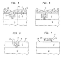
- FIG. 4 shows conductive film 31 formed over top surface 26 of titanium-tantalum barrier layer film 25.
- titanium-tantalum barrier layer film 25 may represent either of barrier layer film 125 as shown in FIG. 1, or barrier layer film 225 as shown in FIG. 3.
- Conductive film 31 may be formed by sputter deposition, CVD, PVD, electrodeposition, electroplating or electro-less plating processes.
- conductive layer film 31 may be copper, but in alternative embodiments it may be nickel or aluminum.
- Thickness 32 of conductive film 31 may be any suitable thickness chosen to ensure that conductive film 31 completely fills opening 21. By filling opening 21, it is meant that conductive film 31 fully occupies the portion of opening below the plane formed by upper surface 19 of dielectric film 17.
- conductive film 31 may be formed by electrodeposition.
- a seed layer film 33 is also formed between titanium-tantalum barrier layer film 25 and conductive film 31.
- seed layer film 33 may be formed of copper.
- Seed layer film 33 may be formed using conventional CVD or PVD methods as available in the art, or it may be formed using electroless plating processes. It can be also seen that seed layer film 33 is formed over top surface 26 of titanium-tantalum barrier layer film 25 and does not completely fill opening 21. As in the embodiment shown in FIG. 4, conductive film 31 which is formed by electrodeposition onto seed layer film 33, completely fills opening 21.
- FIG. 6 a cross-sectional view of an interconnect structure, or conductive wire 35, is shown. It can be seen that portions of titanium-tantalum barrier layer film 25 and conductive film 31 which lie above the plane formed by upper surface 19 of dielectric film 17, have been removed.
- a polishing operation such as chemical mechanical polishing (CMP) may be used to remove the films and planarize the surface as shown.
- upper surface 37 of conductive wire 35 is substantially co-planar with upper surface 19 of dielectric film 17.
- conductive film 31 is bounded on the sides and the bottom by titanium-tantalum barrier layer film 25.
- copper is the preferred conductive material 31, although nickel and aluminum may be used alternatively.
- FIG. 5, which additionally includes seed layer film 33 may be similarly planarized.
- FIG. 7 shows another exemplary embodiment of a film structure including a barrier layer film formed according to the present invention.
- the conductive film is formed over a surface of a dielectric material according to non-damascene techniques. This portion of a film formed over a top surface of a substrate may be as shown in region 40 of FIG. 4, for example.
- titanium-tantalum barrier layer film 25 may, again, represent barrier layer film 125, shown and described in conjunction FIG. 1, or barrier layer film 225 shown and described in conjunction with FIG. 3. Titanium-tantalum barrier layer film 25 is formed over surface 19 of dielectric film 17.
- Conductive film 31, shown and described in conjunction with FIG. 4, is formed over top surface 26 of titanium-tantalum barrier layer film 25.
- the present invention is shown and described in conjunction with aluminum, nickel, and copper conductive films, it should be understood that the invention is not intended to be limited to the embodiments shown and described. Rather, the titanium-tantalum barrier layer film including a lower portion being titanium rich/tantalum deficient and an upper section being titanium deficient/tantalum rich, may be used in any application where such a film is suitable.
- the barrier layer film may be formed over various other features. The barrier layer film and the structures formed using the barrier layer film, may be utilized within various semiconductor devices, and may be formed over the various substrates used in the semiconductor manufacturing industry.
- the process for forming the barrier layer film according to the present invention is also not intended to be limited to the formation processes described above. Rather, various other processing techniques may be used to produce the titanium-tantalum barrier layer film. In addition, various other processing operations may be combined to utilize the advantages provided by the described embodiments of the titanium-tantalum barrier layer film.
- the non-damascene patterned conductive wire shown in FIG. 7 may additionally include a seed layer film formed between the titanium-tantalum barrier layer film and the conductive film, in the exemplary embodiment wherein the conductive layer film is formed by electroplating techniques.
Landscapes
- Internal Circuitry In Semiconductor Integrated Circuit Devices (AREA)
- Electrodes Of Semiconductors (AREA)
Abstract
Description
Claims (45)
- A process for depositing a film onto a substrate, comprising the steps of:a) providing a substrate having a substrate surface;b) depositing a titanium-tantalum film over the substrate surface, the film having a gradient of titanium concentration therewithin, the titanium concentration being maximized at a section of the film nearest the substrate surface, and decreasing along a direction extending perpendicularly away from the substrate surface.
- The process as in claim 1, in which step b) includes providing a sputtering target within a sputtering apparatus, the sputtering target being formed of a homogenous composition including titanium and tantalum.
- The process as in claim 2, wherein step b) comprises supplying a current to the sputtering target, thereby continuously sputtering the titanium-tantalum film by:i. sputtering a lower section of the titanium-tantalum film over the substrate surface, the lower section having a first titanium weight percentage;ii. sputtering a central section of the titanium-tantalum film onto the lower section, the central section having a second titanium weight percentage being less than the first titanium weight percentage; andiii. sputtering an upper section of the titanium-tantalum film onto the central section, the upper section having a third titanium weight percentage being less than the second titanium weight percentage.
- The process as in claim 1, in which step b) includes providing a titanium sputtering target within a sputtering apparatus and a tantalum sputtering target within the sputtering apparatus, each sputtering target being separately controllable and adapted for sputtering material onto the substrate surface.
- The process as in claim 4, in which step b) includes supplying a current to the titanium sputtering target and supplying a further current to the tantalum sputtering target, thereby continuously sputtering the titanium-tantalum film by:i. sputtering a lower section of the titanium-tantalum film over the substrate surface, the lower section having a first titanium weight percentage;ii. sputtering a central section of the titanium-tantalum film onto the lower section, the central section having a second titanium weight percentage being less than the first titanium weight percentage; andiii. sputtering an upper section of the titanium-tantalum film onto the central section, the upper section having a third titanium weight percentage being less than the second titanium weight percentage.
- The process as in claim 5, further comprising varying at least one of the amperage of each of the current and the further current; a voltage level of each of the titanium sputtering target and the tantalum sputtering target; and, a power level of each of the titanium sputtering target and the tantalum sputtering target, during step b).
- The process as in claim 1, wherein step b) comprises chemical vapor deposition.
- The process as in claim 1, wherein step b) comprises physical vapor deposition.
- A process for forming a semiconductor device comprising:a) providing a semiconductor substrate having a dielectric film formed thereon, the dielectric film including a dielectric surface and having an opening formed therein, the opening including sidewalls and a bottom;b) depositing a titanium-tantalum barrier layer on the dielectric surface and on the sidewalls and the bottom but not filling the opening;c) depositing a conductive film over the barrier layer and filing the opening; andd) removing portions of the barrier layer and the conductive film from over a plane formed by the dielectric surface, wherein other portions of the barrier layer and the conductive film remain within the opening.
- The process as in claim 9, in which step a) includes forming the dielectric film by one of CVD and spin-on techniques.
- The process as in claim 9, wherein the opening is a dual-damascene trench structure, and step d) comprises chemical mechanical polishing.
- The process as in claim 9, wherein step b) comprises forming a titanium film, then forming a tantalum film over the titanium film.
- The process as in claim 12, wherein each of the titanium film and the tantalum film include a thickness within a range of 5 nanometers to 100 nanometers.
- The process as in claim 12, wherein step b) comprises forming each of the titanium film and the tantalum film using one of chemical vapor deposition and physical vapor deposition.
- The process as in claim 12, wherein step b) comprises forming at least one of the titanium film and the tantalum film using Metallo-Organic chemical vapor deposition.
- The process as in claim 9, wherein the titanium-tantalum barrier layer has a gradient of titanium concentration therewithin, the titanium concentration being maximized at a section of the barrier layer nearest to an interface formed between the titanium-tantalum barrier layer and the dielectric film, and decreasing along a direction extending perpendicularly away from the interface, and step b) comprises depositing the titanium-tantalum barrier layer using one of chemical vapor deposition and physical vapor deposition.
- The process as in claim 9, wherein step b) comprises the steps of:wherein the titanium-tantalum barrier layer has a gradient of titanium concentration therewithin, the titanium concentration being maximized at a section of the barrier layer nearest an interface formed between the titanium-tantalum barrier layer and the dielectric film, and decreasing along a direction extending perpendicularly away from the interface.i) providing a sputtering target within a sputtering apparatus, the sputtering target being formed of a homogenous composition including titanium and tantalum;ii) positioning the semiconductor substrate within the sputtering apparatus; andiii) supplying a current to the sputtering target, thereby sputtering a titanium-tantalum film, the titanium-tantalum film forming the titanium-tantalum barrier layer, and
- The process as in claim 9, wherein step b) comprises the steps of:wherein the titanium-tantalum barrier layer has a gradient of titanium concentration therewithin, the titanium concentration being maximized at a section of the barrier layer nearest an interface formed between the titanium-tantalum barrier layer and the dielectric film, and decreasing along a direction extending perpendicularly away from the interface.i) positioning the semiconductor substrate within a sputtering apparatus;ii) providing a titanium sputtering target within the sputtering apparatus and a tantalum sputtering target within the sputtering apparatus, each sputtering target adapted to sputter material onto the semiconductor substrate; andiii) supplying a current to the titanium sputtering target and supplying a further current to the tantalum sputtering target, thereby sputtering a titanium-tantalum film, the titanium-tantalum film forming the titanium-tantalum barrier layer, and
- The process as in claim 17, wherein step b) further comprises the step iv) of heating the titanium-tantalum barrier layer.
- The process as in claim 17, wherein step iii) comprises supplying a current to the sputtering target, thereby continuously sputtering the titanium-tantalum film by:A. sputtering a lower section of the titanium-tantalum film onto the dielectric surface, the sidewalls, and the bottom, the lower section having a first titanium weight percentage;B. sputtering a central section of the titanium-tantalum film onto the lower section, the central section having a second titanium weight percentage being less than the first titanium weight percentage; andC. sputtering an upper section of the titanium-tantalum film onto the central section, the upper section having a third titanium weight percentage being less than the second titanium weight percentage.
- The process as in claim 9, wherein step c) comprises depositing one of a nickel film and an aluminum film.
- The process as in claim 9, wherein step c) comprises depositing a copper film.
- The process as in claim 9, further comprising step bl) forming an electroplating seed layer over the titanium-tantalum barrier layer but not filing the opening therewith and wherein step c) comprises forming a copper film by electrodeposition.
- A process for forming a semiconductor device, comprising the steps of:a) providing a semiconductor substrate having a dielectric film formed thereon;b) depositing a titanium-tantalum barrier layer over a dielectric surface of the dielectric film;c) depositing a conductive film of one of nickel and aluminum over the titanium-tantalum barrier layer thereby forming a composite film of the titanium-tantalum barrier layer and the conductive film; andd) removing portions of the composite film thereby patterning the composite film and forming an interconnect pattern thereof.
- The process as in claim 24, further comprising step bl) forming an electroplating seed layer over the titanium-tantalum barrier layer, and wherein step c) comprises electroplating, and the composite film further includes the electroplating seed layer.
- The process as in claim 24, wherein step b) comprises forming a titanium film then forming a tantalum film over the titanium film.
- The process as in claim 24, wherein step b) comprises the steps of:wherein the titanium-tantalum barrier layer has a gradient of titanium concentration therewithin, the titanium concentration decreasing along a direction extending perpendicularly away from the dielectric surface.i) providing a sputtering target within a sputtering apparatus, the sputtering target being formed of a homogenous composition including titanium and tantalum;ii) positioning the semiconductor substrate within the sputtering apparatus; andiii) supplying a current to the sputtering target thereby sputtering a titanium-tantalum film over the dielectric surface, the titanium-tantalum film forming the titanium-tantalum barrier layer, and
- A titanium-tantalum film formed according to the process as in claim 3.
- A semiconductor device comprising a dielectric layer having an opening formed therein, an exposed surface including a top surface of the dielectric layer and sidewalls and a bottom portion of the opening, and a titanium-tantalum barrier layer formed over the exposed surface.
- The semiconductor device as in claim 29, further comprising a conductive film formed over the barrier layer.
- The semiconductor device as in claim 30, wherein the conductive film comprises copper.
- The semiconductor device as in claim 30, further comprising a seed layer film interposed between the titanium-tantalum barrier layer and the conductive film.
- The semiconductor device as in claim 30, wherein the conductive film comprises one of nickel and aluminum.
- The semiconductor device as in claim 29, wherein the titanium-tantalum barrier layer comprises a tantalum film having a thickness within a range of 5-100 nanometers, formed over a titanium film having a thickness within a range of 5-100 nanometers.
- The semiconductor device as in claim 29, wherein the titanium-tantalum barrier layer comprises a film having a gradient of titanium concentration therewithin, the titanium concentration decreasing along a direction extending perpendicularly away from the exposed surface.
- The semiconductor device as in claim 35, wherein the titanium concentration is maximized at or near the exposed surface.
- The semiconductor device as in claim 29, wherein the titanium-tantalum barrier layer comprises a film having a gradient of tantalum concentration therewithin, the tantalum concentration increasing along a direction extending perpendicularly away from the exposed surface.
- The semiconductor device as in claim 37, wherein the tantalum concentration is minimized at or near the exposed surface.
- A semiconductor device as in claim 29, wherein the titanium-tantalum barrier layer comprises a film being relatively titanium-rich adjacent the exposed surface and relatively titanium-deficient adjacent an upper surface of the film.
- A damascene structure formed within a damascene opening formed within a dielectric film, the dielectric film having a top surface, the damascene opening including sidewalls and a bottom surface, the damascene structure comprising a titanium-tantalum barrier layer formed on the sidewalls and the bottom surface but not filling the opening, a conductive layer formed over the barrier layer and filing the opening, the damascene structure including an upper surface being essentially planar with the top surface.
- The damascene structure as in claim 40, wherein the titanium-tantalum barrier layer includes a leading surface forming an interface with the sidewalls and the bottom surface, and a gradient of titanium concentration therewithin, the titanium concentration being maximized at or near the interface and decreasing along a direction extending perpendicularly away from the interface.
- The damascene structure as in claim 40, wherein the titanium-tantalum barrier layer is a composite film including a titanium film formed on the sidewalls and the bottom surface, and a tantalum film formed over the titanium film, the conductive layer being formed over the tantalum film.
- The damascene structure as in claim 40, further comprising a seed layer film interposed between the titanium-tantalum barrier layer and the conductive layer.
- The damascene structure as in claim 40, wherein the conductive layer comprises copper.
- The damascene structure as in claim 40, wherein the conductive layer comprises one of nickel and aluminum.
Applications Claiming Priority (4)
| Application Number | Priority Date | Filing Date | Title |
|---|---|---|---|
| US519193 | 1990-05-04 | ||
| US13556599P | 1999-05-24 | 1999-05-24 | |
| US135565P | 1999-05-24 | ||
| US09/519,193 US6331484B1 (en) | 1999-03-29 | 2000-03-06 | Titanium-tantalum barrier layer film and method for forming the same |
Publications (2)
| Publication Number | Publication Date |
|---|---|
| EP1063687A2 true EP1063687A2 (en) | 2000-12-27 |
| EP1063687A3 EP1063687A3 (en) | 2003-03-19 |
Family
ID=26833449
Family Applications (1)
| Application Number | Title | Priority Date | Filing Date |
|---|---|---|---|
| EP00304061A Withdrawn EP1063687A3 (en) | 1999-05-24 | 2000-05-15 | Titanium-tantalum barrier layer film and method for forming the same |
Country Status (2)
| Country | Link |
|---|---|
| US (1) | US6331484B1 (en) |
| EP (1) | EP1063687A3 (en) |
Cited By (8)
| Publication number | Priority date | Publication date | Assignee | Title |
|---|---|---|---|---|
| US6933225B2 (en) | 2000-03-07 | 2005-08-23 | Asm International N.V. | Graded thin films |
| US6955986B2 (en) * | 2003-03-27 | 2005-10-18 | Asm International N.V. | Atomic layer deposition methods for forming a multi-layer adhesion-barrier layer for integrated circuits |
| US7419903B2 (en) | 2000-03-07 | 2008-09-02 | Asm International N.V. | Thin films |
| US7498242B2 (en) | 2005-02-22 | 2009-03-03 | Asm America, Inc. | Plasma pre-treating surfaces for atomic layer deposition |
| US7563715B2 (en) | 2005-12-05 | 2009-07-21 | Asm International N.V. | Method of producing thin films |
| US7972977B2 (en) | 2006-10-05 | 2011-07-05 | Asm America, Inc. | ALD of metal silicate films |
| US9139906B2 (en) | 2001-03-06 | 2015-09-22 | Asm America, Inc. | Doping with ALD technology |
| US20240011840A1 (en) * | 2021-03-24 | 2024-01-11 | Panasonic Intellectual Property Management Co., Ltd. | Multilayer body, electronic device, and method of producing multilayer body |
Families Citing this family (13)
| Publication number | Priority date | Publication date | Assignee | Title |
|---|---|---|---|---|
| US6368954B1 (en) * | 2000-07-28 | 2002-04-09 | Advanced Micro Devices, Inc. | Method of copper interconnect formation using atomic layer copper deposition |
| US6498397B1 (en) * | 2000-11-06 | 2002-12-24 | Advanced Micro Devices, Inc. | Seed layer with annealed region for integrated circuit interconnects |
| US6504251B1 (en) * | 2000-11-18 | 2003-01-07 | Advanced Micro Devices, Inc. | Heat/cold amorphized barrier layer for integrated circuit interconnects |
| US20040065955A1 (en) * | 2002-09-24 | 2004-04-08 | Kim Hyunchul C. | Apparatus and method of using thin film material as diffusion barrier for metallization |
| US6875693B1 (en) * | 2003-03-26 | 2005-04-05 | Lsi Logic Corporation | Via and metal line interface capable of reducing the incidence of electro-migration induced voids |
| US8791018B2 (en) * | 2006-12-19 | 2014-07-29 | Spansion Llc | Method of depositing copper using physical vapor deposition |
| JP4324617B2 (en) * | 2007-02-26 | 2009-09-02 | 東京エレクトロン株式会社 | Sputter deposition method and sputter deposition apparatus |
| US8679301B2 (en) * | 2007-08-01 | 2014-03-25 | HGST Netherlands B.V. | Repeatability for RF MgO TMR barrier layer process by implementing Ti pasting |
| US7919409B2 (en) | 2008-08-15 | 2011-04-05 | Air Products And Chemicals, Inc. | Materials for adhesion enhancement of copper film on diffusion barriers |
| JP2010123586A (en) * | 2008-11-17 | 2010-06-03 | Nec Electronics Corp | Semiconductor device, and method of manufacturing the same |
| US20140264865A1 (en) * | 2013-03-14 | 2014-09-18 | Infineon Technologies Ag | Semiconductor device and manufacturing method thereof |
| US11837449B2 (en) | 2016-03-25 | 2023-12-05 | Jx Metals Corporation | Ti-Nb alloy sputtering target and production method thereof |
| US11318435B2 (en) * | 2018-09-21 | 2022-05-03 | California Institute Of Technology | 3D printing of metal containing structures |
Family Cites Families (6)
| Publication number | Priority date | Publication date | Assignee | Title |
|---|---|---|---|---|
| US5891513A (en) * | 1996-01-16 | 1999-04-06 | Cornell Research Foundation | Electroless CU deposition on a barrier layer by CU contact displacement for ULSI applications |
| US5770517A (en) * | 1997-03-21 | 1998-06-23 | Advanced Micro Devices, Inc. | Semiconductor fabrication employing copper plug formation within a contact area |
| US5930669A (en) * | 1997-04-03 | 1999-07-27 | International Business Machines Corporation | Continuous highly conductive metal wiring structures and method for fabricating the same |
| US6069068A (en) * | 1997-05-30 | 2000-05-30 | International Business Machines Corporation | Sub-quarter-micron copper interconnections with improved electromigration resistance and reduced defect sensitivity |
| US5882738A (en) * | 1997-12-19 | 1999-03-16 | Advanced Micro Devices, Inc. | Apparatus and method to improve electromigration performance by use of amorphous barrier layer |
| US6054398A (en) * | 1999-05-14 | 2000-04-25 | Advanced Micro Devices, Inc. | Semiconductor interconnect barrier for fluorinated dielectrics |
-
2000
- 2000-03-06 US US09/519,193 patent/US6331484B1/en not_active Expired - Lifetime
- 2000-05-15 EP EP00304061A patent/EP1063687A3/en not_active Withdrawn
Cited By (11)
| Publication number | Priority date | Publication date | Assignee | Title |
|---|---|---|---|---|
| US6933225B2 (en) | 2000-03-07 | 2005-08-23 | Asm International N.V. | Graded thin films |
| US7419903B2 (en) | 2000-03-07 | 2008-09-02 | Asm International N.V. | Thin films |
| US7981791B2 (en) | 2000-03-07 | 2011-07-19 | Asm International N.V. | Thin films |
| US20110256718A1 (en) * | 2000-03-07 | 2011-10-20 | Asm International N.V. | Thin films |
| US9139906B2 (en) | 2001-03-06 | 2015-09-22 | Asm America, Inc. | Doping with ALD technology |
| US6955986B2 (en) * | 2003-03-27 | 2005-10-18 | Asm International N.V. | Atomic layer deposition methods for forming a multi-layer adhesion-barrier layer for integrated circuits |
| US7498242B2 (en) | 2005-02-22 | 2009-03-03 | Asm America, Inc. | Plasma pre-treating surfaces for atomic layer deposition |
| US7563715B2 (en) | 2005-12-05 | 2009-07-21 | Asm International N.V. | Method of producing thin films |
| US7972977B2 (en) | 2006-10-05 | 2011-07-05 | Asm America, Inc. | ALD of metal silicate films |
| US8563444B2 (en) | 2006-10-05 | 2013-10-22 | Asm America, Inc. | ALD of metal silicate films |
| US20240011840A1 (en) * | 2021-03-24 | 2024-01-11 | Panasonic Intellectual Property Management Co., Ltd. | Multilayer body, electronic device, and method of producing multilayer body |
Also Published As
| Publication number | Publication date |
|---|---|
| US6331484B1 (en) | 2001-12-18 |
| EP1063687A3 (en) | 2003-03-19 |
Similar Documents
| Publication | Publication Date | Title |
|---|---|---|
| US6331484B1 (en) | Titanium-tantalum barrier layer film and method for forming the same | |
| CN1081390C (en) | Refractory metal capped low resistivity metal conductor lines and vias formed using PVD and CVD | |
| US7105434B2 (en) | Advanced seed layery for metallic interconnects | |
| US7417321B2 (en) | Via structure and process for forming the same | |
| KR100506139B1 (en) | Dual damascene metallization | |
| US6924226B2 (en) | Methods for making multiple seed layers for metallic interconnects | |
| US6566258B1 (en) | Bi-layer etch stop for inter-level via | |
| JP2999991B2 (en) | Manufacturing method of continuous high conductivity metal wiring | |
| US20090239372A1 (en) | Seed Layers for Electroplated Interconnects | |
| US6486560B1 (en) | Semiconductor device fabricated by a method of reducing electromigration in copper lines by forming an interim layer of calcium-doped copper seed layer in a chemical solution | |
| JP2002033323A (en) | Method of manufacturing semiconductor device having copper interconnect | |
| US20080156636A1 (en) | Homogeneous Copper Interconnects for BEOL | |
| JP4005295B2 (en) | Manufacturing method of semiconductor device | |
| US20040259348A1 (en) | Method of reducing post-CMP defectivity | |
| JP3445557B2 (en) | Titanium-tantalum barrier layer thin film and method of forming the same | |
| JP2000357669A (en) | Method for filling substrate surface features with copper | |
| JP2000208517A (en) | Method for manufacturing semiconductor device | |
| JP3269490B2 (en) | Semiconductor integrated circuit device and method of manufacturing the same | |
| JP2003124216A (en) | Wiring seed film and wiring method for semiconductor device | |
| JP2002141303A (en) | In situ co-deposition of Si in diffusion barrier materials with improved wettability, barrier efficiency and device reliability | |
| JP2003332339A (en) | Method and apparatus for improving adhesion between layers in an integrated device | |
| KR20040006116A (en) | Method for forming Cu interconnect | |
| KR20030027844A (en) | Structure and method for reducing electromigration |
Legal Events
| Date | Code | Title | Description |
|---|---|---|---|
| PUAI | Public reference made under article 153(3) epc to a published international application that has entered the european phase |
Free format text: ORIGINAL CODE: 0009012 |
|
| AK | Designated contracting states |
Kind code of ref document: A2 Designated state(s): AT BE CH CY DE DK ES FI FR GB GR IE IT LI LU MC NL PT SE |
|
| AX | Request for extension of the european patent |
Free format text: AL;LT;LV;MK;RO;SI |
|
| PUAL | Search report despatched |
Free format text: ORIGINAL CODE: 0009013 |
|
| AK | Designated contracting states |
Kind code of ref document: A3 Designated state(s): AT BE CH CY DE DK ES FI FR GB GR IE IT LI LU MC NL PT SE Designated state(s): AT BE CH CY DE DK ES FI FR GB GR IE IT LI LU MC NL PT SE |
|
| AX | Request for extension of the european patent |
Extension state: AL LT LV MK RO SI |
|
| AKX | Designation fees paid | ||
| REG | Reference to a national code |
Ref country code: DE Ref legal event code: 8566 |
|
| STAA | Information on the status of an ep patent application or granted ep patent |
Free format text: STATUS: THE APPLICATION IS DEEMED TO BE WITHDRAWN |
|
| 18D | Application deemed to be withdrawn |
Effective date: 20030920 |