EP1059702A2 - Ground terminal - Google Patents
Ground terminal Download PDFInfo
- Publication number
- EP1059702A2 EP1059702A2 EP00304317A EP00304317A EP1059702A2 EP 1059702 A2 EP1059702 A2 EP 1059702A2 EP 00304317 A EP00304317 A EP 00304317A EP 00304317 A EP00304317 A EP 00304317A EP 1059702 A2 EP1059702 A2 EP 1059702A2
- Authority
- EP
- European Patent Office
- Prior art keywords
- ground terminal
- board
- spring contact
- board portion
- integrally
- Prior art date
- Legal status (The legal status is an assumption and is not a legal conclusion. Google has not performed a legal analysis and makes no representation as to the accuracy of the status listed.)
- Granted
Links
Images

Classifications
-
- H—ELECTRICITY
- H01—ELECTRIC ELEMENTS
- H01R—ELECTRICALLY-CONDUCTIVE CONNECTIONS; STRUCTURAL ASSOCIATIONS OF A PLURALITY OF MUTUALLY-INSULATED ELECTRICAL CONNECTING ELEMENTS; COUPLING DEVICES; CURRENT COLLECTORS
- H01R12/00—Structural associations of a plurality of mutually-insulated electrical connecting elements, specially adapted for printed circuits, e.g. printed circuit boards [PCB], flat or ribbon cables, or like generally planar structures, e.g. terminal strips, terminal blocks; Coupling devices specially adapted for printed circuits, flat or ribbon cables, or like generally planar structures; Terminals specially adapted for contact with, or insertion into, printed circuits, flat or ribbon cables, or like generally planar structures
- H01R12/50—Fixed connections
- H01R12/51—Fixed connections for rigid printed circuits or like structures
- H01R12/52—Fixed connections for rigid printed circuits or like structures connecting to other rigid printed circuits or like structures
-
- H—ELECTRICITY
- H01—ELECTRIC ELEMENTS
- H01R—ELECTRICALLY-CONDUCTIVE CONNECTIONS; STRUCTURAL ASSOCIATIONS OF A PLURALITY OF MUTUALLY-INSULATED ELECTRICAL CONNECTING ELEMENTS; COUPLING DEVICES; CURRENT COLLECTORS
- H01R12/00—Structural associations of a plurality of mutually-insulated electrical connecting elements, specially adapted for printed circuits, e.g. printed circuit boards [PCB], flat or ribbon cables, or like generally planar structures, e.g. terminal strips, terminal blocks; Coupling devices specially adapted for printed circuits, flat or ribbon cables, or like generally planar structures; Terminals specially adapted for contact with, or insertion into, printed circuits, flat or ribbon cables, or like generally planar structures
- H01R12/70—Coupling devices
- H01R12/7076—Coupling devices for connection between PCB and component, e.g. display
-
- H—ELECTRICITY
- H01—ELECTRIC ELEMENTS
- H01R—ELECTRICALLY-CONDUCTIVE CONNECTIONS; STRUCTURAL ASSOCIATIONS OF A PLURALITY OF MUTUALLY-INSULATED ELECTRICAL CONNECTING ELEMENTS; COUPLING DEVICES; CURRENT COLLECTORS
- H01R13/00—Details of coupling devices of the kinds covered by groups H01R12/70 or H01R24/00 - H01R33/00
- H01R13/02—Contact members
- H01R13/22—Contacts for co-operating by abutting
- H01R13/24—Contacts for co-operating by abutting resilient; resiliently-mounted
- H01R13/2442—Contacts for co-operating by abutting resilient; resiliently-mounted with a single cantilevered beam
-
- H—ELECTRICITY
- H01—ELECTRIC ELEMENTS
- H01R—ELECTRICALLY-CONDUCTIVE CONNECTIONS; STRUCTURAL ASSOCIATIONS OF A PLURALITY OF MUTUALLY-INSULATED ELECTRICAL CONNECTING ELEMENTS; COUPLING DEVICES; CURRENT COLLECTORS
- H01R13/00—Details of coupling devices of the kinds covered by groups H01R12/70 or H01R24/00 - H01R33/00
- H01R13/648—Protective earth or shield arrangements on coupling devices, e.g. anti-static shielding
- H01R13/658—High frequency shielding arrangements, e.g. against EMI [Electro-Magnetic Interference] or EMP [Electro-Magnetic Pulse]
- H01R13/6581—Shield structure
- H01R13/6582—Shield structure with resilient means for engaging mating connector
-
- H—ELECTRICITY
- H01—ELECTRIC ELEMENTS
- H01R—ELECTRICALLY-CONDUCTIVE CONNECTIONS; STRUCTURAL ASSOCIATIONS OF A PLURALITY OF MUTUALLY-INSULATED ELECTRICAL CONNECTING ELEMENTS; COUPLING DEVICES; CURRENT COLLECTORS
- H01R13/00—Details of coupling devices of the kinds covered by groups H01R12/70 or H01R24/00 - H01R33/00
- H01R13/648—Protective earth or shield arrangements on coupling devices, e.g. anti-static shielding
- H01R13/658—High frequency shielding arrangements, e.g. against EMI [Electro-Magnetic Interference] or EMP [Electro-Magnetic Pulse]
- H01R13/6591—Specific features or arrangements of connection of shield to conductive members
- H01R13/6594—Specific features or arrangements of connection of shield to conductive members the shield being mounted on a PCB and connected to conductive members
-
- H—ELECTRICITY
- H05—ELECTRIC TECHNIQUES NOT OTHERWISE PROVIDED FOR
- H05K—PRINTED CIRCUITS; CASINGS OR CONSTRUCTIONAL DETAILS OF ELECTRIC APPARATUS; MANUFACTURE OF ASSEMBLAGES OF ELECTRICAL COMPONENTS
- H05K1/00—Printed circuits
- H05K1/02—Details
- H05K1/0213—Electrical arrangements not otherwise provided for
- H05K1/0215—Grounding of printed circuits by connection to external grounding means
-
- H—ELECTRICITY
- H01—ELECTRIC ELEMENTS
- H01R—ELECTRICALLY-CONDUCTIVE CONNECTIONS; STRUCTURAL ASSOCIATIONS OF A PLURALITY OF MUTUALLY-INSULATED ELECTRICAL CONNECTING ELEMENTS; COUPLING DEVICES; CURRENT COLLECTORS
- H01R12/00—Structural associations of a plurality of mutually-insulated electrical connecting elements, specially adapted for printed circuits, e.g. printed circuit boards [PCB], flat or ribbon cables, or like generally planar structures, e.g. terminal strips, terminal blocks; Coupling devices specially adapted for printed circuits, flat or ribbon cables, or like generally planar structures; Terminals specially adapted for contact with, or insertion into, printed circuits, flat or ribbon cables, or like generally planar structures
- H01R12/50—Fixed connections
- H01R12/51—Fixed connections for rigid printed circuits or like structures
- H01R12/55—Fixed connections for rigid printed circuits or like structures characterised by the terminals
- H01R12/57—Fixed connections for rigid printed circuits or like structures characterised by the terminals surface mounting terminals
-
- H—ELECTRICITY
- H01—ELECTRIC ELEMENTS
- H01R—ELECTRICALLY-CONDUCTIVE CONNECTIONS; STRUCTURAL ASSOCIATIONS OF A PLURALITY OF MUTUALLY-INSULATED ELECTRICAL CONNECTING ELEMENTS; COUPLING DEVICES; CURRENT COLLECTORS
- H01R2101/00—One pole
-
- H—ELECTRICITY
- H05—ELECTRIC TECHNIQUES NOT OTHERWISE PROVIDED FOR
- H05K—PRINTED CIRCUITS; CASINGS OR CONSTRUCTIONAL DETAILS OF ELECTRIC APPARATUS; MANUFACTURE OF ASSEMBLAGES OF ELECTRICAL COMPONENTS
- H05K2201/00—Indexing scheme relating to printed circuits covered by H05K1/00
- H05K2201/10—Details of components or other objects attached to or integrated in a printed circuit board
- H05K2201/10227—Other objects, e.g. metallic pieces
- H05K2201/10265—Metallic coils or springs, e.g. as part of a connection element
-
- H—ELECTRICITY
- H05—ELECTRIC TECHNIQUES NOT OTHERWISE PROVIDED FOR
- H05K—PRINTED CIRCUITS; CASINGS OR CONSTRUCTIONAL DETAILS OF ELECTRIC APPARATUS; MANUFACTURE OF ASSEMBLAGES OF ELECTRICAL COMPONENTS
- H05K2201/00—Indexing scheme relating to printed circuits covered by H05K1/00
- H05K2201/10—Details of components or other objects attached to or integrated in a printed circuit board
- H05K2201/10227—Other objects, e.g. metallic pieces
- H05K2201/1031—Surface mounted metallic connector elements
-
- Y—GENERAL TAGGING OF NEW TECHNOLOGICAL DEVELOPMENTS; GENERAL TAGGING OF CROSS-SECTIONAL TECHNOLOGIES SPANNING OVER SEVERAL SECTIONS OF THE IPC; TECHNICAL SUBJECTS COVERED BY FORMER USPC CROSS-REFERENCE ART COLLECTIONS [XRACs] AND DIGESTS
- Y02—TECHNOLOGIES OR APPLICATIONS FOR MITIGATION OR ADAPTATION AGAINST CLIMATE CHANGE
- Y02P—CLIMATE CHANGE MITIGATION TECHNOLOGIES IN THE PRODUCTION OR PROCESSING OF GOODS
- Y02P70/00—Climate change mitigation technologies in the production process for final industrial or consumer products
- Y02P70/50—Manufacturing or production processes characterised by the final manufactured product
Definitions
- the present device relates generally to a ground terminal useful for grounding a printed circuit board to a shielding plate or a chassis in order to prevent electromagnetic induction interference and high frequency induction interference.
- Devices for grounding a printed circuit board to a shield component. These devices typically include a ground terminal 20', for example, as shown in Figure 6A, which comprises a board portion 1' to be mounted to a ground pattern on a printed circuit board 10' and a spring contact 2' projecting integrally and opposite to the direction of the board portion from one side of the board portion.
- a ground terminal 20' for example, as shown in Figure 6A, which comprises a board portion 1' to be mounted to a ground pattern on a printed circuit board 10' and a spring contact 2' projecting integrally and opposite to the direction of the board portion from one side of the board portion.
- the device of the present invention provides a ground terminal comprising, a board portion to be mounted to a ground pattern on a printed circuit board, and a spring contact projecting integrally and opposite to the direction of the board portion from one side of the board portion, and the ground terminal is further provided with an engaging wall which stands up integrally from said board portion to engage the end portion of said spring contact.
- the engaging wall operates as a stop against irregular external forces applied by the touch of fingers or the like on the terminal to protect the terminal from deformation.
- Figures 1 through 5 show the preferred embodiments in accordance with the device of the present invention.
- the ground terminal 20 of the device of the present invention comprises a board portion 1 and a spring contact 2.
- the board portion 1 may be mounted on a ground pattern (not shown) on a printed circuit board by soldering or other mounting technique.
- the spring contact 2 projects integrally from and opposite to the direction of the board portion 1 from one side of the board portion. It is contemplated that the underside of the board portion 1 is preferably plated for improved solderability.
- the spring contact comprises an end portion 2a, a first body portion 2b which is configured by being integrally connected to the end portion and extends therefrom such that the first body portion 2b is opposed to the board portion 1, and a second body portion 2c which couples the first body portion with the board portion.
- the ground terminal 20 is further provided with an engaging wall 3 which stands up integrally from said board portion 1 and engages the end portion 2a of said spring contact.
- the engaging wall 3 specifically operates as a stop wherein the end of the engaging wall 3 holds the end portion 2a of the spring contact.
- the engaging walls comprise side walls 3a standing up integrally from the opposite sides of said board portion and upper walls 3b extending integrally from the side walls such that the upper walls are opposed to each other, and thus engage the both side of the end portion of the spring contact.
- the board portion is soldered to a ground pattern on a printed circuit board.
- the board portion is provided with through holes 11 such that the soldered joint can be reliable in its strength and in its position accuracy.
- FIG. 5A and 5B shows the ground terminal 20 according to the embodiment of the present invention, which is placed on printed circuit board 10.
- the board portion 1 of the ground terminal 20 is secured to a ground pattern on a printed circuit board by soldering. More specifically, a plurality of the ground terminals 20 are placed on a table.
- An automatic machine (not shown) absorbs the first body portion of a spring contact by using vacuum and at the same time carries it to a predetermined position in the printed circuit board, and there, by releasing the vacuum absorption, the terminal is placed with the underside thereof down on the circuit board. Then, by passing the circuit board through a soldering bath, the terminal is soldered onto the primed circuit board as well as other circuit elements on the printed circuit board.
- the ground terminal 20 is brought into contact with the shielding panel, chassis, frame or the like in order to ground the ground pattern on the printed circuit board thereto.
- This work is performed by housing the circuit board via the ground terminal of the device into a casing that is provided, for example, with a shielding panel inside thereof.
- the spring contact is pressed down toward the side of the board portion (inside), so that the end portion of the spring contact may be separated from the engaging wall. This condition can keep the ground terminal in enough contact with the shielding panel.
- the part of the spring contact to contact the shielding panel is required to be, even under contact with the shielding panel, higher than the end of the engaging wall, as well as under non-contact condition. Therefore, there is a permissible range within the movable step (oscillation range ) of the spring contact.
- the ground terminal according to the device of the present invention is provided with an engaging wall that stands up integrally from the board portion to engage the end portion of the spring contact.
- the engaging wall operates as a stopper against irregular external forces applied when a finger or the like touches the ground terminal, to protect the terminal from deformation. Therefore, the ground terminal according to the present device can eliminate disadvantages such as poor contact made between deformed spring contacts and chassis, and obstacles to housing operations caused by the deformed spring contacts hitched on chassis when boards are housed in chassis.
- ground terminal of the present. device can be mounted on the circuit board, automatic machines can be used. Accordingly, it is possible to reduce the number of operation processes without any person.
- the use of the ground terminal of the device provides many advantages and so is useful for taking measures against noise and EMI in various electronics equipment, such as displays using CRT, TFT and STN color liquid crystal.
Landscapes
- Engineering & Computer Science (AREA)
- Microelectronics & Electronic Packaging (AREA)
- Coupling Device And Connection With Printed Circuit (AREA)
- Multi-Conductor Connections (AREA)
Abstract
Description
- The present device relates generally to a ground terminal useful for grounding a printed circuit board to a shielding plate or a chassis in order to prevent electromagnetic induction interference and high frequency induction interference.
- Devices are known for grounding a printed circuit board to a shield component. These devices typically include a ground terminal 20', for example, as shown in Figure 6A, which comprises a board portion 1' to be mounted to a ground pattern on a printed circuit board 10' and a spring contact 2' projecting integrally and opposite to the direction of the board portion from one side of the board portion.
- However, when accidentally touched by a finger or the like, as shown in Figure 6B, such a ground terminal becomes deformed because of the extending free end of the spring contact. Therefore, there have been problems such as poor contact made between deformed spring contacts and the chassis, and obstacles to housing operations caused by the deformed spring contacts hitched on the chassis when the circuit boards are housed in the chassis.
- It is desirable to provide a device which has an object to eliminate the disadvantages described above and provides a ground terminal provided with means for protecting the spring contact from deformation even when accidental external forces are applied thereon.
- In order to attain this object, the device of the present invention provides a ground terminal comprising, a board portion to be mounted to a ground pattern on a printed circuit board, and a spring contact projecting integrally and opposite to the direction of the board portion from one side of the board portion, and the ground terminal is further provided with an engaging wall which stands up integrally from said board portion to engage the end portion of said spring contact.
- The engaging wall operates as a stop against irregular external forces applied by the touch of fingers or the like on the terminal to protect the terminal from deformation.
-
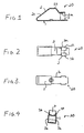
- Figure 1 is a vertical longitudinal cross-sectional view showing one embodiment of a ground terminal according to the device of the present invention.
- Figure 2 is a plan view showing the embodiment of Figure 1.
- Figure 3 is a bottom view showing the embodiment of Figure 1.
- Figure 4 is a side view showing the embodiment of Figure 1.
- Figures 5A and 5B are a cross-sectional view showing the embodiment of Figure 1 under use.
- Figures 6A and 6B are cross-sectional views showing a conventional ground terminal of the prior art.
-
- Hereinafter, the device will be explained based on the embodiments shown in the drawings. Figures 1 through 5 show the preferred embodiments in accordance with the device of the present invention.
- The
ground terminal 20 of the device of the present invention comprises a board portion 1 and aspring contact 2. The board portion 1 may be mounted on a ground pattern (not shown) on a printed circuit board by soldering or other mounting technique. Thespring contact 2 projects integrally from and opposite to the direction of the board portion 1 from one side of the board portion. It is contemplated that the underside of the board portion 1 is preferably plated for improved solderability. - The spring contact comprises an end portion 2a, a first body portion 2b which is configured by being integrally connected to the end portion and extends therefrom such that the first body portion 2b is opposed to the board portion 1, and a
second body portion 2c which couples the first body portion with the board portion. - The
ground terminal 20 is further provided with anengaging wall 3 which stands up integrally from said board portion 1 and engages the end portion 2a of said spring contact. In the embodiment shown in the drawings, theengaging wall 3 specifically operates as a stop wherein the end of theengaging wall 3 holds the end portion 2a of the spring contact. The engaging walls compriseside walls 3a standing up integrally from the opposite sides of said board portion andupper walls 3b extending integrally from the side walls such that the upper walls are opposed to each other, and thus engage the both side of the end portion of the spring contact. - The board portion is soldered to a ground pattern on a printed circuit board. The board portion is provided with through holes 11 such that the soldered joint can be reliable in its strength and in its position accuracy.
- Figures 5A and 5B shows the
ground terminal 20 according to the embodiment of the present invention, which is placed on printedcircuit board 10. In the illustration, the board portion 1 of theground terminal 20 is secured to a ground pattern on a printed circuit board by soldering. More specifically, a plurality of theground terminals 20 are placed on a table. An automatic machine (not shown) absorbs the first body portion of a spring contact by using vacuum and at the same time carries it to a predetermined position in the printed circuit board, and there, by releasing the vacuum absorption, the terminal is placed with the underside thereof down on the circuit board. Then, by passing the circuit board through a soldering bath, the terminal is soldered onto the primed circuit board as well as other circuit elements on the printed circuit board. - After that, the
ground terminal 20 is brought into contact with the shielding panel, chassis, frame or the like in order to ground the ground pattern on the printed circuit board thereto. This work is performed by housing the circuit board via the ground terminal of the device into a casing that is provided, for example, with a shielding panel inside thereof. As the board enters the casing, the spring contact is pressed down toward the side of the board portion (inside), so that the end portion of the spring contact may be separated from the engaging wall. This condition can keep the ground terminal in enough contact with the shielding panel. - Under this condition, the part of the spring contact to contact the shielding panel is required to be, even under contact with the shielding panel, higher than the end of the engaging wall, as well as under non-contact condition. Therefore, there is a permissible range within the movable step (oscillation range ) of the spring contact.
- Although the configuration of the present device has been described above, the following specific advantages can result from the configuration.
- The ground terminal according to the device of the present invention is provided with an engaging wall that stands up integrally from the board portion to engage the end portion of the spring contact. Thus, the engaging wall operates as a stopper against irregular external forces applied when a finger or the like touches the ground terminal, to protect the terminal from deformation. Therefore, the ground terminal according to the present device can eliminate disadvantages such as poor contact made between deformed spring contacts and chassis, and obstacles to housing operations caused by the deformed spring contacts hitched on chassis when boards are housed in chassis.
- Similar to elements for other printed circuits, since the ground terminal of the present. device can be mounted on the circuit board, automatic machines can be used. Accordingly, it is possible to reduce the number of operation processes without any person.
- As described above, the use of the ground terminal of the device provides many advantages and so is useful for taking measures against noise and EMI in various electronics equipment, such as displays using CRT, TFT and STN color liquid crystal.
- Various changes to the foregoing described and shown structures would now be evident to those skilled in the art. Accordingly, the particularly disclosed scope of the invention is set forth in the following claims.
Claims (3)
- A ground terminal comprising:a board to be mounted to a ground pattern on a printed circuit board; anda spring contact projecting integrally and opposite to the direction of said board portion from one side of said board portion,said ground terminal further including an engaging wall which stands up integrally from said portion and engages the end portion of said spring contact.
- The ground terminal according to claim 1 wherein said engaging wall defines a stop wherein the end of said engaging wall holds the end portion of said spring contact.
- The ground terminal according to claim 1 wherein said engaging wall stands up integrally from the opposite sides of said board portion and engages the both sides of the end portion of said spring contact.
Applications Claiming Priority (2)
| Application Number | Priority Date | Filing Date | Title |
|---|---|---|---|
| JP1999004152U JP3064756U (en) | 1999-06-10 | 1999-06-10 | Earth terminal |
| JP41529999 | 1999-06-10 |
Publications (3)
| Publication Number | Publication Date |
|---|---|
| EP1059702A2 true EP1059702A2 (en) | 2000-12-13 |
| EP1059702A3 EP1059702A3 (en) | 2002-07-17 |
| EP1059702B1 EP1059702B1 (en) | 2006-07-26 |
Family
ID=11576798
Family Applications (1)
| Application Number | Title | Priority Date | Filing Date |
|---|---|---|---|
| EP00304317A Expired - Lifetime EP1059702B1 (en) | 1999-06-10 | 2000-05-22 | Ground terminal |
Country Status (4)
| Country | Link |
|---|---|
| US (1) | US20020013096A1 (en) |
| EP (1) | EP1059702B1 (en) |
| JP (1) | JP3064756U (en) |
| KR (1) | KR100662037B1 (en) |
Cited By (4)
| Publication number | Priority date | Publication date | Assignee | Title |
|---|---|---|---|---|
| EP1220364A2 (en) * | 2000-12-28 | 2002-07-03 | J.S.T. Mfg. Co., Ltd. | Connecting terminal and method of mounting the same onto a circuit board |
| FR2930375A1 (en) * | 2008-04-22 | 2009-10-23 | Composants Electr Sa Soc D | DEVICE FOR GROUNDING AND MECHANICAL CONNECTION BETWEEN AN ELECTRONIC CIRCUIT OF AN ADAPTER FOR A VEHICLE ANTENNA AND A SUPPORT HOUSING |
| US8047879B2 (en) | 2009-01-26 | 2011-11-01 | Commscope, Inc. Of North Carolina | Printed wiring boards and communication connectors having series inductor-capacitor crosstalk compensation circuits that share a common inductor |
| CN105048137A (en) * | 2014-04-22 | 2015-11-11 | Smk株式会社 | Terminal for connection of circuit boards |
Families Citing this family (9)
| Publication number | Priority date | Publication date | Assignee | Title |
|---|---|---|---|---|
| US6799177B1 (en) * | 1999-05-05 | 2004-09-28 | Verizon Corporate Services Group Inc. | Systems and methods for securing extranet transactions |
| JP3452546B2 (en) | 2000-12-18 | 2003-09-29 | 北川工業株式会社 | Conductive material |
| US8455994B2 (en) * | 2002-01-31 | 2013-06-04 | Imbera Electronics Oy | Electronic module with feed through conductor between wiring patterns |
| KR101003366B1 (en) * | 2005-11-17 | 2010-12-23 | 주식회사 만도 | Chassis ground open sensing apparatus of automobile |
| JP5555610B2 (en) * | 2010-11-19 | 2014-07-23 | 日本板硝子株式会社 | Terminal, glass plate with terminal and glass plate with terminal for moving body |
| KR101309404B1 (en) * | 2011-11-16 | 2013-09-17 | 황용태 | A connecting apparatus for a terminal |
| JP7076132B2 (en) * | 2018-05-02 | 2022-05-27 | 北川工業株式会社 | contact |
| JP7289497B2 (en) * | 2018-11-15 | 2023-06-12 | 竹内工業株式会社 | surface mount contact |
| KR102484924B1 (en) * | 2021-08-26 | 2023-01-06 | 에코캡 주식회사 | Earth terminal having structure for preventingdeformation of diffusion |
Citations (1)
| Publication number | Priority date | Publication date | Assignee | Title |
|---|---|---|---|---|
| EP0954067A2 (en) * | 1998-04-30 | 1999-11-03 | Kitagawa Industries Co., Ltd. | Grounding terminal and mounting structure of the same on a printed circuit board |
-
1999
- 1999-06-10 JP JP1999004152U patent/JP3064756U/en not_active Expired - Lifetime
- 1999-11-09 US US09/436,855 patent/US20020013096A1/en not_active Abandoned
-
2000
- 2000-05-22 EP EP00304317A patent/EP1059702B1/en not_active Expired - Lifetime
- 2000-05-23 KR KR1020000027770A patent/KR100662037B1/en not_active IP Right Cessation
Patent Citations (1)
| Publication number | Priority date | Publication date | Assignee | Title |
|---|---|---|---|---|
| EP0954067A2 (en) * | 1998-04-30 | 1999-11-03 | Kitagawa Industries Co., Ltd. | Grounding terminal and mounting structure of the same on a printed circuit board |
Cited By (8)
| Publication number | Priority date | Publication date | Assignee | Title |
|---|---|---|---|---|
| EP1220364A2 (en) * | 2000-12-28 | 2002-07-03 | J.S.T. Mfg. Co., Ltd. | Connecting terminal and method of mounting the same onto a circuit board |
| EP1220364A3 (en) * | 2000-12-28 | 2003-09-10 | J.S.T. Mfg. Co., Ltd. | Connecting terminal and method of mounting the same onto a circuit board |
| FR2930375A1 (en) * | 2008-04-22 | 2009-10-23 | Composants Electr Sa Soc D | DEVICE FOR GROUNDING AND MECHANICAL CONNECTION BETWEEN AN ELECTRONIC CIRCUIT OF AN ADAPTER FOR A VEHICLE ANTENNA AND A SUPPORT HOUSING |
| EP2120294A1 (en) * | 2008-04-22 | 2009-11-18 | Societe de Composants Electriques | Device for earth connection and mechanical bonding between an electronic circuit of an adapter for a vehicle antenna and a support box |
| US8047879B2 (en) | 2009-01-26 | 2011-11-01 | Commscope, Inc. Of North Carolina | Printed wiring boards and communication connectors having series inductor-capacitor crosstalk compensation circuits that share a common inductor |
| TWI462502B (en) * | 2009-01-26 | 2014-11-21 | Commscope Inc | Printed wiring boards and communication connectors having series inductor-capacitor crosstalk compensation circuits that share a common inductor |
| CN105048137A (en) * | 2014-04-22 | 2015-11-11 | Smk株式会社 | Terminal for connection of circuit boards |
| CN105048137B (en) * | 2014-04-22 | 2017-11-24 | Smk株式会社 | Circuit substrate terminal for connecting |
Also Published As
| Publication number | Publication date |
|---|---|
| EP1059702B1 (en) | 2006-07-26 |
| KR100662037B1 (en) | 2006-12-28 |
| KR20010007110A (en) | 2001-01-26 |
| JP3064756U (en) | 2000-01-21 |
| EP1059702A3 (en) | 2002-07-17 |
| US20020013096A1 (en) | 2002-01-31 |
Similar Documents
| Publication | Publication Date | Title |
|---|---|---|
| EP1059702B1 (en) | Ground terminal | |
| US11032954B2 (en) | Shield can | |
| US4628412A (en) | Case for shielding electronic devices | |
| US6670559B2 (en) | Electromagnetic shield for printed circuit boards | |
| KR100489860B1 (en) | A method and a device for shielding of electronic components on a circuit board | |
| KR101390191B1 (en) | Electronic device with capacity of electrostatic discharge | |
| US8520405B2 (en) | Shield case and image display device | |
| US6504727B1 (en) | Earphone jack holding device | |
| JP3851526B2 (en) | Earth terminal | |
| JP3192570B2 (en) | Ground terminal | |
| KR200456269Y1 (en) | Clip type terminal | |
| KR101397284B1 (en) | Contactor inserted into printed circuit board and connection structure thereof | |
| EP1014774B1 (en) | Earthing contact | |
| EP0957665B1 (en) | Electronic device | |
| KR100649491B1 (en) | An apparatus for fixing a shield case to a circuit board | |
| JP3752382B2 (en) | Electronics | |
| KR100272805B1 (en) | An electronic device | |
| JPH0716116B2 (en) | Electronic device | |
| US20210296805A1 (en) | Card Connector Assemblies with Integrated Component Shielding | |
| KR100633087B1 (en) | Eletric and electronic device | |
| EP2473012A1 (en) | Combining printed circuit boards | |
| KR100633088B1 (en) | Eletric and electronic device | |
| HAUTER | Surface mounted device influence on equipment reliability | |
| JPH062301Y2 (en) | Parts mounting device | |
| JPH0310630Y2 (en) |
Legal Events
| Date | Code | Title | Description |
|---|---|---|---|
| PUAI | Public reference made under article 153(3) epc to a published international application that has entered the european phase |
Free format text: ORIGINAL CODE: 0009012 |
|
| AK | Designated contracting states |
Kind code of ref document: A2 Designated state(s): AT BE CH CY DE DK ES FI FR GB GR IE IT LI LU MC NL PT SE |
|
| AX | Request for extension of the european patent |
Free format text: AL;LT;LV;MK;RO;SI |
|
| RAP1 | Party data changed (applicant data changed or rights of an application transferred) |
Owner name: THOMAS & BETTS INTERNATIONAL, INC. |
|
| PUAL | Search report despatched |
Free format text: ORIGINAL CODE: 0009013 |
|
| AK | Designated contracting states |
Kind code of ref document: A3 Designated state(s): AT BE CH CY DE DK ES FI FR GB GR IE IT LI LU MC NL PT SE |
|
| AX | Request for extension of the european patent |
Free format text: AL;LT;LV;MK;RO;SI |
|
| RIC1 | Information provided on ipc code assigned before grant |
Free format text: 7H 01R 13/658 A, 7H 01R 12/16 B, 7H 05K 9/00 B, 7H 01R 4/64 B |
|
| 17P | Request for examination filed |
Effective date: 20030107 |
|
| AKX | Designation fees paid |
Designated state(s): DE FR GB IT |
|
| 17Q | First examination report despatched |
Effective date: 20050422 |
|
| GRAP | Despatch of communication of intention to grant a patent |
Free format text: ORIGINAL CODE: EPIDOSNIGR1 |
|
| GRAS | Grant fee paid |
Free format text: ORIGINAL CODE: EPIDOSNIGR3 |
|
| GRAA | (expected) grant |
Free format text: ORIGINAL CODE: 0009210 |
|
| AK | Designated contracting states |
Kind code of ref document: B1 Designated state(s): DE FR GB IT |
|
| PG25 | Lapsed in a contracting state [announced via postgrant information from national office to epo] |
Ref country code: IT Free format text: LAPSE BECAUSE OF FAILURE TO SUBMIT A TRANSLATION OF THE DESCRIPTION OR TO PAY THE FEE WITHIN THE PRESCRIBED TIME-LIMIT;WARNING: LAPSES OF ITALIAN PATENTS WITH EFFECTIVE DATE BEFORE 2007 MAY HAVE OCCURRED AT ANY TIME BEFORE 2007. THE CORRECT EFFECTIVE DATE MAY BE DIFFERENT FROM THE ONE RECORDED. Effective date: 20060726 |
|
| REG | Reference to a national code |
Ref country code: GB Ref legal event code: FG4D |
|
| REF | Corresponds to: |
Ref document number: 60029514 Country of ref document: DE Date of ref document: 20060907 Kind code of ref document: P |
|
| ET | Fr: translation filed | ||
| PLBE | No opposition filed within time limit |
Free format text: ORIGINAL CODE: 0009261 |
|
| STAA | Information on the status of an ep patent application or granted ep patent |
Free format text: STATUS: NO OPPOSITION FILED WITHIN TIME LIMIT |
|
| 26N | No opposition filed |
Effective date: 20070427 |
|
| PGFP | Annual fee paid to national office [announced via postgrant information from national office to epo] |
Ref country code: DE Payment date: 20090528 Year of fee payment: 10 Ref country code: FR Payment date: 20090518 Year of fee payment: 10 |
|
| PGFP | Annual fee paid to national office [announced via postgrant information from national office to epo] |
Ref country code: GB Payment date: 20090528 Year of fee payment: 10 |
|
| GBPC | Gb: european patent ceased through non-payment of renewal fee |
Effective date: 20100522 |
|
| REG | Reference to a national code |
Ref country code: FR Ref legal event code: ST Effective date: 20110131 |
|
| PG25 | Lapsed in a contracting state [announced via postgrant information from national office to epo] |
Ref country code: DE Free format text: LAPSE BECAUSE OF NON-PAYMENT OF DUE FEES Effective date: 20101201 |
|
| PG25 | Lapsed in a contracting state [announced via postgrant information from national office to epo] |
Ref country code: FR Free format text: LAPSE BECAUSE OF NON-PAYMENT OF DUE FEES Effective date: 20100531 |
|
| PG25 | Lapsed in a contracting state [announced via postgrant information from national office to epo] |
Ref country code: GB Free format text: LAPSE BECAUSE OF NON-PAYMENT OF DUE FEES Effective date: 20100522 |