EP1058493A2 - Socket for electrical parts - Google Patents
Socket for electrical parts Download PDFInfo
- Publication number
- EP1058493A2 EP1058493A2 EP00111583A EP00111583A EP1058493A2 EP 1058493 A2 EP1058493 A2 EP 1058493A2 EP 00111583 A EP00111583 A EP 00111583A EP 00111583 A EP00111583 A EP 00111583A EP 1058493 A2 EP1058493 A2 EP 1058493A2
- Authority
- EP
- European Patent Office
- Prior art keywords
- electrical part
- contact
- solder ball
- contact portion
- socket
- Prior art date
- Legal status (The legal status is an assumption and is not a legal conclusion. Google has not performed a legal analysis and makes no representation as to the accuracy of the status listed.)
- Granted
Links
- 229910000679 solder Inorganic materials 0.000 claims abstract description 109
- 238000006073 displacement reaction Methods 0.000 claims abstract description 34
- 230000036316 preload Effects 0.000 description 12
- 238000012986 modification Methods 0.000 description 5
- 230000004048 modification Effects 0.000 description 5
- 230000000694 effects Effects 0.000 description 2
- 230000002093 peripheral effect Effects 0.000 description 2
- 230000005489 elastic deformation Effects 0.000 description 1
- 238000003780 insertion Methods 0.000 description 1
- 230000037431 insertion Effects 0.000 description 1
- 238000011056 performance test Methods 0.000 description 1
- 239000004065 semiconductor Substances 0.000 description 1
Images






Classifications
-
- H—ELECTRICITY
- H01—ELECTRIC ELEMENTS
- H01R—ELECTRICALLY-CONDUCTIVE CONNECTIONS; STRUCTURAL ASSOCIATIONS OF A PLURALITY OF MUTUALLY-INSULATED ELECTRICAL CONNECTING ELEMENTS; COUPLING DEVICES; CURRENT COLLECTORS
- H01R13/00—Details of coupling devices of the kinds covered by groups H01R12/70 or H01R24/00 - H01R33/00
- H01R13/62—Means for facilitating engagement or disengagement of coupling parts or for holding them in engagement
- H01R13/629—Additional means for facilitating engagement or disengagement of coupling parts, e.g. aligning or guiding means, levers, gas pressure electrical locking indicators, manufacturing tolerances
- H01R13/62983—Linear camming means or pivoting lever for connectors for flexible or rigid printed circuit boards, flat or ribbon cables
- H01R13/62994—Lever acting on a connector mounted onto the flexible or rigid printed circuit boards, flat or ribbon cables
-
- H—ELECTRICITY
- H05—ELECTRIC TECHNIQUES NOT OTHERWISE PROVIDED FOR
- H05K—PRINTED CIRCUITS; CASINGS OR CONSTRUCTIONAL DETAILS OF ELECTRIC APPARATUS; MANUFACTURE OF ASSEMBLAGES OF ELECTRICAL COMPONENTS
- H05K7/00—Constructional details common to different types of electric apparatus
- H05K7/02—Arrangements of circuit components or wiring on supporting structure
- H05K7/10—Plug-in assemblages of components, e.g. IC sockets
- H05K7/1053—Plug-in assemblages of components, e.g. IC sockets having interior leads
- H05K7/1076—Plug-in assemblages of components, e.g. IC sockets having interior leads co-operating by sliding
- H05K7/1084—Plug-in assemblages of components, e.g. IC sockets having interior leads co-operating by sliding pin grid array package carriers
-
- H—ELECTRICITY
- H05—ELECTRIC TECHNIQUES NOT OTHERWISE PROVIDED FOR
- H05K—PRINTED CIRCUITS; CASINGS OR CONSTRUCTIONAL DETAILS OF ELECTRIC APPARATUS; MANUFACTURE OF ASSEMBLAGES OF ELECTRICAL COMPONENTS
- H05K7/00—Constructional details common to different types of electric apparatus
- H05K7/02—Arrangements of circuit components or wiring on supporting structure
- H05K7/10—Plug-in assemblages of components, e.g. IC sockets
- H05K7/1007—Plug-in assemblages of components, e.g. IC sockets with means for increasing contact pressure at the end of engagement of coupling parts
Definitions
- the present invention relates to a socket for an electrical part for detachably holding an electrical part such as a semiconductor device (called as "IC package” hereinafter).
- the present invention relates to a socket for an electrical part, which is adapted to prevent a contact portion of a contact pin from being stuck to a solder ball that is a terminal of the electrical part.
- an IC socket for detachably holding an IC package as "electrical part".
- the IC package includes a BGA (Ball Grid Array) type of IC package which has a rectangular-shaped package body and a large number of solder balls mounted on a bottom surface of the package body.
- BGA All Grid Array
- a contact pin is disposed to the IC socket and, to the contact pin, a pair of elastic pieces is formed.
- a contact portion is formed to one end portion of each of the elastic pieces so as to be contacted to a side portion of the solder ball and separated therefrom.
- One of the paired elastic pieces is pressed by a movable plate sliding in a horizontal direction to be elastically deformed thereby.
- the movable plate After the inserting work, the movable plate is returned to the original position so that the contact portion of one of the paired elastic pieces is returned to an original position at which no pressing force by the movable plate is applied, whereby the solder ball is clamped by both of the contact portions to electrically connected thereto.
- both of the contact portions thereof are separated from the solder ball and, thereafter, the IC package is removed from the IC socket with an automatic machine.
- the IC package is heated at approximately 125° C so that the solder ball gets to be softened to frequently be stuck to at least one of the contact portions.
- the solder ball In a state that the solder ball is stuck to at least one of the contact portions, when deforming one of the paired elastic pieces to widen the interval between both of the contact portions, in some cases, the solder ball is not separated from at least one of the contact portions with being stuck thereto.
- a socket for an electrical part comprising:
- the stopper means is contacted to the moving electrical part to stop the electrical part, and the displacement length of the contact pin is longer than the length of movement of the electrical part to the stopper means, it is possible to surely remove the contact portion from the solder ball. Therefore, it is permitted to prevent the contact portion from being stuck to the solder ball, making it possible to remove the electrical part from the socket therefor without using extracting force.
- the contact pin has a pair of elastic pieces formed at front end portions thereof with a pair of contact portions, one of the contact portions of one of the elastic pieces being formed so that it is easy for the solder ball to be stuck to one of the contact portions, as compared with another one of the contact portions of another one of the elastic pieces, and the stopper means is formed on one side portion of the socket body, so that when the solder ball of the electrical part is stuck to one of the contact portions of one of the elastic pieces, the electrical part moving in accordance with the displacement of one of the contact portions is contacted to the stopper means.
- the solder ball it is easy for the solder ball to be stuck to one of the contact portions, as compared with another one of the contact portions of another one of the elastic pieces.
- the stopper means is formed on the one side portion of the socket body, so that, when the solder ball of the electrical part is stuck to one of the contact portions of one of the elastic pieces, the electrical part moving in accordance with the displacement of one of the contact portions is contacted to the stopper means.
- the movable plate is adapted to be movable in a direction substantially parallel to the mount surface
- one of the elastic pieces is a movable side elastic piece elastically movable by the movable plate
- another one of the elastic pieces is a stationary side elastic piece
- the stopper means is formed on the one side portion of the socket body so that, when the solder ball of the electrical part is stuck to the contact portion of the movable side elastic piece, the electrical part moving in accordance with the displacement of the contact portion of the movable side elastic piece is contacted to the stopper means.
- the socket having the structure in that the movable plate is moved in parallel to the mount surface.
- the contact portion of the elastic piece of the contact pin is formed with a projection portion adapted to bite into a side surface of the solder ball so that it is easy for the solder ball to be stuck to the contact portion.
- the contact portion by forming on the contact portion only the projection portion adapted to bite into the side surface of the solder ball, it is easy to stick the solder ball of the electrical part to the contact portion, making it possible to improve the reliability of removing the contact portion from the solder ball.
- the contact portion has a substantially rod shape and adapted to bite into a side surface of the solder ball so that it is easy for the solder ball to be stuck to the contact portion.
- the contact portion has a substantially rod shape, it is possible to render the contact portion bite into the side surface of the solder ball.
- a socket for an electrical part comprising:
- the contact pin has a pair of elastic pieces formed at front end portions thereof with a pair of contact portions, one of the contact portions of one of the elastic pieces being provided with a press portion for pressing the solder ball, and the stopper means is formed on one side portion of the socket body so that, when the electrical part moves in accordance with the displacement of one of the contact portions, while the solder ball is pressed to be fit to the press portion of one of the contact portions, the electrical part moving in accordance with the displacement of one of the contact portions is contacted to the stopper means.
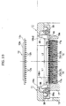
- Fig. 1 to Fig. 14B represent the first embodiment of the present invention, in which reference numeral 11 denotes an IC socket as "socket for electrical parts".
- the IC socket 11 electrically connects solder balls 12b as "terminals" of the IC package 12 to a printed circuit board (not shown) of a measuring device such as tester.
- This IC package 12 is called as Ball Grid Array (BGA) type.
- the BGA type of IC package 12 is provided with a package body 12a having, for example, a substantially square shape.
- the IC package 12 is also provided with a plurality of solder balls 12b each having a substantially spherical shape and mounted on a bottom (lower) surface of the package body 12a so as to project downward therefrom.
- the solder balls 12b are arranged to provide a matrix-shape (grid array).
- the IC socket 11 is provided with a socket body 13 mounted on the printed circuit board and a plurality of contact pins 15.
- the contact pins 15 are arranged in a matrix-shape (grid array) similar to the solder balls and permitted to be contacted to or separated from the solder balls 12b, respectively.
- the IC socket 11 is also provided with a preload plate 16 through which the contact pins 15 are inserted, a slide plate 17 as "movable plate” and a top plate 18.
- the preload plate 16, the slide plate 17 and the top plate 18 are mounted on an upper side of the socket body 13 so as to be successively laminated in an upward direction of the socket body 13.
- an operation member 19 is arranged for making the slide plate 17 slide in a horizontal direction.
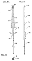
- the contact pin 15 has an elasticity or springy property and is formed in such a manner that a plate member having a superior conductivity is pressed through a press working so as to provide a shape as shown in Figs. 5A-5C, Fig. 6 and Figs. 7A-7C.
- the contact pin 15 is formed, at its upper end side, with a stationary side elastic piece 15h and a movable side elastic piece 15i (a pair of elastic pieces) and, at its lower end side, with one integrated solder tail portion 15b.
- a stationary side elastic piece 15h and a movable side elastic piece 15i (a pair of elastic pieces) and, at its lower end side, with one integrated solder tail portion 15b.
- the stationary side elastic piece will be referred simply to the stationary elastic piece and the movable side elastic piece will be also referred simply to the movable elastic piece.
- the contact pin 15 is also provided, at its lower side of the elastic pieces 15h and 15i, with a base portion 15c so that the elastic pieces 15h and 15i are integrated thereby.
- the elastic pieces 15h and 15i extend upward from the base portion 15c and the solder tail portion 15b extends downward therefrom.
- the base portion 15c is bent so as to have a substantially U-shape in its lateral cross section so that the elastic pieces 15h and 15i branch from the base portion 15c and that the elastic pieces 15h and 15i are opposite to each other.
- Each of the elastic pieces 15h and 15i is formed at its uppermost end (front end) with a contact portion 15d so that each contact portion 15d is contacted to a side surface portion of the solder ball 12b or separated therefrom, whereby the solder ball 12b is adapted to be clamped in the contact portions 15d of the elastic pieces 15h and 15i.
- the contact portion 15d of the movable elastic piece 15i as "one of elastic pieces” is formed with a pair of inclined surfaces 15m and a projection portion 15n.
- the paired inclined surfaces 15m are arranged in substantially tangential directions at contact positions of the solder ball 12b to the contact portion 15d.
- the projection portion 15n has a substantially triangular shape and is formed between the paired inclined surfaces 15m.
- the contact portion 15d of the stationary elastic piece 15h as "another one of elastic piece” is formed with an inclined surface 15j and an orthogonal surface 15k.
- the inclined surface 15j is arranged to be inclined at a predetermined angle with respect to a direction Q orthogonal to a displacement direction P of the movable elastic piece 15i, and the orthogonal surface 15k is arranged to extend to the inclined surface 15j and to be orthogonal to the displacement direction P.
- the projection portion 15n of the contact portion 15d of the movable elastic piece 15i is adapted to press the solder ball 12b so that the solder ball 12b is fit to the projection portion 15n, the solder ball 12b bites into the projection portion 15n of the movable elastic piece 15i. Therefore, the contact portion 15d of the movable elastic piece 15i is formed so that it is easy for the solder ball 12b to be stuck to the contact portion 15d of the movable elastic piece 15i, as compared with the contact portion 15d of the stationary elastic piece 15h.
- the elastic pieces 15h and 15i of the contact pin 15 are provided with bent portions 15e, respectively.
- the bent portions 15e of the respective elastic pieces 15h and 15i are formed at respective middle portions thereof so that the respective middle portions of the elastic pieces 15h and 15i are bent far from each other. Vertex portions of the respective bent portions 15e are pressed by the preload plate 16. While the bent portions 15e are not subjected to any external force, as shown in Fig. 5A, a width (interval) H1 formed between the respective vertex portions of the bent portions 15e of the paired elastic pieces 15h and 15i is made wider than a width (interval) H2 formed between respective top ends of the paired contact portions 15d thereof.
- press-fit holes 13a are formed through the socket body 13a and through holes are formed through the printed circuit board (not shown).
- solder tail portion 15b and the base portion 15c of the contact pin 15 are integrally pressed to fit in the press-fit hole 13a so that the solder tail portion 15b projects downward therefrom.
- the projecting solder tail portion 15b further projects downward through a locate board 21 so as to be inserted into the through hole.
- Each of the solder tail portions 15b of each of the contact pins 15 is inserted in each of the through holes of the printed circuit board, so that each of the solder tail portions 15b is soldered to be electrically connected to the printed circuit board.
- the preload plate 16 is detachably mounted on the socket body 13 and, through the preload plate 16, preload holes 16a are formed so that each of the paired elastic pieces 15h and 15i is inserted in each of the preload holes 16a.
- a diameter of the preload hole 16a is set so that, in a state that each of the paired elastic pieces 15h and 15i is inserted in each of the preload holes 16a, the preload hole 16a is adapted to previously press the paired elastic pieces 15h and 15i in a direction as the contact portions 15d of the elastic pieces 15h and 15i are close to each other.
- bent portion 15e is formed on each of the paired elastic pieces 15h and 15i, while each of the paired elastic pieces 15h and 15i is inserted in each of the preload holes 16a, the vertex portions of the bent portions 15e are pressed by an inner wall of the preload hole 16a.
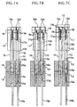
- the slide plate 17 is arranged to be slidable in a right and left direction (a slide direction in substantially parallel to a mount surface portion 18a of the top plate 18) in Fig. 2, Figs. 7A-7C.
- the movable elastic piece 15i of the contact pin 15 is elastically deformed so as to displace the contact portion 15d in a predetermined length.
- the predetermined length of the displacement of the contact portion 15d of the movable elastic piece 15i is described hereinafter.
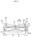
- the operation member 19 and the slide plate 17 are mechanically connected through X-shaped links 22 shown in Figs. 2 and 9 so that, when the operation member 19 is moved vertically, the slide plate 17 is slid in the right and left direction by operations of the X-shaped links 22.
- the slide plate 17 is provided with a press portion 17a adapted to press the movable elastic piece 15i so as to elastically deform the movable elastic piece 15i.
- the X-shaped links 22 are disposed correspondingly to both side surface portions of the square shaped slide plate 17.
- the X-shaped link 22, as shown in Figs. 2 and 9, is provided with a first link member 23 and a second link member 25 each having a same length.
- the first link member 23 and the second link member 25 are rotatably joined by a central joint pin 27.
- the first link member 23 has a lower end portion 23a in Fig. 9, that is, one end portion 23a of the socket body side, and the lower end portion 23a is pivotally joined to the socket body 13 by a lower end joint pin 29.
- the second link member 25 has a lower end portion 25a of the socket body side, and the slide plate 17 has one end portion in the slide direction thereof.
- the lower end portion 25a of the second link member 25 is rotatably joined to the one end portion of the slide plate 17 by a lower end joint pin 30.
- Upper end portions 23b and 25b, that is, other end portions opposite to the one end portions 23a and 25a of the first and second link members 23 and 25 are joined to the operation member 19 by upper joint pins 33 and 34, respectively.
- the first link member 23 is formed at its upper end portion 23b with a slot 23c so that the first link member 23 is joined through the slot 23c to the operation member 17 by the upper joint pin 33.
- the top plate 18 is provided with a mount surface portion 18a on which the IC package 12 is mounted.
- the top plate 18 is also provided with guide portions 18b1 and 18b2 for arranging the IC package 12 to a predetermined position on the mount surface portion 18a.
- one pair of guide portions 18b1 are mounted on the mount surface portion 18a in correspondence with one pair of corner portions of the IC package 12
- other pair of guide portions 18b2 are mounted on the mount surface 18a in correspondence with other pair of corner portions of the IC package 12.
- the one pair of guide portions 18b1 is opposite to the other pair of guide portions 18b2 in the right and left direction (displacement direction of the contact portion 15d).
- the one pair of guide portions 18b1 is arranged on one side (left side) of the mount surface portion 18a with respect to a center thereof, and the other pair of guide portions 18b2 is arranged on other side (right side) of the mount surface portion 18a with respect to the center thereof.
- the one pair of guide portions 18b1 and the other pair of guide portions 18b2 are arranged so that a distance L1 between a middle point of the guide portions 18b1 and the center of the mount surface portion 18a is different from a distance L2 between a middle point of the guide portions 18b2 and the center thereof. Then, in this embodiment, the distance L2 is slightly shorter than the distance L1.
- Each of the guide portions 18b2 is provided with an inner wall surface on which a stopper portion 18e is formed.
- the contact portion 15d of the movable elastic piece 15i When the contact portion 15d of the movable elastic piece 15i is displaced by the slide of the slide plate 17, the contact portion 15d is stuck to the solder ball 12b so that, when the package body 12a is moved according to the displacement of the contact portion 15d of the movable elastic piece 15i, the package body 12a is contacted to the stopper portions 18e of the guide portions 18b2 so as to be stopped.
- a displacement length of the contact portion 15d of the movable elastic piece 15i by the slide plate 17 is set to be longer than that of the package body 12a which is displaced to be contacted up to the stopper portions 18e.
- the top plate 18 is formed with positioning portions 18c.
- Each of the positioning portions 18c is arranged to be inserted between each of the paired contact portions 15d of each of the contact pins 15.
- the positioning portion 18c has a function for positioning the paired contact portions 15d of each of the contact pins 15.
- the positioning portion 18c is clamped with the elastic pieces 15h and 15i so as to be held thereby.
- the operation member 19, as shown in Figs. 1, 2 and so on, is provided with an opening 19a having a predetermined area which allows the IC package 12 to be inserted therein.
- the IC package 12 is inserted through the opening 19a so as to be mounted on the mount surface 18a, so that the IC package 12 is located at the predetermined position defined by the guide portions 18b1 and 18b2.
- the operation member 19, as shown in Fig. 3, is arranged to be movable vertically with respect to the socket body 13 and is urged upward by springs 36.
- the operation member 19 is also formed with a pair of operative convex portions 19b for rotating a pair of latch members 38.
- each of the latch members 38 is disposed through a shaft 38a to the socket body 13 so as to be rotatable about the shaft 38a.
- the latch members 38 are urged by springs 39 toward the center of the socket body 13, respectively.
- Each of the latch members 38 is provided with a holding portion 38b for holding a peripheral portion 12c of the IC package 12 mounted at the predetermined position on the mount surface 18a.
- Each of the latch members 38 is also formed with a press portion 38c permitted to be pressed by the convex portion 19b of the operation member 19.
- Each of the contact pins 15 carries out substantially the same movement, and accordingly, only the movement of only one of the contact pins 15 will be explained.
- the deformation of the movable elastic piece 15i due to the elastic deformation makes open the paired contact portions 15d of the elastic pieces 15h and 15i as shown in Fig. 7B.
- each of the latch members 38 is pressed by the convex portion 19b of the operation member 19 so that each of the latch members 38 rotates outward from the socket body 13 towards the withdrawal position against the urging force of the spring 39, thereby displacing the holding portion 38b of each of the latch members 38 to the withdrawal position, as shown in Fig. 10.
- the IC package 12 is mounted on the mount surface 18a of the top plate 18 so as to be guided by the guide portions 18b1 and 18b2, thereby being set to the predetermined position on the mount surface portion 18a.
- Each of the solder balls 12b is inserted in each of the paired and opened contact portions 15d of each of the contact pins 15 while each of the solder balls 12b is in a non-contact state with each of the paired contact portions 15d.
- each solder ball 12b in each paired contact portion 15d After the insertion of each solder ball 12b in each paired contact portion 15d, when the downward press force applied to the operation member 19 is released, the operation member 19 is moved upward by the urging force of the springs 36, so that the slide plate 17 is slid towards the left direction in Fig. 7A to Fig. 7C by the X-shaped operation link 22, and that each of the latch members 38 is rotated towards the mounted IC package 12 by the urging force of the spring 39.
- the stationary elastic piece 15h is slightly elastically deformed so that the contact portion 15d of the stationary elastic piece 15h is slightly displaced so as to widen the interval between the contact portions 15d of the movable elastic piece 15i and the stationary elastic piece 15h.
- each of the solder balls 12b of the IC package 12 and the printed circuit board on which the IC socket 11 is mounted are electrically connected through each of the contact pins 15 of the IC socket 11.
- the inclined surface 15j of the stationary elastic piece 15h is slid on the solder ball 12b to obtain a wiping effect.
- the printed circuit board on which the IC socket 11 is mounted is set in a burn-in tank.
- the burn-in test of the IC package 12 is carried out.
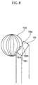
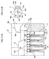
- the temperature in the burn-in tank is increased, the solder ball 12 is softened so that the projection portion 15n of the contact portion 15d of the movable elastic piece 15i bites into the side surface portion of the solder ball 12b, as shown in Figs. 11A and 11B.
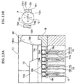
- the displacement length of the contact portion 15d of the movable elastic piece 15i is set so that the contact portion 15d of the movable elastic piece 15i is further displaced from the state that the package body 12a is contacted to the stopper portions 18e, when the movable elastic piece 15i is further elastically deformed from the contacting state thereof to the stopper portions 18e so as to make displace the contact portion 15d of the movable elastic piece 15i in the right direction in Figs. 14A and 14B, the projection portion 15n of the contact portion 15d is separated from the solder ball 12b, making it possible to surely prevent the solder ball 12b from being stuck to the contact portion 15d. As a result, the paired contact portions 15d of the contact pin 15 are separated from the solder ball 12 to make it possible to remove the IC package 12 from the IC socket 11 by the automatic machine without using extracting force.
- Figs. 15A and 15B represent the second embodiment of the present invention.
- the contact portion 15d of the movable elastic piece 15i has a slender rod-shape and a rectangular shape in its lateral cross section so that the contact portion 15d is adapted to bite into the softened solder ball 12b.
- the stationary elastic piece 15i is omitted from Figs. 15A and 15B.
- the present invention is applied to the IC socket as "socket for electrical parts", but the present invention is not limited to this application, and the present invention may be applied to a socket for an electrical part except for the IC package.
- the movable plate is adapted to move in a horizontal direction (in substantially parallel to the mount surface portion), but the present invention is not limited to this structure, and in one modification, the movable plate may be adapted to move in a vertical direction so as to make both of the paired contact portions displace (open and close).
- each pair of the guide portions arranged in the slide direction is provided with the stopper portion 18e.
- Respective displacement lengths of the contact portions of the movable elastic piece and the stationary elastic piece by the slide plate are set to be longer than the displacement length of the package body which is displaced to the stopper portions.
- the stationary elastic piece and the movable elastic piece are formed on the contact pin, but the present invention is applicable to the structure in which the movable elastic piece is formed only on the contact pin.
- the stopper portion is formed to the guide portion of the socket body, but the present invention is not limited to this structure, and the stopper portion may be provided to other portion of the socket body to which the IC package is permitted to be contacted.
Landscapes
- Engineering & Computer Science (AREA)
- Microelectronics & Electronic Packaging (AREA)
- Testing Of Individual Semiconductor Devices (AREA)
- Connecting Device With Holders (AREA)
- Measuring Leads Or Probes (AREA)
Abstract
Description
Claims (7)
- A socket for an electrical part comprising:a socket body having a mount portion on which an electrical part is mounted, said electrical part having a solder ball;a contact pin arranged to the socket body and adapted to be contacted to or separated from the solder ball of the electrical part;a movable plate disposed to the socket body to be movable with respect to the socket body; andstopper means provided for the socket body and adapted to be contacted to the moving electrical part to stop the electrical part at a time when the solder ball of the electrical part is stuck to the contact portion so that the electrical part moves in accordance with the displacement of the contact portion,said contact pin having an elastic piece formed at a front end portion thereof with a contact portion, said contact portion being elastically deformed in accordance with the movement of the movable plate so as to displace the contact portion by a displacement length to separate the contact portion from a side surface of the solder ball, andsaid displacement length of the contact pin being longer than a length of movement of the electrical part to the stopper means.
- A socket for an electrical part according to claim 1, wherein said contact pin has a pair of elastic pieces formed at front end portions thereof with a pair of contact portions, one of said contact portions of one of the elastic pieces being formed so that it is easy for the solder ball to be stuck to one of the contact portions, as compared with another one of the contact portions of another one of the elastic pieces, and wherein said stopper means is formed on one side portion of the socket body so that, when the solder ball of the electrical part is stuck to one of the contact portions of one of the elastic pieces, the electrical part moving in accordance with the displacement of one of the contact portions is contacted to the stopper means.
- A socket for an electrical part according to claim 2, wherein said movable plate is adapted to be movable in a direction substantially parallel to the mount surface, one of said elastic pieces is a movable side elastic piece elastically deformed by the movable plate, another one of said elastic pieces is a stationary side elastic piece, and wherein said stopper means is formed on the one side portion of the socket body so that, when the solder ball of the electrical part is stuck to the contact portion of the movable side elastic piece, the electrical part moving in accordance with the displacement of the contact portion of the movable side elastic piece is contacted to the stopper means.
- A socket for an electrical part according to claim 1, wherein said contact portion of the elastic piece of the contact pin is formed with a projection portion adapted to bite into a side surface of the solder ball so that it is easy for the solder ball to be stuck to the contact portion.
- A socket for an electrical part according to claim 1, wherein said contact portion has a substantially rod shape and is adapted to bite into a side surface of the solder ball so that it is easy for the solder ball to be stuck to the contact portion.
- A socket for an electrical part comprising:a socket body having a mount portion on which an electrical part is mounted, said electrical part having a solder ball;a contact pin arranged to the socket body and adapted to be contacted to or separated from the solder ball of the electrical part;a movable plate disposed to the socket body to be movable with respect to the socket body; andstopper means provided for the socket body and adapted to be contacted to the moving electrical part to stop the electrical part at a time when the electrical part moves in accordance with the displacement of the contact portion while the solder ball is contacted to the contact portion,said contact pin having an elastic piece formed at a front end portion thereof with a contact portion, said contact portion being elastically deformed in accordance with the movement of the movable plate so as to displace the contact portion by a displacement length to separate the contact portion from a side surface of he solder ball.
- A socket for an electrical part according to claim 6, wherein said contact pin has a pair of elastic pieces formed at front end portions thereof with a pair of contact portions, one of said contact portions of one of the elastic pieces being provided with a press portion for pressing the solder ball, and wherein said stopper means is formed on one side portion of the socket body so that, when the electrical part moves in accordance with the displacement of one of the contact portions, while the solder ball is pressed to be fit to the press portion of one of the contact portions, the electrical part moving in accordance with the displacement of one of the contact portions is contacted to the stopper means.
Applications Claiming Priority (2)
| Application Number | Priority Date | Filing Date | Title |
|---|---|---|---|
| JP15183999A JP4087012B2 (en) | 1999-05-31 | 1999-05-31 | Socket for electrical parts |
| JP15183999 | 1999-05-31 |
Publications (3)
| Publication Number | Publication Date |
|---|---|
| EP1058493A2 true EP1058493A2 (en) | 2000-12-06 |
| EP1058493A3 EP1058493A3 (en) | 2002-02-13 |
| EP1058493B1 EP1058493B1 (en) | 2006-06-28 |
Family
ID=15527432
Family Applications (1)
| Application Number | Title | Priority Date | Filing Date |
|---|---|---|---|
| EP00111583A Expired - Lifetime EP1058493B1 (en) | 1999-05-31 | 2000-05-30 | Socket for electrical parts |
Country Status (5)
| Country | Link |
|---|---|
| US (1) | US6261114B1 (en) |
| EP (1) | EP1058493B1 (en) |
| JP (1) | JP4087012B2 (en) |
| KR (1) | KR100365485B1 (en) |
| DE (1) | DE60029052T2 (en) |
Cited By (2)
| Publication number | Priority date | Publication date | Assignee | Title |
|---|---|---|---|---|
| CN107919294A (en) * | 2016-10-07 | 2018-04-17 | 瑞萨电子株式会社 | Method, semi-conductor device manufacturing method and semiconductor devices |
| CN113631931A (en) * | 2019-04-04 | 2021-11-09 | 黄东源 | Coverless BGA socket assembly for semiconductor device testing |
Families Citing this family (27)
| Publication number | Priority date | Publication date | Assignee | Title |
|---|---|---|---|---|
| JP3619413B2 (en) * | 2000-01-18 | 2005-02-09 | 株式会社エンプラス | Socket for electrical parts |
| JP3703741B2 (en) * | 2001-07-04 | 2005-10-05 | 山一電機株式会社 | IC socket |
| JP3822074B2 (en) * | 2001-08-01 | 2006-09-13 | 株式会社エンプラス | Socket for electrical parts |
| JP3678182B2 (en) * | 2001-08-10 | 2005-08-03 | 山一電機株式会社 | Socket for semiconductor device |
| JP2003100408A (en) * | 2001-09-20 | 2003-04-04 | Yamaichi Electronics Co Ltd | IC socket |
| JP3745667B2 (en) * | 2001-10-09 | 2006-02-15 | 山一電機株式会社 | IC socket |
| JP4098231B2 (en) * | 2003-12-19 | 2008-06-11 | 山一電機株式会社 | Socket for semiconductor device |
| US7042239B1 (en) * | 2004-06-25 | 2006-05-09 | Credence Systems Corporation | Arrangement for manual disengagement of a device interface board from a personal tester |
| US7090522B2 (en) * | 2004-08-27 | 2006-08-15 | Aries Electronics, Inc. | Top loaded burn-in socket |
| JP4312685B2 (en) * | 2004-08-31 | 2009-08-12 | 山一電機株式会社 | Semiconductor device attaching / detaching method, semiconductor device attaching / detaching device using the same, and semiconductor device socket |
| US7121860B2 (en) * | 2004-09-02 | 2006-10-17 | Micron Technology, Inc. | Pinch-style support contact, method of enabling electrical communication with and supporting an IC package, and socket including same |
| TWI280693B (en) * | 2004-09-10 | 2007-05-01 | Hon Hai Prec Ind Co Ltd | Electrical connector |
| US20070224867A1 (en) * | 2004-11-08 | 2007-09-27 | Allsup Thomas A | Latching dual contact socketfor testing ball grid array devices |
| JP4471941B2 (en) * | 2005-03-10 | 2010-06-02 | 山一電機株式会社 | Socket for semiconductor device |
| JP4767741B2 (en) * | 2006-04-13 | 2011-09-07 | 株式会社エンプラス | Socket for electrical parts |
| JP2009036679A (en) * | 2007-08-02 | 2009-02-19 | Yamaichi Electronics Co Ltd | Socket for semiconductor device |
| JP4495200B2 (en) * | 2007-09-28 | 2010-06-30 | 山一電機株式会社 | Socket for semiconductor device |
| WO2009084085A1 (en) * | 2007-12-27 | 2009-07-09 | Yamaichi Electronics Co., Ltd. | Semiconductro device socket |
| JP2010118275A (en) * | 2008-11-13 | 2010-05-27 | Yamaichi Electronics Co Ltd | Socket for semiconductor device |
| TWM364996U (en) * | 2009-03-09 | 2009-09-11 | Hon Hai Prec Ind Co Ltd | Electrical connector |
| JP5436122B2 (en) * | 2009-09-28 | 2014-03-05 | 株式会社エンプラス | Socket for electrical parts |
| TWI450455B (en) | 2012-06-25 | 2014-08-21 | Hon Hai Prec Ind Co Ltd | Electrical connector |
| CN103490208B (en) * | 2012-06-28 | 2017-04-05 | 富士康(昆山)电脑接插件有限公司 | Electric connector |
| US9717156B2 (en) * | 2015-07-03 | 2017-07-25 | Lotes Co., Ltd | Electrical socket connector with guide frame IC chip placement |
| JP6669963B2 (en) * | 2016-02-25 | 2020-03-18 | 山一電機株式会社 | Contact terminal and IC socket having the same |
| CN107196096B (en) * | 2017-04-24 | 2019-08-30 | 番禺得意精密电子工业有限公司 | Electric connector and its terminal |
| US12563686B2 (en) * | 2022-04-25 | 2026-02-24 | Intel Corporation | LGA socket pins for improved differential signaling performance |
Family Cites Families (10)
| Publication number | Priority date | Publication date | Assignee | Title |
|---|---|---|---|---|
| US5213531A (en) * | 1990-05-14 | 1993-05-25 | Yamachi Electric Co., Ltd. | Connector |
| JP2665419B2 (en) * | 1991-08-13 | 1997-10-22 | 山一電機株式会社 | Connector for electrical components |
| JP3256796B2 (en) * | 1994-08-23 | 2002-02-12 | 日本テキサス・インスツルメンツ株式会社 | Socket and test method for electrical component using socket |
| JP2620525B2 (en) * | 1994-09-08 | 1997-06-18 | 山一電機株式会社 | Contact structure with spherical bump |
| JPH08148247A (en) * | 1994-11-17 | 1996-06-07 | Kiyousera Elco Kk | Ic socket |
| JP3550787B2 (en) * | 1995-03-30 | 2004-08-04 | 株式会社エンプラス | IC socket |
| JP3518091B2 (en) * | 1995-09-25 | 2004-04-12 | 株式会社エンプラス | IC socket |
| JP3745060B2 (en) * | 1996-12-09 | 2006-02-15 | 日本テキサス・インスツルメンツ株式会社 | socket |
| JP3801713B2 (en) * | 1997-01-16 | 2006-07-26 | 株式会社エンプラス | Socket for electrical parts |
| JP3270716B2 (en) * | 1997-07-04 | 2002-04-02 | 日本テキサス・インスツルメンツ株式会社 | Socket and mounting method of semiconductor device |
-
1999
- 1999-05-31 JP JP15183999A patent/JP4087012B2/en not_active Expired - Fee Related
-
2000
- 2000-05-30 EP EP00111583A patent/EP1058493B1/en not_active Expired - Lifetime
- 2000-05-30 DE DE60029052T patent/DE60029052T2/en not_active Expired - Fee Related
- 2000-05-30 US US09/580,565 patent/US6261114B1/en not_active Expired - Fee Related
- 2000-05-30 KR KR1020000029273A patent/KR100365485B1/en not_active Expired - Fee Related
Cited By (3)
| Publication number | Priority date | Publication date | Assignee | Title |
|---|---|---|---|---|
| CN107919294A (en) * | 2016-10-07 | 2018-04-17 | 瑞萨电子株式会社 | Method, semi-conductor device manufacturing method and semiconductor devices |
| CN107919294B (en) * | 2016-10-07 | 2023-02-17 | 瑞萨电子株式会社 | Semiconductor device manufacturing method and semiconductor device |
| CN113631931A (en) * | 2019-04-04 | 2021-11-09 | 黄东源 | Coverless BGA socket assembly for semiconductor device testing |
Also Published As
| Publication number | Publication date |
|---|---|
| US6261114B1 (en) | 2001-07-17 |
| DE60029052D1 (en) | 2006-08-10 |
| EP1058493A3 (en) | 2002-02-13 |
| KR20010007140A (en) | 2001-01-26 |
| KR100365485B1 (en) | 2002-12-18 |
| DE60029052T2 (en) | 2007-02-01 |
| JP2000340325A (en) | 2000-12-08 |
| JP4087012B2 (en) | 2008-05-14 |
| EP1058493B1 (en) | 2006-06-28 |
Similar Documents
| Publication | Publication Date | Title |
|---|---|---|
| EP1058493B1 (en) | Socket for electrical parts | |
| US6375484B1 (en) | Electrical part socket with pivotable latch | |
| US20030171021A1 (en) | Socket for electrical parts | |
| US6139348A (en) | Electric connector with an elastically deformable contact pin | |
| JP4138305B2 (en) | Socket for electrical parts | |
| EP1049365B1 (en) | Socket for electrical parts | |
| KR100329144B1 (en) | Socket for electric parts | |
| KR20010015435A (en) | Socket for electrical parts | |
| JP4180906B2 (en) | Contact pin, contact pin molding method, and socket for electrical parts | |
| US6428337B2 (en) | Socket for electrical parts | |
| US6857888B2 (en) | Socket for electrical parts | |
| US6824411B2 (en) | Socket for electrical parts | |
| JPH08273777A (en) | Ic socket | |
| JP4072780B2 (en) | Socket for electrical parts | |
| US6386896B2 (en) | Socket for electrical parts | |
| US6768653B2 (en) | Mount structure | |
| JP3822074B2 (en) | Socket for electrical parts | |
| US7165986B2 (en) | Socket for electrical parts | |
| JP3717706B2 (en) | Socket for electrical parts | |
| JP4405015B2 (en) | Socket for electrical parts | |
| JP4041341B2 (en) | Socket for electrical parts | |
| JP4322461B2 (en) | Socket for electrical parts | |
| JP4350239B2 (en) | Socket for electrical parts | |
| JP4086413B2 (en) | Socket for electrical parts | |
| JP3786342B2 (en) | Contact pin and IC socket |
Legal Events
| Date | Code | Title | Description |
|---|---|---|---|
| PUAI | Public reference made under article 153(3) epc to a published international application that has entered the european phase |
Free format text: ORIGINAL CODE: 0009012 |
|
| AK | Designated contracting states |
Kind code of ref document: A2 Designated state(s): AT BE CH CY DE DK ES FI FR GB GR IE IT LI LU MC NL PT SE Kind code of ref document: A2 Designated state(s): DE FR GB |
|
| AX | Request for extension of the european patent |
Free format text: AL;LT;LV;MK;RO;SI |
|
| PUAL | Search report despatched |
Free format text: ORIGINAL CODE: 0009013 |
|
| AK | Designated contracting states |
Kind code of ref document: A3 Designated state(s): AT BE CH CY DE DK ES FI FR GB GR IE IT LI LU MC NL PT SE |
|
| AX | Request for extension of the european patent |
Free format text: AL;LT;LV;MK;RO;SI |
|
| RIC1 | Information provided on ipc code assigned before grant |
Free format text: 7H 05K 7/10 A, 7H 01R 13/193 B |
|
| 17P | Request for examination filed |
Effective date: 20020702 |
|
| AKX | Designation fees paid |
Free format text: DE FR GB |
|
| 17Q | First examination report despatched |
Effective date: 20030812 |
|
| GRAP | Despatch of communication of intention to grant a patent |
Free format text: ORIGINAL CODE: EPIDOSNIGR1 |
|
| GRAS | Grant fee paid |
Free format text: ORIGINAL CODE: EPIDOSNIGR3 |
|
| GRAA | (expected) grant |
Free format text: ORIGINAL CODE: 0009210 |
|
| AK | Designated contracting states |
Kind code of ref document: B1 Designated state(s): DE FR GB |
|
| REG | Reference to a national code |
Ref country code: GB Ref legal event code: FG4D |
|
| REF | Corresponds to: |
Ref document number: 60029052 Country of ref document: DE Date of ref document: 20060810 Kind code of ref document: P |
|
| ET | Fr: translation filed | ||
| PLBE | No opposition filed within time limit |
Free format text: ORIGINAL CODE: 0009261 |
|
| STAA | Information on the status of an ep patent application or granted ep patent |
Free format text: STATUS: NO OPPOSITION FILED WITHIN TIME LIMIT |
|
| 26N | No opposition filed |
Effective date: 20070329 |
|
| PGFP | Annual fee paid to national office [announced via postgrant information from national office to epo] |
Ref country code: FR Payment date: 20090519 Year of fee payment: 10 |
|
| PGFP | Annual fee paid to national office [announced via postgrant information from national office to epo] |
Ref country code: DE Payment date: 20090729 Year of fee payment: 10 Ref country code: GB Payment date: 20090528 Year of fee payment: 10 |
|
| GBPC | Gb: european patent ceased through non-payment of renewal fee |
Effective date: 20100530 |
|
| REG | Reference to a national code |
Ref country code: FR Ref legal event code: ST Effective date: 20110131 |
|
| PG25 | Lapsed in a contracting state [announced via postgrant information from national office to epo] |
Ref country code: DE Free format text: LAPSE BECAUSE OF NON-PAYMENT OF DUE FEES Effective date: 20101201 |
|
| PG25 | Lapsed in a contracting state [announced via postgrant information from national office to epo] |
Ref country code: FR Free format text: LAPSE BECAUSE OF NON-PAYMENT OF DUE FEES Effective date: 20100531 |
|
| PG25 | Lapsed in a contracting state [announced via postgrant information from national office to epo] |
Ref country code: GB Free format text: LAPSE BECAUSE OF NON-PAYMENT OF DUE FEES Effective date: 20100530 |