EP1058433A2 - Konversion zwischen CMI und NRZ - Google Patents
Konversion zwischen CMI und NRZ Download PDFInfo
- Publication number
- EP1058433A2 EP1058433A2 EP00401501A EP00401501A EP1058433A2 EP 1058433 A2 EP1058433 A2 EP 1058433A2 EP 00401501 A EP00401501 A EP 00401501A EP 00401501 A EP00401501 A EP 00401501A EP 1058433 A2 EP1058433 A2 EP 1058433A2
- Authority
- EP
- European Patent Office
- Prior art keywords
- signals
- signal
- coding method
- signal processing
- physical medium
- Prior art date
- Legal status (The legal status is an assumption and is not a legal conclusion. Google has not performed a legal analysis and makes no representation as to the accuracy of the status listed.)
- Withdrawn
Links
- 238000006243 chemical reaction Methods 0.000 title description 16
- 238000000034 method Methods 0.000 claims abstract description 26
- 230000000644 propagated effect Effects 0.000 claims abstract description 7
- 230000001902 propagating effect Effects 0.000 claims abstract 2
- 230000005540 biological transmission Effects 0.000 claims description 13
- 239000000872 buffer Substances 0.000 claims description 13
- 239000013307 optical fiber Substances 0.000 claims description 3
- 238000005516 engineering process Methods 0.000 description 7
- 238000010586 diagram Methods 0.000 description 4
- 239000011159 matrix material Substances 0.000 description 4
- 238000011084 recovery Methods 0.000 description 4
- 238000012986 modification Methods 0.000 description 2
- 230000004048 modification Effects 0.000 description 2
- 230000007704 transition Effects 0.000 description 2
- 230000003750 conditioning effect Effects 0.000 description 1
- 230000001419 dependent effect Effects 0.000 description 1
- 230000000694 effects Effects 0.000 description 1
- RGNPBRKPHBKNKX-UHFFFAOYSA-N hexaflumuron Chemical compound C1=C(Cl)C(OC(F)(F)C(F)F)=C(Cl)C=C1NC(=O)NC(=O)C1=C(F)C=CC=C1F RGNPBRKPHBKNKX-UHFFFAOYSA-N 0.000 description 1
- 230000000873 masking effect Effects 0.000 description 1
- 230000001360 synchronised effect Effects 0.000 description 1
Images
Classifications
-
- H—ELECTRICITY
- H04—ELECTRIC COMMUNICATION TECHNIQUE
- H04L—TRANSMISSION OF DIGITAL INFORMATION, e.g. TELEGRAPHIC COMMUNICATION
- H04L25/00—Baseband systems
- H04L25/38—Synchronous or start-stop systems, e.g. for Baudot code
- H04L25/40—Transmitting circuits; Receiving circuits
- H04L25/49—Transmitting circuits; Receiving circuits using code conversion at the transmitter; using predistortion; using insertion of idle bits for obtaining a desired frequency spectrum; using three or more amplitude levels ; Baseband coding techniques specific to data transmission systems
- H04L25/4906—Transmitting circuits; Receiving circuits using code conversion at the transmitter; using predistortion; using insertion of idle bits for obtaining a desired frequency spectrum; using three or more amplitude levels ; Baseband coding techniques specific to data transmission systems using binary codes
- H04L25/4908—Transmitting circuits; Receiving circuits using code conversion at the transmitter; using predistortion; using insertion of idle bits for obtaining a desired frequency spectrum; using three or more amplitude levels ; Baseband coding techniques specific to data transmission systems using binary codes using mBnB codes
- H04L25/491—Transmitting circuits; Receiving circuits using code conversion at the transmitter; using predistortion; using insertion of idle bits for obtaining a desired frequency spectrum; using three or more amplitude levels ; Baseband coding techniques specific to data transmission systems using binary codes using mBnB codes using 1B2B codes
- H04L25/4912—Transmitting circuits; Receiving circuits using code conversion at the transmitter; using predistortion; using insertion of idle bits for obtaining a desired frequency spectrum; using three or more amplitude levels ; Baseband coding techniques specific to data transmission systems using binary codes using mBnB codes using 1B2B codes using CMI or 2-HDB-3 code
Definitions
- the present invention relates to a telecommunications system comprising a physical medium for signals propagation, one or more signal processing stations, which are apt to receive and/or transmit said signals, said signals being propagated on the physical medium according to a first coding method to which a first set of signal levels is associated, said signal processing stations being apt to operate on second signals, which are coded according to a second coding method to which a second set of signal levels is associated.
- the architecture of digital communications systems comprises a physical medium, i.e. means through which signals are propagated, which may be, for instance, a coaxial cable or optical fiber cable.
- a physical medium i.e. means through which signals are propagated
- the physical medium such as a coaxial cable
- the physical medium is used to connect a plurality of signal processing stations, such as transmitters, receivers or transceivers, which receive and transmit the signal again on the physical medium after handling it.
- An SDH (Synchronous Digital Hierarchy) digital communications system using a coaxial cable as a physical medium is equipped for instance with a plurality of processing stations, which receive, handle and retransmit SDH frames.
- Coaxial cable connection to the SDH station causes some difficulties both in terms of signal reception and transmission, since the signal on the coaxial cable is a coded signal, which needs to be decoded upon its reception.
- the signal conveyed on the coaxial cable is a high frequency signal, such as 155 MHz. Therefore, all input/output circuits in the signal processing stations, i.e. SDH network nodes have to be very fast ones.
- a signal coding method which is particularly applied with reference to the use of coaxial cables, is known as Coded Mark Inversion (CMI).
- CMI Coded Mark Inversion
- a CMI signal uses two reference voltages and, additionally, a logic zero always shows a positive transition in the middle of the definition interval, while a logic one always has a constant signal level, either positive or negative, during the whole definition interval; two consecutive logic ones have different voltage levels.
- the signal processing station like most of electronic circuits, uses Non Return to Zero (NRZ) coded signals, which implies an amplitude modulation wherein the signal has two logic values, 1 and 0, identified by two levels.
- NRZ codified signals are usually signals suitable for use with ECL technology voltage levels, that are used for input/output circuits.
- the CMI signal has to be converted in an NRZ signal compatible with the electronics of the signal processing station, requiring additional circuits, which are also affected by interferences and often cause a consistent energetic consumption increase.
- a further object of the present invention is to provide a telecommunications system which minimizes the interference problem on the signals conveyed on the physical medium and allowing to process high frequency signals at the same time.
- a further object of the present invention is to provide a telecommunications system, which reduces energetic consumption caused by the signals processing.
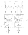
- FIG 1 a block diagram shows a telecommunications system according to the present invention.
- Figure 1 shows a block diagram of a telecommunications system of the SDH type wherein the signal is transmitted over a coaxial cable 20.
- An input signal SI containing SDH frames is transmitted over said coaxial cable 20, i.e. a lossy medium and reaches the input of a conversion interface 10 comprising a reception channel 11 and a transmission channel 15.
- the input signal SI which is a 155 Mbit/s CMI signal, is received through the reception channel 11, in particular by an equalizer block 12, which is apt to compensate the distortion on the input signal SI induced by the coaxial cable 20.
- the equalizer block 12 also comprises a signal loss detector, which is apt to detect the lack of transitions of the input signal SI for a certain number of cycles.
- the equalizer block 12 provides at its output an equalized signal SIE, which is still a CMI signal, but with a compensated distortion adapted to specific requests.
- Said equalized signal SIE is then sent to a recovery and conversion block 13, which comprises a first clock recovery stage 13b, consisting essentially of a phase locked loop obtained through a DLL (Delay Line Loop) circuit and operating at 155 MHz operational frequency, which will re-clock the data flow contained in the equalized signal SIE.
- a recovery and conversion block 13 which comprises a first clock recovery stage 13b, consisting essentially of a phase locked loop obtained through a DLL (Delay Line Loop) circuit and operating at 155 MHz operational frequency, which will re-clock the data flow contained in the equalized signal SIE.
- DLL Delay Line Loop
- a second conversion stage 13a consisting of a CMI/NRZ decoder, performs data conversion in a decoded signal SIEC, which is NRZ type.
- an input clock signal ICK which is the clock signal recovered through the first recovery stage 13b, is supplied at the output of the recovery and conversion block 13.
- the reception channel 11 comprises a shift block 14. Said shift block 14 converts both the decoded signal SIEC and the input clock signal ICK in a received data signal RXD and a received clock signal RXC, respectively, which are Low Voltage Differential Signals.
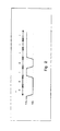
- Figure 2 represents an example of a received data signal RXD, which is measured between two terminals A and B, not shown in the figures.
- the logic signal is worth zero when the voltage VA on terminal A is higher than the voltage VB on terminal B, and it takes the value one if the voltage VB on terminal B is higher than the voltage on the terminal A.
- the maximum high value for voltages VA or VB is for instance 1.475 V, whereas the minimum low voltage is 0.9 V.
- the received data signal RXD as LVDS signal, is a differential signal with 1.2 V offset and 400 mV swing.
- the received data signal RXD and received clock signal RXC are the outputs of the conversion interface 10 and are sent to a signal processing station 19, which may typically be, for instance, a switch matrix performing its function of making connections, which re-allocates the position of the Virtual Containers inside SDH frames contained in the input signal SI, and exiting a signal SU containing re-processed SDH frames.
- a signal processing station 19 may typically be, for instance, a switch matrix performing its function of making connections, which re-allocates the position of the Virtual Containers inside SDH frames contained in the input signal SI, and exiting a signal SU containing re-processed SDH frames.
- the signal processing station 19 of the telecommunications systems comprises an input buffer 21 for the received data signal RXD, and a clock input buffer 22 for the received clock signal RXC.
- Said input buffer 21 and clock input buffer 22 are obtained through circuits operating according to LVDS voltage levels and corresponding circuitry technologies, so as to ensure enough speed to operate with 155 MHz signals, though maintaining a low consumption.
- Said input buffer 21 and clock input buffer 22 will then send received data signals RTD and received clock signals RTC to be handled to a matrix block 25, which is substantially the ASIC circuit according to CMOS technology featuring the switch matrix. Consequently, the received data signals RTD to be handled and received clock signals RTC to be handled will have levels suitable for CMOS technology.
- a transmitted handled data signal TTD and a transmitted handled clock signal TTC with CMOS levels associated, which are converted by their respective data output buffer 23 and clock output buffer 24 in LVDS signals, namely, the signal processing station 19 will send to the transmission channel 15 of the conversion interface 10 a transmitted data signal TXD and a transmitted clock signal TXC, which are NRZ signals identified by LVDS logic levels.
- the transmission channel 15 provides a shift block 18 operating conversion of the transmitted data signal TXD in a converted data output signal SSU and conversion of the transmitted clock signal in an output clock signal OCK, which have the logic levels of the signal apt for cable transmission, i.e. between - 0.6 V and 0.6 V.
- a conversion and synchronization block 17 located downstream comprises a first conversion stage 17a, which performs the coding of the converted data output signal SSU from NRZ signal to a CMI signal type, represented by a coded output signal CSU.
- a second synchronization stage 17b is obtained through a further circuit DLL and used to correct undesired 'skew' effects contained in the converted data output signal SSU and in the transmitted clock signal in an output clock signal OCK before its coding through the first conversion stage 17a.
- the coded output signal CSU is sent to a masking block 16, which shapes the signal in order to make it compatible with the specifications for transmission on the coaxial cable 20 and adapted for driving at a 75 Q impedance of the coaxial cables.
- the output signal SU containing re-processed SDH frames and sent on the coaxial cable 20 from the conversion interface 10 is a CMI signal again at 155 MHz frequency with 1.2 V amplitude.
- the telecommunications system according to the present invention allows advantageously to minimize interferences by adopting an input/output circuit based on LVDS technology identified by differential signals, which provide a high common mode rejection and at a low voltage.
- LVDS signals have the required switching speed to transceive high frequency flows, such as 155 Mbit/s flows, implying decidedly lower consumption, for example when compared to ECL differential technologies.
- nodes with input/output circuits based on LVDS technology also will advantageously lead to a lower node consumption.
- the telecommunications system according to the present invention uses an interface converting the signal in LVDS signal, that show particularly low consumption compared with the transceivers usually employed, since DLL circuits are used instead of analog PLL circuits to perform data resynchronization.
- the interface has advantageously an equalizer circuit compensating the distortions induced by the physical medium and in particular by the coaxial cable.
- the telecommunications system according to the present invention may also be easily extended to PDH plesiochronous networks without departing from the inventive spirit characterizing it.
- the telecommunications system according to the present invention may be extended to networks using optical fiber layers (SONET networks) operating their optoelectric conversion through an interface circuit that provides a conversion device such as a photodiode, and conditioning directly the electrical signal obtained according to LVDS levels to send it directly to the input/output buffers.
- SONET networks optical fiber layers
Landscapes
- Physics & Mathematics (AREA)
- Spectroscopy & Molecular Physics (AREA)
- Engineering & Computer Science (AREA)
- Computer Networks & Wireless Communication (AREA)
- Signal Processing (AREA)
- Dc Digital Transmission (AREA)
- Exchange Systems With Centralized Control (AREA)
Applications Claiming Priority (2)
| Application Number | Priority Date | Filing Date | Title |
|---|---|---|---|
| ITTO990457 | 1999-05-31 | ||
| IT1999TO000457 IT1308065B1 (it) | 1999-05-31 | 1999-05-31 | Sistema di telecomunicazioni |
Publications (2)
| Publication Number | Publication Date |
|---|---|
| EP1058433A2 true EP1058433A2 (de) | 2000-12-06 |
| EP1058433A3 EP1058433A3 (de) | 2003-11-26 |
Family
ID=11417853
Family Applications (1)
| Application Number | Title | Priority Date | Filing Date |
|---|---|---|---|
| EP00401501A Withdrawn EP1058433A3 (de) | 1999-05-31 | 2000-05-26 | Konversion zwischen CMI und NRZ |
Country Status (3)
| Country | Link |
|---|---|
| EP (1) | EP1058433A3 (de) |
| CA (1) | CA2308047A1 (de) |
| IT (1) | IT1308065B1 (de) |
Family Cites Families (4)
| Publication number | Priority date | Publication date | Assignee | Title |
|---|---|---|---|---|
| JP2550985B2 (ja) * | 1987-04-21 | 1996-11-06 | 日本電気株式会社 | Cmi符号復号器 |
| KR920005364B1 (ko) * | 1989-12-12 | 1992-07-02 | 한국전기통신공사 | Nrz/cmi(ii) 부호 변환장치 |
| US5189410A (en) * | 1989-12-28 | 1993-02-23 | Fujitsu Limited | Digital cross connect system |
| US5488641A (en) * | 1992-12-10 | 1996-01-30 | Northern Telecom Limited | Digital phase-locked loop circuit |
-
1999
- 1999-05-31 IT IT1999TO000457 patent/IT1308065B1/it active
-
2000
- 2000-05-11 CA CA 2308047 patent/CA2308047A1/en not_active Abandoned
- 2000-05-26 EP EP00401501A patent/EP1058433A3/de not_active Withdrawn
Also Published As
| Publication number | Publication date |
|---|---|
| EP1058433A3 (de) | 2003-11-26 |
| IT1308065B1 (it) | 2001-11-29 |
| CA2308047A1 (en) | 2000-11-30 |
| ITTO990457A1 (it) | 2000-12-01 |
Similar Documents
| Publication | Publication Date | Title |
|---|---|---|
| US6449318B1 (en) | Variable low frequency offset, differential, OOK, high-speed twisted pair communication | |
| US5200979A (en) | High speed telecommunication system using a novel line code | |
| US8582705B2 (en) | Serializer-deserializer circuit with multi-format and multi-data rate capability | |
| US7472318B2 (en) | System and method for determining on-chip bit error rate (BER) in a communication system | |
| US8090047B2 (en) | System and method for programmably adjusting gain and frequency response in a 10-gigabit ethernet/fibre channel system | |
| US5134633A (en) | Digital communications synchronization scheme | |
| US20040028164A1 (en) | System and method for data transition control in a multirate communication system | |
| US20150146766A1 (en) | Use of multi-level modulation signaling for short reach data communications | |
| US7266169B2 (en) | Phase interpolater and applications thereof | |
| US8270526B2 (en) | Communication system | |
| CA1212161A (en) | Ring communications system | |
| US7224951B1 (en) | PMA RX in coarse loop for high speed sampling | |
| US6667994B1 (en) | Multiplexing digital communication system | |
| US20090251190A1 (en) | System and method for generating two effective frequencies using a single clock | |
| JP2002084247A (ja) | 伝送方法および伝送システム並びに通信装置 | |
| US4524462A (en) | System for jointly transmitting high-frequency and low-frequency digital signals over a fiber-optical carrier | |
| EP1388939A1 (de) | System und Verfahren zur Durchführung von On-Chip-Synchronisierung mittels eines externen Signals | |
| EP1058433A2 (de) | Konversion zwischen CMI und NRZ | |
| US7426235B1 (en) | Method of adaptive equalization for high-speed NRZ and multi-level signal data communications | |
| EP1523118B1 (de) | Optische Paketübertragung | |
| US6519328B1 (en) | Variable low frequency offset, differential, OOK, high-speed twisted pair communication using telephone load coils | |
| US5309475A (en) | Data interchange network | |
| US7577171B2 (en) | Source centered clock supporting quad 10 GBPS serial interface | |
| JP2581395B2 (ja) | 無線デジタル伝送システム | |
| US20030123592A1 (en) | Clock and data recovery unit |
Legal Events
| Date | Code | Title | Description |
|---|---|---|---|
| PUAI | Public reference made under article 153(3) epc to a published international application that has entered the european phase |
Free format text: ORIGINAL CODE: 0009012 |
|
| AK | Designated contracting states |
Kind code of ref document: A2 Designated state(s): AT BE CH CY DE DK ES FI FR GB GR IE IT LI LU MC NL PT SE |
|
| AX | Request for extension of the european patent |
Free format text: AL;LT;LV;MK;RO;SI |
|
| PUAL | Search report despatched |
Free format text: ORIGINAL CODE: 0009013 |
|
| AK | Designated contracting states |
Kind code of ref document: A3 Designated state(s): AT BE CH CY DE DK ES FI FR GB GR IE IT LI LU MC NL PT SE |
|
| AX | Request for extension of the european patent |
Extension state: AL LT LV MK RO SI |
|
| 17P | Request for examination filed |
Effective date: 20040419 |
|
| 17Q | First examination report despatched |
Effective date: 20040526 |
|
| AKX | Designation fees paid |
Designated state(s): AT BE CH CY DE DK ES FI FR GB GR IE IT LI LU MC NL PT SE |
|
| STAA | Information on the status of an ep patent application or granted ep patent |
Free format text: STATUS: THE APPLICATION IS DEEMED TO BE WITHDRAWN |
|
| 18D | Application deemed to be withdrawn |
Effective date: 20041006 |