EP1058387A2 - System with adjustable ADC clock phase - Google Patents
System with adjustable ADC clock phase Download PDFInfo
- Publication number
- EP1058387A2 EP1058387A2 EP00401516A EP00401516A EP1058387A2 EP 1058387 A2 EP1058387 A2 EP 1058387A2 EP 00401516 A EP00401516 A EP 00401516A EP 00401516 A EP00401516 A EP 00401516A EP 1058387 A2 EP1058387 A2 EP 1058387A2
- Authority
- EP
- European Patent Office
- Prior art keywords
- analog
- digital
- digital converter
- clock
- set forth
- Prior art date
- Legal status (The legal status is an assumption and is not a legal conclusion. Google has not performed a legal analysis and makes no representation as to the accuracy of the status listed.)
- Granted
Links
Images


Classifications
-
- H—ELECTRICITY
- H03—ELECTRONIC CIRCUITRY
- H03M—CODING; DECODING; CODE CONVERSION IN GENERAL
- H03M1/00—Analogue/digital conversion; Digital/analogue conversion
- H03M1/06—Continuously compensating for, or preventing, undesired influence of physical parameters
- H03M1/08—Continuously compensating for, or preventing, undesired influence of physical parameters of noise
-
- H—ELECTRICITY
- H03—ELECTRONIC CIRCUITRY
- H03M—CODING; DECODING; CODE CONVERSION IN GENERAL
- H03M1/00—Analogue/digital conversion; Digital/analogue conversion
- H03M1/06—Continuously compensating for, or preventing, undesired influence of physical parameters
- H03M1/08—Continuously compensating for, or preventing, undesired influence of physical parameters of noise
- H03M1/0818—Continuously compensating for, or preventing, undesired influence of physical parameters of noise of clock feed-through
-
- H—ELECTRICITY
- H03—ELECTRONIC CIRCUITRY
- H03M—CODING; DECODING; CODE CONVERSION IN GENERAL
- H03M1/00—Analogue/digital conversion; Digital/analogue conversion
- H03M1/12—Analogue/digital converters
Definitions
- This invention relates to clocking analog to digital converters and more particularly phasing the clock signal to an analog to digital converter on an IC having a multiplicity of different clock signals.
- DSP's Digital processing integrated circuits
- ADC's analog to digital converters
- the DSP's will have a plurality of functional elements, with respective elements clocked at different frequencies, though the ADC's may be clocked at the same frequency.
- the relative proximity of respective ADC's to various of the functional elements may adversely affect the performance of the ADC. It is known that coupling of clocking signals from the functional elements or clock buses to the ADC either through the silicon substrate or via radiation will tend to degrade ADC performance, particularly if the ADC is operating near its maximum conversion rate.
- Examples of DSP's containing a multiplicity of ADC's are multistandard interface circuits which condition signals in differing formats for processing by a common circuit element.
- a particular example is a television signal interface which conditions signal from different sources for digital processing and display. This interface may simultaneously accept NTSC signals from a broadcast receiver tuner, component analog television signals from a satellite or cable box, digitally broadcast VSB (vestigial sideband) signal from a further tuner etc. Nominally all of the signals will be converted from analog to digital form at a common sample rate and applied to respective processing elements for application to a display circuit. In the case of the digital VSB signal the processing will include digital decompression.
- the various processing functions may be performed at different clocking rates.
- the ADC used to convert a signal of a particular format will be located in proximity of the processing element to which the converted signals applied.
- ADC performance will be more or less affected.
- Performance of respective ADC's on circuitry containing a plurality of processing elements, and a plurality of associated clock signals of differing frequencies is enhanced by generating ADC clocking signals of varying phase and selecting an optimum one of the clock phases for application to the ADC.
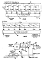
- Figure 1 is a block diagram of an interface circuit which includes a plurality of ADC's, and which is useful in describing the invention.
- Figure 2 is a waveform diagram illustrating exemplary clocking signals which may be employed in the Figure 1 circuitry.
- Figure 3 is a waveform diagram illustrating in part, analog to digital converter interference timing.
- Figure 4 is a waveform diagram illustrating in part, clock noise interference that multiple clocks may impose on analog to digital converters.
- Figure 5 is a waveform diagram of representative clock phases from which an optimum sampling clock phase may be selected
- Figures 6 and 7 are alternative exemplary sampling clock phase generating circuitry.
- Figure 8 is a block diagram of an analog to digital converter including a sampling clock phase generating circuit.
- Figure 1 is an interface integrated circuit which is useful in defining an environment of the invention, but is not restrictive.
- the invention may be practiced in any integrated circuit (IC) or other closely packed circuitry such as a multichip IC package or hybrid IC package incorporating analog to digital converters and where unpredictable noise interference may affect analog to digital performance.
- IC integrated circuit
- Other examples may include multiprocessor IC's for multimedia processing, multichannel digital audio processing/editing IC's and systems, just to name a couple.
- Figure 1 illustrates an interface or link IC for a multiplatform Television system.
- This IC is configured to simultaneously digitally process a plurality of television signals received in different formats.
- the respective processors are circumscribed with dashed lines.
- the circuitry circumscribed with dashed line 10 is configured to process digital direct broadcast satellite signal.
- This circuitry includes two analog to digital converters for processing quadrature signals from a satellite tuner, a digital demodulator and error correction circuitry. These elements may require different clocking signals such as for example, 18 MHz, 54 MHz and 27 MHz clock signals.
- a second processing block circumscribed by the dashed line 20 receives and processes high definition digital signals such as may be transmitted according to the Grand Alliance protocol.
- This circuitry includes at least one analog to digital converter, a digital demodulator, an equalizer/phase tracker and error correction circuitry. . These elements may require different clocking signals such as, for example, 108 MHz, 54 MHz and 18 MHz clock signals.
- the IC includes an NTSC signal processor circumscribed by the dashed line 30.
- This circuitry includes at least two analog to digital converters, filter circuitry, and digital color decoders. . These elements may require different clocking signals such as, for example, 18 MHz, 36 MHz and 27 MHz clock signals.
- the respective clocking signals will be provided by common clock generation circuitry including a phase locked loop to develop a master clock signal and a generator responsive to the master clock signal for providing a plurality of clock signals at different frequencies.
- the master clock is at 108 MHz
- the further clock signals are at 18, 27, 36 and 54 MHz.
- Figure 2 illustrates exemplary timing relationships of these clock signals. These particular clock signals are phase locked to each other and are all simple multiples of 9 MHz. It will be appreciated that a plurality of clock signals widely divergent from those illustrated may be employed in similar or different IC's, and to which the invention will apply.
- the respective analog to digital converters will nominally be adjacent to its associated processing circuitry and thus susceptible to clock signal interference from its associated circuitry. Additionally, the respective analog to digital converters will be susceptible to clock signal interference coupled through the IC substrate and power interconnects. Each of the analog to digital converters, because of its relative location on the IC will likely be susceptible to differing clock interference, and which interference will be unpredictable.
- FIG 3 there are a top, a middle and a bottom waveform.
- the top waveform is intended to indicate a clock signal in the vicinity of an analog to digital converter which processes samples at the same frequency as clock signal.
- the middle waveform is intended to indicate interfering noise power incurred by an analog to digital converter from the clock signal represented by the top waveform.
- the illustrated noise power is only representational, and may take differing forms and amplitudes.
- the lower waveform represents the optimum sampling phase for the sampling clock signal applied to the converter.
- analog to digital converter sampling initiates on the positive going transition of the sampling clock, i.e. the bottom waveform, and continues until the negative going transition.
- the sampling phase is selected so no clock noise interference occurs during this entire interval.
- the optimum sampling phase that is shown was arbitrarily selected and is exemplary only, but one skilled in the art of analog to digital design will appreciate that sampling should occur after any interfering noise abates. Different types of analog to digital converters will respond differently regarding sampling clock phase and the occurrence of clock interference. However, for each type of analog to digital converter there will be an optimum clocking phase.
- the optimum sampling phase of a single analog to digital converter may be accurately predicted and generated.
- Exemplary clock waveforms and possible exemplary interfering clock noise of such a system is demonstrated in the waveforms of Figure 4.
- the waveform designated NOISE shows potential noise interference generated by the positive transitions of all of the clock signals shown in Figure 4. It will be appreciated that, on an integrated circuit, the interfering noise at any location will be different for the different sources depending on the clock signal coupling mechanism and the relative locations of the sources to the respective analog to digital converter.
- the waveform immediately below the noise waveform illustrates a possible optimum sampling clock waveform, the phase of which, relative to the other clock signals, is uncertain.
- FIG. 6 shows circuitry for developing various sampling clock phases which lag in equal increments and are synchronous with a master clock.
- a sampling clock is applied to the input of a tapped delay line or shift register 40, which may comprise a cascade connection of D-type (or other type .e.g. RS) flip flops.
- the register 40 is clocked by a master clock signal of frequency higher than the sampling clock frequency.
- the sampling clock appears at the respective taps successively delayed by intervals defined by the frequency f c of the master clock F C , i.e. by increments of 1/f c .
- Figure 5 illustrates a plurality of possible sampling clock output phases derived from the Figure 6 system.
- the number and increments of the sampling clock phases are a matter of design choice.
- the output taps of register 40 are applied to input connections of a N+1-to-1 multiplexer 42.
- the multiplexer 42 couples signal from one of the taps to its output connection responsive to control signals applied to its control input C.
- the control signal may be user generated or it may be generated via an auto calibration algorithm as indicated above.
- FIG. 7 is a block diagram of alternative circuitry for generating successively delayed sampling clock phases.
- This circuit comprises a tapped analog delay line 50 of cascade connected analog delay circuits such as amplifiers (or they may be inverter circuits).
- the delay provided by respective amplifiers may be relatively short (in the order of nanoseconds) and corresponds to the inherent delay of the amplifier.
- sampling clock phases may be generated with a relatively fine vernier.
- the respective delays may also be generated with relatively longer intervals with appropriate choice of circuit elements.
- the delay line taps are coupled to the input connections of a M+1-to-1 multiplexer 52.
- the multiplexer 52 couples signal from one of the taps to its output connection responsive to control signals applied to its control input C.
- the control signal may be user generated or it may be generated via an auto calibration algorithm as indicated above.
- the input of the analog phase shift circuit (50, 52) may be coupled to the output of the digital phase shift circuit (40, 42) and the output sampling clock signal taken from the analog multiplexer 52. Coarse phase adjustment is performed in the digital shifter (40, 42) and fine phase adjustment may be performed in the analog shifter (50, 52).
- clock phase adjusting circuits using delay lines and multiplexers, or counters and logic devices, or programmable logic array devices etc. Selection of the particular type will primarily depend on the IC fabrication technology and designer preference.
- FIG 8 illustrates an ADC system including an analog to digital converter 80 which has its sampling clock phase developed by a phase shifter 85, which may be configured as either the Figure 6 or 7 circuits for example.
- the phase shifter 85 is responsive to an 18 MHz logic clock signal and develops the sampling clock therefrom.
- the digital output from the analog to digital converter 80 is directly coupled to a first input of a multiplexer 82 and to a second input of the multiplexer via a D-type flip flop.
- the output of the multiplexer is applied to a further D-type flip flop 83 for purposes of synchronization to the logic clock.
- the flip flop 83 is clocked by the 18 MHz clock signal
- the flip flop 81 is clocked by the complement of the 18 MHz clock signal.
- the multiplexer is statically controlled by a control signal delay_ADC_output, which may be provided on an I2C bus.
- the flip flop 81 and the multiplexer 82 form a clock transfer circuit. This circuitry may be necessary by virtue of using a relatively large phase shifted sampling signal.
- the delay_ADC_control signal sets the multiplexer to couple its output to the analog to digital converter via the flip flop 81. This provides a half cycle of timing margin between the analog to digital converter output and the 18 MHz logic.
- the delay_ADC_control signal conditions the multiplexer to couple its output directly to the analog to digital converter, as there is no significant timing misalignment.
- the multiplexer delay_ADC_output control signal will be established concurrently with the sampling clock phase selection and will remain relatively static, unless the sampling phase selection is changing dynamically. In the latter case, the delay_ADC_output control signal must also be altered dynamically.
Landscapes
- Engineering & Computer Science (AREA)
- Theoretical Computer Science (AREA)
- Analogue/Digital Conversion (AREA)
- Stabilization Of Oscillater, Synchronisation, Frequency Synthesizers (AREA)
Abstract
Description
Claims (11)
- In digital circuit apparatus including an analog to digital converter (80), and processing circuitry (10; 20; 30) responsive to clocking signals, further apparatus for deriving a clock signal for operating said analog to digital converter, characterized by:a source of a clock signal;phase control circuitry (85)coupled to said source for providing a clock signal of selected phase; andmeans for connecting said clock signal of selected phase (85) to operate said analog to digital converter (80).
- The further apparatus set forth in claim 1 further characterized by:a delay register coupled to receive digital samples from said analog to digital converter; anda selector switch for selecting digital samples from said analog to digital converter, or delayed samples from the delay register coupled to said analog to digital converter
- In an integrated circuit containing a plurality of analog to digital converters (80), a plurality of processor circuits (10; 20; 30) coupled to output terminals of respective said converters and interconnections for a plurality of different frequency clock signals, further apparatus for deriving a clock signal for operating at least one of said analog to digital converters, characterized by:a source of an analog to digital clock signal;phase control circuitry (85) coupled to said source for providing a clock signal of selected phase; andmeans for connecting said clock signal of selected phase (85) to operate said analog to digital converter (80).
- The further apparatus set forth in claim 1 or 3 characterized in that said phase control circuitry includes:a serial input-parallel output delay line connected to said source and having a plurality output terminals, each successive output terminal providing input signal with different timing phase; anda multiplexer having respective parallel input terminals connected to the parallel output terminals of said delay line, an output terminal connected to said analog to digital converter and a control input terminal.
- The further apparatus set forth in claim 1 or 3 characterized in that said multiplexer control terminal is coupled to an I2C bus for receiving control signals from a controller.
- The further apparatus set forth in claim 4 characterized in that said delay line is a clocked shift register.
- The further apparatus set forth in claim 4 characterized in that said delay line is an analog delay line.
- The further apparatus set forth in claim 4 characterized by clock phase control circuitry for each of said analog to digital converters.
- The further apparatus set forth in claim 4, further characterized by:a delay register coupled to receive digital samples from said at least one of said analog to digital converters; anda selector switch for selecting digital samples from said at least one of said analog to digital converters, or delayed samples from said delay register.
- The further apparatus set forth in claim 8 characterized in that for each analog to digital converter:a delay register is coupled to receive digital samples from each said analog to digital converter; anda selector switch is provided for selecting digital samples from respective said each analog to digital converter, or delayed samples from the delay register coupled to said analog to digital converter
- The further apparatus set forth in claim 2 or 10 characterized in that said selector switch is controlled by an I2C bus.
Priority Applications (1)
| Application Number | Priority Date | Filing Date | Title |
|---|---|---|---|
| EP06121705A EP1758252B1 (en) | 1999-06-04 | 2000-05-30 | Digital circuit apparatus with adjustable ADC clock phase |
Applications Claiming Priority (2)
| Application Number | Priority Date | Filing Date | Title |
|---|---|---|---|
| US09/327,088 US6310570B1 (en) | 1999-06-04 | 1999-06-04 | System with adjustable ADC clock phase |
| US327088 | 1999-06-04 |
Related Child Applications (1)
| Application Number | Title | Priority Date | Filing Date |
|---|---|---|---|
| EP06121705A Division EP1758252B1 (en) | 1999-06-04 | 2000-05-30 | Digital circuit apparatus with adjustable ADC clock phase |
Publications (3)
| Publication Number | Publication Date |
|---|---|
| EP1058387A2 true EP1058387A2 (en) | 2000-12-06 |
| EP1058387A3 EP1058387A3 (en) | 2003-10-29 |
| EP1058387B1 EP1058387B1 (en) | 2007-07-11 |
Family
ID=23275112
Family Applications (2)
| Application Number | Title | Priority Date | Filing Date |
|---|---|---|---|
| EP00401516A Expired - Lifetime EP1058387B1 (en) | 1999-06-04 | 2000-05-30 | System with adjustable ADC clock phase |
| EP06121705A Expired - Lifetime EP1758252B1 (en) | 1999-06-04 | 2000-05-30 | Digital circuit apparatus with adjustable ADC clock phase |
Family Applications After (1)
| Application Number | Title | Priority Date | Filing Date |
|---|---|---|---|
| EP06121705A Expired - Lifetime EP1758252B1 (en) | 1999-06-04 | 2000-05-30 | Digital circuit apparatus with adjustable ADC clock phase |
Country Status (9)
| Country | Link |
|---|---|
| US (1) | US6310570B1 (en) |
| EP (2) | EP1058387B1 (en) |
| JP (2) | JP2001053609A (en) |
| KR (1) | KR101054855B1 (en) |
| CN (2) | CN100361394C (en) |
| BR (1) | BR0002574A (en) |
| DE (2) | DE60035456T2 (en) |
| MX (1) | MXPA00005503A (en) |
| MY (1) | MY123664A (en) |
Cited By (1)
| Publication number | Priority date | Publication date | Assignee | Title |
|---|---|---|---|---|
| WO2006105323A1 (en) * | 2005-03-30 | 2006-10-05 | Silicon Laboratories, Inc. | Method and system for sampling a signal |
Families Citing this family (31)
| Publication number | Priority date | Publication date | Assignee | Title |
|---|---|---|---|---|
| US6420989B1 (en) * | 2001-01-22 | 2002-07-16 | Credence Systems Corporation | Programmable non-uniform clock signal generator |
| US7805628B2 (en) * | 2001-04-02 | 2010-09-28 | Credence Systems Corporation | High resolution clock signal generator |
| WO2002084937A1 (en) * | 2001-04-09 | 2002-10-24 | Matsushita Electric Industrial Co., Ltd. | Synchronization detection apparatus |
| US7224759B2 (en) * | 2002-07-11 | 2007-05-29 | Honeywell International Inc. | Methods and apparatus for delay free phase shifting in correcting PLL phase offset |
| EP1530841B1 (en) * | 2002-08-14 | 2020-01-08 | Standard Microsystems Corporation | Communication system for sending and receiving data onto and from a network at a network frame rate synchronizing clocks generated from the network frame rate |
| JP2004260669A (en) * | 2003-02-27 | 2004-09-16 | Leader Electronics Corp | Word clock generator that synchronizes to a timing reference bit string inherent in a serial digital signal |
| KR100538226B1 (en) * | 2003-07-18 | 2005-12-21 | 삼성전자주식회사 | Analog to digital converting device for processing plural analog input signal by high speed and display apparatus using the same |
| US20090072895A1 (en) * | 2005-06-14 | 2009-03-19 | Nxp B.V. | Signal processing with interference compensation |
| US8331512B2 (en) | 2006-04-04 | 2012-12-11 | Rambus Inc. | Phase control block for managing multiple clock domains in systems with frequency offsets |
| KR100835682B1 (en) * | 2006-07-18 | 2008-06-09 | 고려대학교 산학협력단 | Analog-to-digital converter for controlling sampling period according to noise, audio recording device and pacemaker |
| US7612595B2 (en) * | 2006-09-19 | 2009-11-03 | Melexis Tessenderlo Nv | Sequence independent non-overlapping digital signal generator with programmable delay |
| US7928884B2 (en) * | 2007-01-11 | 2011-04-19 | Siflare, Inc. | Analog-to-digital converter with a balanced output |
| US7940202B1 (en) * | 2008-07-31 | 2011-05-10 | Cypress Semiconductor Corporation | Clocking analog components operating in a digital system |
| EP2226963B1 (en) * | 2009-03-04 | 2013-05-08 | Sony Corporation | Receiving apparatus and method with non-oversampling analog to digital conversion |
| JP5221446B2 (en) | 2009-05-19 | 2013-06-26 | 株式会社東芝 | Interference canceler and communication device |
| US8279100B2 (en) * | 2010-09-30 | 2012-10-02 | Lockheed Martin Corporation | Complex analog to digital converter (CADC) system on chip double rate architecture |
| CN101977057B (en) * | 2010-11-04 | 2013-05-22 | 青岛海信移动通信技术股份有限公司 | An analog-to-digital conversion circuit |
| JP5547765B2 (en) * | 2012-03-23 | 2014-07-16 | 旭化成エレクトロニクス株式会社 | D / A converter, jitter frequency control circuit |
| JP5547767B2 (en) * | 2012-03-28 | 2014-07-16 | 旭化成エレクトロニクス株式会社 | Sampling circuit, A / D converter, D / A converter, CODEC |
| DE102012208281A1 (en) * | 2012-05-16 | 2013-11-21 | Robert Bosch Gmbh | Method for suppressing a scanning process and an apparatus for carrying out the method |
| US9000809B2 (en) * | 2012-05-30 | 2015-04-07 | Infineon Technologies Austria Ag | Method and device for sampling an input signal |
| CN104158542B (en) * | 2014-08-25 | 2017-04-05 | 东南大学 | It is a kind of that measuring circuit on piece is shaken based on Undersampling technique phaselocked loop long period |
| US9496887B1 (en) * | 2015-05-12 | 2016-11-15 | Microchip Technology Incorporated | Analog to digital converter with internal timer |
| US9312875B1 (en) * | 2015-06-26 | 2016-04-12 | Intel IP Corporation | Signal processing apparatus and method for processing a signal |
| CN108345554B (en) * | 2017-01-22 | 2020-08-21 | 联发科技股份有限公司 | Method for determining sampling phase of sampling clock signal and related electronic device |
| EP3591433B1 (en) * | 2018-07-02 | 2023-06-14 | NXP USA, Inc. | Communication unit, integrated circuits and method for clock and data synchronization |
| CN113237501B (en) * | 2021-04-19 | 2022-06-17 | 上海季丰电子股份有限公司 | High-precision multichannel signal calibration method and device |
| EP4089435B1 (en) | 2021-05-12 | 2025-05-28 | Nxp B.V. | Radar system |
| JP7799169B2 (en) * | 2021-11-24 | 2026-01-15 | 株式会社ソシオネクスト | Processing circuit, wireless communication circuit and semiconductor integrated circuit |
| CN114389607B (en) * | 2021-12-24 | 2024-06-04 | 莱弗利科技(苏州)有限公司 | Digital-analog hybrid chip with low noise interference |
| CN117411466A (en) * | 2023-11-07 | 2024-01-16 | 上海芯炽科技集团有限公司 | CDR circuit based on digital phase generator and selector |
Family Cites Families (13)
| Publication number | Priority date | Publication date | Assignee | Title |
|---|---|---|---|---|
| US4633226A (en) | 1984-12-17 | 1986-12-30 | Black Jr William C | Multiple channel analog-to-digital converters |
| US4791488A (en) * | 1987-08-12 | 1988-12-13 | Rca Licensing Corporation | Line-locked clock signal generation system |
| JP2805776B2 (en) * | 1988-11-18 | 1998-09-30 | 日本電気株式会社 | A / D converter |
| SE463584B (en) * | 1989-04-20 | 1990-12-10 | Ericsson Telefon Ab L M | SET AND DEVICE PROVIDES ANY DIGITAL SEATING OF THE TIME OR PHASES OF A SIGNAL PULSE TAG |
| JPH0375976A (en) * | 1989-08-18 | 1991-03-29 | Fujitsu Ltd | Semiconductor integrated circuit device |
| US5022056A (en) * | 1989-10-23 | 1991-06-04 | National Semiconductor Corporation | Method and structure for digital phase synchronization |
| US5319679A (en) * | 1992-12-09 | 1994-06-07 | Datum Systems | Method and apparatus for recovering data from a radio signal |
| US5533072A (en) * | 1993-11-12 | 1996-07-02 | International Business Machines Corporation | Digital phase alignment and integrated multichannel transceiver employing same |
| KR100322690B1 (en) * | 1994-06-30 | 2002-06-20 | 윤종용 | Digital Timing Restoration Circuit |
| US5596765A (en) * | 1994-10-19 | 1997-01-21 | Advanced Micro Devices, Inc. | Integrated processor including a device for multiplexing external pin signals |
| JP3622270B2 (en) * | 1995-06-16 | 2005-02-23 | セイコーエプソン株式会社 | Video signal processing apparatus, information processing system, and video signal processing method |
| JPH1049248A (en) * | 1996-07-29 | 1998-02-20 | Sharp Corp | Microcomputer |
| JPH10228733A (en) * | 1997-02-17 | 1998-08-25 | Matsushita Electric Ind Co Ltd | Data decoding device |
-
1999
- 1999-06-04 US US09/327,088 patent/US6310570B1/en not_active Expired - Lifetime
-
2000
- 2000-05-30 DE DE60035456T patent/DE60035456T2/en not_active Expired - Lifetime
- 2000-05-30 EP EP00401516A patent/EP1058387B1/en not_active Expired - Lifetime
- 2000-05-30 DE DE60044271T patent/DE60044271D1/en not_active Expired - Lifetime
- 2000-05-30 EP EP06121705A patent/EP1758252B1/en not_active Expired - Lifetime
- 2000-06-02 MX MXPA00005503A patent/MXPA00005503A/en active IP Right Grant
- 2000-06-02 BR BR0002574-7A patent/BR0002574A/en not_active Application Discontinuation
- 2000-06-02 MY MYPI20002485 patent/MY123664A/en unknown
- 2000-06-02 KR KR1020000030299A patent/KR101054855B1/en not_active Expired - Lifetime
- 2000-06-04 CN CNB2004100686690A patent/CN100361394C/en not_active Expired - Lifetime
- 2000-06-04 CN CNB001217038A patent/CN1187900C/en not_active Expired - Lifetime
- 2000-06-05 JP JP2000168139A patent/JP2001053609A/en active Pending
-
2011
- 2011-04-25 JP JP2011097513A patent/JP2011223589A/en active Pending
Cited By (3)
| Publication number | Priority date | Publication date | Assignee | Title |
|---|---|---|---|---|
| WO2006105323A1 (en) * | 2005-03-30 | 2006-10-05 | Silicon Laboratories, Inc. | Method and system for sampling a signal |
| US7209061B2 (en) | 2005-03-30 | 2007-04-24 | Silicon Laboratories, Inc. | Method and system for sampling a signal |
| US7424275B2 (en) | 2005-03-30 | 2008-09-09 | Silicon Laboratories, Inc. | Method and system for sampling a signal |
Also Published As
| Publication number | Publication date |
|---|---|
| DE60035456D1 (en) | 2007-08-23 |
| CN100361394C (en) | 2008-01-09 |
| MY123664A (en) | 2006-05-31 |
| KR20010007195A (en) | 2001-01-26 |
| CN1277492A (en) | 2000-12-20 |
| MXPA00005503A (en) | 2004-06-07 |
| JP2001053609A (en) | 2001-02-23 |
| HK1070756A1 (en) | 2005-06-24 |
| CN1187900C (en) | 2005-02-02 |
| EP1058387A3 (en) | 2003-10-29 |
| BR0002574A (en) | 2001-01-02 |
| EP1058387B1 (en) | 2007-07-11 |
| CN1578153A (en) | 2005-02-09 |
| EP1758252B1 (en) | 2010-04-21 |
| EP1758252A1 (en) | 2007-02-28 |
| JP2011223589A (en) | 2011-11-04 |
| DE60035456T2 (en) | 2008-03-13 |
| US6310570B1 (en) | 2001-10-30 |
| DE60044271D1 (en) | 2010-06-02 |
| KR101054855B1 (en) | 2011-08-05 |
Similar Documents
| Publication | Publication Date | Title |
|---|---|---|
| US6310570B1 (en) | System with adjustable ADC clock phase | |
| US8477056B2 (en) | Method, system, and apparatus for interpolating an output of an analog-to-digital converter | |
| JP3089104B2 (en) | Moving average filter and A / D converter using the same | |
| CN100527802C (en) | Multiplexed analog-to-digital converter arrangement | |
| GB2038138A (en) | Integrated circuit for a tv receiver | |
| US4901151A (en) | Television receiving section with digital stages | |
| US5548244A (en) | Method and apparatus for eliminating DC offset for digital I/Q demodulators | |
| CN108432140A (en) | A kind of means for correcting and method | |
| CA2468269A1 (en) | Phase-locked loop (pll) circuit for selectively correcting clock skew in different modes | |
| KR100711131B1 (en) | Data transfer apparatus for system having plural clock domains | |
| US4963817A (en) | Method and apparatus for detecting a phase difference between two digital signals | |
| US8565293B2 (en) | Method for synchronizing a plurality of measuring channel assemblies and/or measuring devices, and appropriate measuring device | |
| HK1070756B (en) | Apparatus with adjustable adc clock phase | |
| US7348914B1 (en) | Method and systems to align outputs signals of an analog-to-digital converter | |
| JP4741484B2 (en) | Self-aligned data path converter for multiple clock systems. | |
| US7471753B2 (en) | Serializer clock synthesizer | |
| US7482960B2 (en) | Arrangement for the synchronous output of analog signals generated in two or more digital-to-analog converters | |
| JP2561336B2 (en) | Television receiver with digital processing stage | |
| US20080062324A1 (en) | Chroma/Luma Delay Adjustment | |
| US7679541B2 (en) | Circuit and method for improving mismatches between signal converters | |
| JP2644682B2 (en) | Correlation processing circuit | |
| Glascott-Jones et al. | A Quad 12bit 1.6 GSps ADC with Synchronization feature for use in Multi-element Systems | |
| JPH04266281A (en) | Hardware configuration of digital filter for interpolation | |
| JPH01220555A (en) | Semiconductor integrated circuit | |
| JPH0591418A (en) | Phase compensating circuit |
Legal Events
| Date | Code | Title | Description |
|---|---|---|---|
| PUAI | Public reference made under article 153(3) epc to a published international application that has entered the european phase |
Free format text: ORIGINAL CODE: 0009012 |
|
| AK | Designated contracting states |
Kind code of ref document: A2 Designated state(s): AT BE CH CY DE DK ES FI FR GB GR IE IT LI LU MC NL PT SE |
|
| AX | Request for extension of the european patent |
Free format text: AL;LT;LV;MK;RO;SI |
|
| RAP1 | Party data changed (applicant data changed or rights of an application transferred) |
Owner name: THOMSON LICENSING S.A. |
|
| PUAL | Search report despatched |
Free format text: ORIGINAL CODE: 0009013 |
|
| AK | Designated contracting states |
Kind code of ref document: A3 Designated state(s): AT BE CH CY DE DK ES FI FR GB GR IE IT LI LU MC NL PT SE |
|
| AX | Request for extension of the european patent |
Extension state: AL LT LV MK RO SI |
|
| 17P | Request for examination filed |
Effective date: 20040401 |
|
| AKX | Designation fees paid |
Designated state(s): DE FR GB IT |
|
| 17Q | First examination report despatched |
Effective date: 20050607 |
|
| RAP1 | Party data changed (applicant data changed or rights of an application transferred) |
Owner name: THOMSON LICENSING |
|
| GRAP | Despatch of communication of intention to grant a patent |
Free format text: ORIGINAL CODE: EPIDOSNIGR1 |
|
| GRAS | Grant fee paid |
Free format text: ORIGINAL CODE: EPIDOSNIGR3 |
|
| GRAA | (expected) grant |
Free format text: ORIGINAL CODE: 0009210 |
|
| AK | Designated contracting states |
Kind code of ref document: B1 Designated state(s): DE FR GB IT |
|
| REG | Reference to a national code |
Ref country code: GB Ref legal event code: FG4D |
|
| REF | Corresponds to: |
Ref document number: 60035456 Country of ref document: DE Date of ref document: 20070823 Kind code of ref document: P |
|
| ET | Fr: translation filed | ||
| PLBE | No opposition filed within time limit |
Free format text: ORIGINAL CODE: 0009261 |
|
| STAA | Information on the status of an ep patent application or granted ep patent |
Free format text: STATUS: NO OPPOSITION FILED WITHIN TIME LIMIT |
|
| 26N | No opposition filed |
Effective date: 20080414 |
|
| PG25 | Lapsed in a contracting state [announced via postgrant information from national office to epo] |
Ref country code: IT Free format text: LAPSE BECAUSE OF NON-PAYMENT OF DUE FEES Effective date: 20080531 |
|
| REG | Reference to a national code |
Ref country code: FR Ref legal event code: PLFP Year of fee payment: 17 |
|
| REG | Reference to a national code |
Ref country code: FR Ref legal event code: PLFP Year of fee payment: 18 |
|
| REG | Reference to a national code |
Ref country code: DE Ref legal event code: R082 Ref document number: 60035456 Country of ref document: DE Representative=s name: DEHNS, DE Ref country code: DE Ref legal event code: R082 Ref document number: 60035456 Country of ref document: DE Representative=s name: HOFSTETTER, SCHURACK & PARTNER PATENT- UND REC, DE |
|
| REG | Reference to a national code |
Ref country code: GB Ref legal event code: 732E Free format text: REGISTERED BETWEEN 20170717 AND 20170719 |
|
| REG | Reference to a national code |
Ref country code: FR Ref legal event code: TP Owner name: THOMSON LICENSING DTV, FR Effective date: 20171030 |
|
| REG | Reference to a national code |
Ref country code: FR Ref legal event code: PLFP Year of fee payment: 19 |
|
| REG | Reference to a national code |
Ref country code: GB Ref legal event code: 732E Free format text: REGISTERED BETWEEN 20180927 AND 20181005 |
|
| REG | Reference to a national code |
Ref country code: DE Ref legal event code: R082 Ref document number: 60035456 Country of ref document: DE Representative=s name: DEHNS, DE Ref country code: DE Ref legal event code: R081 Ref document number: 60035456 Country of ref document: DE Owner name: INTERDIGITAL MADISON PATENT HOLDINGS, FR Free format text: FORMER OWNER: THOMSON LICENSING, BOULOGNE-BILLANCOURT, FR |
|
| PGFP | Annual fee paid to national office [announced via postgrant information from national office to epo] |
Ref country code: DE Payment date: 20190418 Year of fee payment: 20 |
|
| PGFP | Annual fee paid to national office [announced via postgrant information from national office to epo] |
Ref country code: FR Payment date: 20190419 Year of fee payment: 20 |
|
| PGFP | Annual fee paid to national office [announced via postgrant information from national office to epo] |
Ref country code: GB Payment date: 20190423 Year of fee payment: 20 |
|
| REG | Reference to a national code |
Ref country code: DE Ref legal event code: R071 Ref document number: 60035456 Country of ref document: DE |
|
| REG | Reference to a national code |
Ref country code: GB Ref legal event code: PE20 Expiry date: 20200529 |
|
| PG25 | Lapsed in a contracting state [announced via postgrant information from national office to epo] |
Ref country code: GB Free format text: LAPSE BECAUSE OF EXPIRATION OF PROTECTION Effective date: 20200529 |