EP1058319A2 - Method for stabilizing SOI semiconductor device and SOI semiconductor device - Google Patents
Method for stabilizing SOI semiconductor device and SOI semiconductor device Download PDFInfo
- Publication number
- EP1058319A2 EP1058319A2 EP00301233A EP00301233A EP1058319A2 EP 1058319 A2 EP1058319 A2 EP 1058319A2 EP 00301233 A EP00301233 A EP 00301233A EP 00301233 A EP00301233 A EP 00301233A EP 1058319 A2 EP1058319 A2 EP 1058319A2
- Authority
- EP
- European Patent Office
- Prior art keywords
- semiconductor device
- source
- insulating film
- semiconductor layer
- soi
- Prior art date
- Legal status (The legal status is an assumption and is not a legal conclusion. Google has not performed a legal analysis and makes no representation as to the accuracy of the status listed.)
- Withdrawn
Links
Images


Classifications
-
- H—ELECTRICITY
- H10—SEMICONDUCTOR DEVICES; ELECTRIC SOLID-STATE DEVICES NOT OTHERWISE PROVIDED FOR
- H10D—INORGANIC ELECTRIC SEMICONDUCTOR DEVICES
- H10D30/00—Field-effect transistors [FET]
- H10D30/60—Insulated-gate field-effect transistors [IGFET]
-
- H—ELECTRICITY
- H10—SEMICONDUCTOR DEVICES; ELECTRIC SOLID-STATE DEVICES NOT OTHERWISE PROVIDED FOR
- H10D—INORGANIC ELECTRIC SEMICONDUCTOR DEVICES
- H10D30/00—Field-effect transistors [FET]
- H10D30/60—Insulated-gate field-effect transistors [IGFET]
- H10D30/67—Thin-film transistors [TFT]
- H10D30/6729—Thin-film transistors [TFT] characterised by the electrodes
- H10D30/673—Thin-film transistors [TFT] characterised by the electrodes characterised by the shapes, relative sizes or dispositions of the gate electrodes
- H10D30/6733—Multi-gate TFTs
- H10D30/6734—Multi-gate TFTs having gate electrodes arranged on both top and bottom sides of the channel, e.g. dual-gate TFTs
-
- H—ELECTRICITY
- H10—SEMICONDUCTOR DEVICES; ELECTRIC SOLID-STATE DEVICES NOT OTHERWISE PROVIDED FOR
- H10D—INORGANIC ELECTRIC SEMICONDUCTOR DEVICES
- H10D30/00—Field-effect transistors [FET]
- H10D30/60—Insulated-gate field-effect transistors [IGFET]
- H10D30/67—Thin-film transistors [TFT]
- H10D30/6757—Thin-film transistors [TFT] characterised by the structure of the channel, e.g. transverse or longitudinal shape or doping profile
Definitions
- the present invention relates to a method for stabilizing a semiconductor device of SOI (Semiconductor On Insulator) structure and an SOI semiconductor device stabilized by the method.
- SOI semiconductor On Insulator
- a positive voltage is applied to a drain 4. Accordingly, electrons are drawn from a source 5 and travel to the drain 4 via a channel 11. At this time, the electrons travel through the fine channel 11 of SOI-NMOSFET into the vicinity of the drain where an electric field strength is high, thereby turning to a high energy state. Then the electrons arrived at the drain 4 bring about an impact ionization and generate electron-hole pairs. The electrons newly generated by the impact ionization flow into the drain 4, while holes 12 gather at a lower portion of a surface silicon layer 3 adjacent to the source 5, where potential is low.
- FIG. 11 A model of a leak current in this stand-by state is shown in an equivalent circuit of Fig. 11. According to Fig. 11, a floating body effect by the impact ionization can be mentioned as a main factor dominant over an off-leak current.
- the electrons discharged from the source 5 become a current Ich.
- the electrons bring about the impact ionization with a certain probability in the vicinity of the drain 4 and are multiplied by a multiplication coefficient (M-1), thereby turning to a current Ii (a current caused by the electrons generated by the impact ionization).
- M-1 multiplication coefficient
- the holes discharged from the drain 4 accumulate at a body 13 (a lower portion of the surface silicon layer).
- the holes 12 accumulated at the body 13 raise a substrate potential Vbs, i.e., cause the floating body effect.
- a parasitic bipolar effect increases. That is, in an NMOSFET, an NPN type bipolar structure is formed from the source/drain regions and the body 13 lying therebetween. Accordingly, the rise in the body potential causes the electrons to be easily taken out from the source 5, thereby increasing a current Ic flowing into the drain via the body or base of the NPN bipolar transistor. The current Ic flows together with the current Ich and further increase the impact ionization. Thus, the parasitic bipolar effect becomes a factor for a positive feedback with respect to the off-leak current (in Fig. 11, a current Ib is a current caused by the holes generated by the impact ionization and the parasitic bipolar effect, and ⁇ is the current gain of the parasitic bipolar effect).
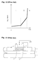
- the off-leak current of the MOSFET shows a behavior as shown in Fig. 12.
- the increase in the voltage Vbs and back bias effect become the dominant factor of the leak current.
- the parasitic bipolar effect may be increased and the impact ionization may be generated, which increases further the leakage current (the region II).
- the crystal defect is formed in a surface silicon layer of a substrate having the SOI structure, thereby reducing a carrier mobility and a drive current of a transistor. Further, this method is problematic in terms of industrial application because it causes multiplication of fabrication processes and an increase in product costs.
- a technique which is attempted to introduce the capturing potential by utilizing an electric stress has been proposed (Japanese Unexamined Patent Publication No. HEI 9 (1997)-8259).
- a support substrate 1 is maintained at a temperature of 100 to 200°C
- a gate 6, a drain 4 and a source 5 are grounded and a positive voltage is applied to the support substrate 1.
- a defect 8 can be caused to be introduced to a channel region 7 by the electric stress.
- the defect 8 serves as the capturing potential of carriers and results in the reduction of the leak current in the stand-by state.
- the formation of the defect by the electric stress is checked by a charge bombing method.
- the substrate must be heated up to around 200°C and the electric stress is applied for several hours. Therefore it is inefficient and difficult to realize industrially. Further, the electric stress is also applied to the front channel region 9. So the defect are formed front channel region 9. Accordingly, the drive current of the transistor may possibly be lowered.
- a method for stabilizing an SOI semiconductor device which comprises the steps of: providing an SOI semiconductor device constituted of an SOI substrate including a support substrate, a buried insulating film formed on the support substrate and a surface semiconductor layer formed on the buried insulating film, source/drain regions formed in the surface semiconductor layer and a gate electrode formed on the surface semiconductor layer between the source/drain regions with intervention of a gate insulating film; and applying an electric stress between the support substrate and one of the source/drain regions so that a back channel is formed in a side of the surface semiconductor layer to the buried insulating film, thereby to introduce a capturing potential at least near an interface between said one of the source/drain regions and the surface semiconductor layer in the buried insulating film side.
- the present invention provides an SOI semiconductor device stabilized by the above method.
- the present invention has been achieved by developing a method for applying the electric stress based on a principle drastically different from that of the conventional techniques in view of the above problems.
- the present invention provides an effective method for stabilizing an SOI semiconductor device in which the capturing potential is introduced only to a suitable position in a short time (several seconds to several hundred seconds) without raising the substrate temperature, and a semiconductor device obtained by the method.
- An SOI semiconductor device used in the method for stabilizing the SOI semiconductor device of the present invention is mainly constituted of an SOI substrate in which a buried insulating film and a surface semiconductor layer are laminated in this order on a support substrate, source/drain regions formed in the surface semiconductor layer of the SOI substrate and a gate electrode formed on the surface semiconductor layer between the source/drain regions with the intervention of a gate insulating film.
- the SOI substrate is not particularly limited as long as it is formed of a material, in a structure and thickness ordinarily used.
- BESOI and SIMOX (Separation by Implantation of Oxygen) semiconductor substrates are mentioned.
- the support substrate various kinds of substrates are used, for example, semiconductor substrates of silicon, germanium and the like, compound semiconductor substrates of GaAs, InGaAs and the like, insulative substrates of sapphire, quartz, glass, plastic and the like.
- the buried insulating film may be, for example, an SiO 2 film or an SiN film.
- the thickness of the buried insulating film can be appropriately adjusted in view of the characteristics of an intended semiconductor device, the magnitude of a voltage to be applied to an obtained semiconductor device for use and the like, but may be about 50 to 500 nm, for example.
- the surface semiconductor layer is a thin semiconductor layer which serves as an active layer for forming a transistor and can be formed of a thin film of a semiconductor such as silicon or germanium, or a compound semiconductor such as GaAs or InGaAs. Among them, a thin film of silicon is preferable.
- the thickness of the surface semiconductor layer can be appropriately adjusted to about 30 to 200nm depending on, for example, various parameters such as a junction depth of source/drain regions of a transistor, a depth of a channel region formed on a surface of the surface semiconductor layer and impurity concentration. These parameters will be explained later. Further, the surface semiconductor layer is provided with the source/drain regions and the channel region as described later.
- the impurity concentration for example, N-type impurities such as phosphorus or arsenic, or P-type impurities such as boron
- the concentration corresponds to a threshold value of the semiconductor device to be obtained.
- the source/drain regions formed in the surface semiconductor layer are preferably formed to have a junction depth equal to the thickness of the surface semiconductor layer.
- An impurity in the source/drain regions is not particularly limited to any type and may be of N-type or of P-type. Also an impurity concentration is not particularly limited. For example, an N-type impurity may be contained in an amount of about 1 ⁇ 10 20 to 1 ⁇ 10 21 atoms/cm 3 . Further, the source/drain regions may have an LDD structure.
- the gate insulating film and the gate electrode formed on the surface semiconductor layer between the source/drain regions are not particularly limited as long as they are made of a material in a thickness commonly employed for a semiconductor device.
- the gate insulating film can be made of a silicon oxide film, a silicon nitride film or a laminated film thereof in a thickness of about 3 to 10nm.
- the gate electrode can be made of polysilicon; silicides of refractory metals such as W, Ta, Ti and Mo; polycides comprised of these silicides (for example, MoSi 2 and WSI 2 ) and polysilicon; and other metals in a thickness of about 150 to 300nm.
- the gate electrode may have sidewall spacers of an insulating film, taking a lateral diffusion of the impurity for forming the source/drain regions into consideration.
- an electric stress is applied between the support substrate and one of the source/drain regions.
- a voltage of about 1 to 5V (2.5 to 3.5V) and a voltage of about 5 to 20V are applied to the source and the substrate, respectively.
- a voltage of about 1 to 5V (2.5 to 3.5V) and a voltage of about 5 to 20V are applied to the drain and the substrate, respectively.
- a voltage of about -0.1 V to about -0.8, i.e., about -0.5V is applied to the gate for maintaining the surface in a slightly accumulated state so that a surface channel is not formed.
- a voltage of about 2.5 to 3.5V and a voltage of about -5 to -20V are applied to the source and the substrate, respectively.
- a voltage of about 2.5 to 3.5 V and a voltage of about -5 to -20V are applied to the drain and the substrate, respectively.
- a voltage of about 0.1 V to about 0.8, i.e., about 0.5V is applied to the gate so as to avoid the formation of a surface channel.
- the substrate temperature is preferably close to room temperature (about 30°C). In the method of the present invention, however, it is not necessary to control rigidly the substrate temperature since the application of the electric stress in the method of the present invention does not involve an increase in the substrate temperature.
- the electric stress is applied for about several seconds to several hundred seconds, particularly about 10 seconds to 500 seconds.
- the above-described voltage application for the above-described period of time may be conducted once or plural times, or voltage application may be done with changing the pattern of the above-described voltage applications. In view of simplification of the operation, it is preferable to conduct only one application of a desired voltage for a desired period of time.
- a back channel can be formed on a side of the surface semiconductor layer to the buried insulating film, with the surface semiconductor layer, the buried insulating film and the support substrate regarded as an active layer, a gate insulating film and a gate electrode, respectively.
- a capturing potential is introduced at least in the vicinity of an interface between one of the source/drain regions and the surface semiconductor layer on the buried insulating film side.
- the capturing potential may be introduced to the entire surface of the surface semiconductor layer on its buried insulating film side.
- the leak current in the stand-by state can be reduced because the capturing potential is introduced only in a desired position by the above method. Further, by a single application of the electric stress, the leak current in both of the forward and backward directions can be also reduced.
- an NMOSFET comprises an SOI substrate including a silicon substrate 1, a buried insulating film 2 of about 1000 ⁇ thick and a surface silicon layer 3 of about 577 ⁇ thick formed on the silicon substrate 1, a drain 4 and a source 5 formed in the surface silicon layer 3, and a gate electrode 6 formed on the surface silicon layer 3 with the intervention of a gate insulating film.
- the drain 4 of the NMOSFET was grounded and voltages of 2.5V and 5.0V were applied to the source 5 and the substrate 1, respectively.
- a period of applying a stress was set to 1 to 300 seconds.
- a substrate temperature at this time was about 20 to 30°C.
- a back channel 7 was formed in a side of the surface semiconductor layer 3 to the buried insulating film 2.
- a capturing potential 8 was introduced near an interface between the source 5 and the surface semiconductor layer 3 in the buried insulating film side.
- Fig. 4 shows a relationship of an off-leak current to a voltage Vds applied between the drain and the source under a forward biased state in a semiconductor device in which the electric stress was applied for 10, 20, 30, 120 and 300 seconds.
- the leak current in regions I and II shows a decrease as illustrated in Fig. 12. In particular, the decrease in the leak current in the region II is remarkable.
- Fig. 5 shows a relationship of the off-leak current to the voltage Vds applied between the drain and the source under a backward biased state in a semiconductor device in which the electric stress was applied for 20, 30, 120 and 300 seconds. As the period of time of applying the electric stress increases, reduction of the leak current similar to the results shown in Fig. 4 is observed.
- Figs. 6 and 7 show the relationship between the leak current and the application period of the electric stress in the cases where the forward and backward bias voltages are applied, respectively.
- Figs. 6 and 7 show that the reduction of the leak current is observed with the increase in the application period of the electric stress in both the cases of the forward and backward biased states, respectively.
- a body potential is usually raised by impact ionization caused by a voltage applied between the drain and the source in the stand-by state (a gate voltage is zero).
- a gate voltage is zero
- electrons are injected from the source 5 to the drain 4 (a bipolar effect).
- the electric stress is applied as described above and the capturing potential 8 is introduced to a lower portion of an interface between the source 5 and the surface silicon layer 2.
- the capturing potential 8 serves as a positive fixed charge and captures the injected electrons, thereby reducing the number of the effective injected electrons. Whether a positive voltage is applied to the drain or the source, the electrons are captured in both the cases by this phenomenon. Therefore, the leak current can be effectively reduced by a single application of the electric stress as in the present invention, even if a bidirectional voltage is applied to an actual circuit.
- the leak current in the stand-by state can be reduced in a simple method because it is not necessary to heat the substrate at the application of the electric stress.
- a semiconductor device which comprises an SOI substrate including a support substrate, a buried insulating film, and a surface semiconductor layer having source/drain regions formed therein, the buried insulating film and the surface semiconductor layer being formed on the support substrate, and a gate electrode formed on the surface semiconductor layer between the source/drain regions with the intervention of a gate insulating film, an electric stress is applied between the support substrate and one of the source/drain regions to form a back channel in a side of the surface semiconductor layer to the buried insulating film.
- a capturing potential is introduced at least near an interface between said one of the source/drain regions and the surface semiconductor layer in the buried insulating film side. Accordingly, the parasitic bipolar effect is supressed, decrease in the threshold voltage and the impact ionization are suppressed, and the leak current in the stand-by state is reduced without decreasing the drive current by a simple, easy and practical method.
Landscapes
- Thin Film Transistor (AREA)
Abstract
Description
Claims (12)
- A method for stabilizing an SOI semiconductor device which comprises the steps of:providing an SOI semiconductor device constituted of an SOI substrate including a support substrate, a buried insulating film formed on the support substrate and a surface semiconductor layer formed on the buried insulating film, source/drain regions formed in the surface semiconductor layer and a gate electrode formed on the surface semiconductor layer between the source/drain regions with intervention of a gate insulating film; andapplying an electric stress between the support substrate and one of the source/drain regions so that a back channel is formed in a side of the surface semiconductor layer to the buried insulating film, thereby to introduce a capturing potential at least near an interface between said one of the source/drain regions and the surface semiconductor layer in the buried insulating film side.
- The method according to claim 1, wherein a period of time of applying the electric stress is adjusted so that the capturing potential is introduced to the entire buried insulating film side of the surface semiconductor layer.
- The method according to claim 1 or 2, wherein the electric stress is applied by setting one of the source/drain regions at a ground potential and the other at a positive potential.
- The method according to claim 3, wherein the positive potential is 1 V to 5 V.
- The method according to claim 3, wherein the electric stress is applied by further setting the support substrate at a positive potential in the case of an N channel semiconductor device or at a negative potential in the case of an P channel semiconductor device.
- The method according to claim 5, wherein the positive potential is 5 V to 20 V and the negative potential is -5 V to -20 V.
- The method according to claim 3 or 5, wherein the electric stress is applied by further setting the gate electrode at a negative potential in the case of an N channel semiconductor device or at a positive potential in the case of an P channel semiconductor device so that a surface channel is not formed.
- The method according to claim 5, wherein the negative potential is -0.1 V to -0.8 V and the positive potential is 0.1 V to 0.8 V.
- The method according to claim 1, wherein the electric stress is applied for about several seconds to several hundred seconds.
- The method according to claim 9, wherein the electric stress is applied for about 10 seconds to 500 seconds.
- An SOI semiconductor device stabilized by the method according to claim 1.
- The SOI semiconductor device according to claim 5, wherein the electric stress is applied so that a unidirectional back channel is formed and a bidirectional leak current is reduced.
Applications Claiming Priority (2)
| Application Number | Priority Date | Filing Date | Title |
|---|---|---|---|
| JP15212499 | 1999-05-31 | ||
| JP15212499A JP3454752B2 (en) | 1999-05-31 | 1999-05-31 | SOI semiconductor device stabilization method and SOI semiconductor device |
Publications (2)
| Publication Number | Publication Date |
|---|---|
| EP1058319A2 true EP1058319A2 (en) | 2000-12-06 |
| EP1058319A3 EP1058319A3 (en) | 2002-07-31 |
Family
ID=15533597
Family Applications (1)
| Application Number | Title | Priority Date | Filing Date |
|---|---|---|---|
| EP00301233A Withdrawn EP1058319A3 (en) | 1999-05-31 | 2000-02-17 | Method for stabilizing SOI semiconductor device and SOI semiconductor device |
Country Status (6)
| Country | Link |
|---|---|
| US (1) | US6194282B1 (en) |
| EP (1) | EP1058319A3 (en) |
| JP (1) | JP3454752B2 (en) |
| KR (1) | KR100368030B1 (en) |
| CN (1) | CN1154191C (en) |
| TW (1) | TW492190B (en) |
Families Citing this family (6)
| Publication number | Priority date | Publication date | Assignee | Title |
|---|---|---|---|---|
| KR100387122B1 (en) * | 2000-09-15 | 2003-06-12 | 피티플러스(주) | Fabrication Method of Poly-Si Thin Film Transistor Having Back Bias Effects |
| US6969618B2 (en) * | 2002-08-23 | 2005-11-29 | Micron Technology, Inc. | SOI device having increased reliability and reduced free floating body effects |
| FR2860341B1 (en) * | 2003-09-26 | 2005-12-30 | Soitec Silicon On Insulator | METHOD FOR MANUFACTURING LOWERED LOWER MULTILAYER STRUCTURE |
| US7166876B2 (en) * | 2004-04-28 | 2007-01-23 | Taiwan Semiconductor Manufacturing Company, Ltd. | MOSFET with electrostatic discharge protection structure and method of fabrication |
| JP4316558B2 (en) * | 2005-06-28 | 2009-08-19 | 三星モバイルディスプレイ株式會社 | Organic light emitting display |
| US11023955B1 (en) | 2019-09-27 | 2021-06-01 | Valyant AI, Inc. | Outside ordering system |
Family Cites Families (3)
| Publication number | Priority date | Publication date | Assignee | Title |
|---|---|---|---|---|
| JPS6129175A (en) * | 1984-07-19 | 1986-02-10 | Toshiba Corp | Semiconductor device and manufacture thereof |
| EP0564204A3 (en) * | 1992-03-30 | 1994-09-28 | Mitsubishi Electric Corp | Semiconductor device |
| JP3284499B2 (en) * | 1995-06-14 | 2002-05-20 | 日本電信電話株式会社 | Method and apparatus for stabilizing characteristics of MOS integrated circuit |
-
1999
- 1999-05-31 JP JP15212499A patent/JP3454752B2/en not_active Expired - Fee Related
-
2000
- 2000-02-16 TW TW089102604A patent/TW492190B/en not_active IP Right Cessation
- 2000-02-17 EP EP00301233A patent/EP1058319A3/en not_active Withdrawn
- 2000-02-23 US US09/511,116 patent/US6194282B1/en not_active Expired - Lifetime
- 2000-03-31 CN CNB001053736A patent/CN1154191C/en not_active Expired - Fee Related
- 2000-05-16 KR KR10-2000-0026189A patent/KR100368030B1/en not_active Expired - Fee Related
Also Published As
| Publication number | Publication date |
|---|---|
| US6194282B1 (en) | 2001-02-27 |
| JP2000340797A (en) | 2000-12-08 |
| KR20010014918A (en) | 2001-02-26 |
| TW492190B (en) | 2002-06-21 |
| JP3454752B2 (en) | 2003-10-06 |
| CN1275810A (en) | 2000-12-06 |
| CN1154191C (en) | 2004-06-16 |
| EP1058319A3 (en) | 2002-07-31 |
| KR100368030B1 (en) | 2003-01-15 |
Similar Documents
| Publication | Publication Date | Title |
|---|---|---|
| US6452232B1 (en) | Semiconductor device having SOI structure and manufacturing method thereof | |
| US6407427B1 (en) | SOI wafer device and a method of fabricating the same | |
| KR100418643B1 (en) | Semiconductor device of soi structure | |
| US6492676B2 (en) | Semiconductor device having gate electrode in which depletion layer can be generated | |
| CN111668288A (en) | Heavily doped buried layer to reduce MOSFET off capacitance | |
| JP3383219B2 (en) | SOI semiconductor device and manufacturing method thereof | |
| JP3174852B2 (en) | Circuit having MOS transistor capable of controlling threshold voltage and threshold voltage control method | |
| TWI392059B (en) | Planar back gate CMOS high performance capacitor | |
| US6686629B1 (en) | SOI MOSFETS exhibiting reduced floating-body effects | |
| JPH10209456A (en) | SOI / MOS field effect transistor | |
| US6194282B1 (en) | Method for stabilizing SOI semiconductor device and SOI semiconductor device | |
| US7084026B2 (en) | Semiconductor device and method for fabricating the same | |
| US20020175372A1 (en) | Semiconductor device and method for manufacturing semiconductor device | |
| JPH0571190B2 (en) | ||
| JP2001060676A (en) | Calculation method of interface state density | |
| JP3487220B2 (en) | Field effect transistor and semiconductor device | |
| JP3216705B2 (en) | Semiconductor device | |
| JP3413039B2 (en) | Semiconductor device | |
| JP3505535B2 (en) | Semiconductor device and manufacturing method thereof | |
| JP2002343971A (en) | Semiconductor device | |
| JP2003249660A (en) | Method for manufacturing semiconductor device | |
| JP2004006959A (en) | Semiconductor device and method of manufacturing the same | |
| US20040262675A1 (en) | Semiconductor device | |
| JP2003347554A (en) | Field effect transistor and method of using electronic equipment | |
| JPH0468569A (en) | Mis semiconductor device |
Legal Events
| Date | Code | Title | Description |
|---|---|---|---|
| PUAI | Public reference made under article 153(3) epc to a published international application that has entered the european phase |
Free format text: ORIGINAL CODE: 0009012 |
|
| AK | Designated contracting states |
Kind code of ref document: A2 Designated state(s): AT BE CH CY DE DK ES FI FR GB GR IE IT LI LU MC NL PT SE |
|
| AX | Request for extension of the european patent |
Free format text: AL;LT;LV;MK;RO;SI |
|
| PUAL | Search report despatched |
Free format text: ORIGINAL CODE: 0009013 |
|
| AK | Designated contracting states |
Kind code of ref document: A3 Designated state(s): AT BE CH CY DE DK ES FI FR GB GR IE IT LI LU MC NL PT SE |
|
| AX | Request for extension of the european patent |
Free format text: AL;LT;LV;MK;RO;SI |
|
| 17P | Request for examination filed |
Effective date: 20021018 |
|
| AKX | Designation fees paid |
Designated state(s): DE FR GB IT NL |
|
| 17Q | First examination report despatched |
Effective date: 20070215 |
|
| STAA | Information on the status of an ep patent application or granted ep patent |
Free format text: STATUS: THE APPLICATION IS DEEMED TO BE WITHDRAWN |
|
| 18D | Application deemed to be withdrawn |
Effective date: 20100928 |