EP1058189A2 - Microcomputer with debugging system - Google Patents
Microcomputer with debugging system Download PDFInfo
- Publication number
- EP1058189A2 EP1058189A2 EP00111716A EP00111716A EP1058189A2 EP 1058189 A2 EP1058189 A2 EP 1058189A2 EP 00111716 A EP00111716 A EP 00111716A EP 00111716 A EP00111716 A EP 00111716A EP 1058189 A2 EP1058189 A2 EP 1058189A2
- Authority
- EP
- European Patent Office
- Prior art keywords
- data
- bus
- trace information
- control means
- address
- Prior art date
- Legal status (The legal status is an assumption and is not a legal conclusion. Google has not performed a legal analysis and makes no representation as to the accuracy of the status listed.)
- Granted
Links
Images





Classifications
-
- G—PHYSICS
- G06—COMPUTING OR CALCULATING; COUNTING
- G06F—ELECTRIC DIGITAL DATA PROCESSING
- G06F11/00—Error detection; Error correction; Monitoring
- G06F11/36—Prevention of errors by analysis, debugging or testing of software
- G06F11/362—Debugging of software
- G06F11/3636—Debugging of software by tracing the execution of the program
Definitions
- a microcomputer 500 is constituted by a CPU core 502, bus controller 503, and debugging controller 501.
- the CPU core 502 performs control of generating and outputting a CLKOUT signal 505, and processing of outputting a control signal 506 and a branch destination address value to a PC trace bus 516 in executing a branch instruction generated when various instructions are executed.
- the bus controller 503 comprises a data I/O controller 519 for performing I/O control based on the control signal 506 from the CPU core 502.
- the data I/O controller 519 exchanges an address value with an external address bus 507, exchanges data with an external data bus 508, and outputs write data to an emulation/data trace bus 517.
- the debugging controller 501 comprises a trace information generator 514 for receiving signals on the PC trace bus 516 and emulation/data trace bus 517 and the control signal 506, and generating trace information, and a trace information output unit 515 for outputting trace information as a TRCDATA0-3 signal 518 in time division.
- the trace information generator 514 generates trace information of a trace buffer overflow when the generator 514 receives the control signal 506 from the CPU core 502 as a result of executing a next instruction before the trace information output unit 515 outputs all trace information as the TRCDATA0-3 signal 518.
- the trace packet format will be explained.
- the trace packet is made up of 8 bits (format 1), as shown in Fig. 6A, or 40 bits (formats 2 and 3), as shown in Figs. 6B and 6C.
- formats 1 to 3 lower four bits represent trace information.
- "0011” represents the overflow of the trace buffer
- "0110” represents execution of a branch instruction
- "1001" represents execution of data access.
- upper four bits in format 1 are fixed to "0000".
- upper four bits in format 2 represent the type of branch instruction. In this example, when an unconditional branch instruction is executed, "0100" is output.
- bits 06 to 04 in format 3 represent the data access size, and "111" represents that access to one word (32 bits) has been executed. Bit 07 is fixed to "0". Bits 39 to 08 in format 2 shown in Fig. 6B represent a branch source address, whereas bits 39 to 08 in format 3 shown in Fig. 6C represent write data.
- the address bus width is 24 bits
- the data bus width is 32 bits
- the internal buffer of the trace information output unit 515 is made up of 4 bits equal in number to the terminals of the trace information output unit 515.
- the microcomputer 500 To execute a branch instruction to the address "000010H” that is stored at the address "000000H” in the internal memory, the microcomputer 500 performs processing in the following order.
- the CPU core 502 fetches the branch instruction from the address "OOOOOOH” in the internal memory, and executes the instruction. Then, the CPU core 502 outputs, to the bus controller 503 and debugging controller 501, the control signal 506 instructing output of the branch source address "000000H” to the external address bus 507. Further, the CPU core 502 outputs the branch source address "000010H” to the PC trace bus 516. These operations are access to the internal memory, so no data is output to the external address bus 507 and external data bus 508.
- the trace information generator 514 in the debugging controller 501 Upon reception of the control signal 506, the trace information generator 514 in the debugging controller 501 generates 40-bit trace data of format 2 (Fig. 6B), and outputs it to the trace information output unit 515. Based on this trace data, the trace information output unit 515 outputs a packet of format 2 (Fig. 6B) as the TRCDATAO-3 signal 518 (Figs. 7B to 7E) in synchronism with the leading edge of the CLKOUT signal 505 (Fig. 7A). At this time, the TRCDATAO-3 signal 518 is output in units of 4 bits from the least significant bit at the timing of packet 1 (Fig. 7F).
- the microcomputer 500 To execute a write instruction of 32-bit data "5A5A5A5AH" to the address "001000H", the microcomputer 500 performs the following processing.
- the CPU core 502 fetches a data write instruction from the address "000010H” in the internal memory, and executes the instruction. As a result, the CPU core 502 outputs the control signal 506 to the bus controller 503 and debugging controller 501.
- the control signal 506 instructs output of address data "000010H” to the external address bus 507 and output of write data "5A5A5A5AH" to the external data bus 508.
- control signal 506 controls access to the memory in the microcomputer 500. Thus, even if the bus controller 503 receives the control signal 506, it does not output any data to the external address bus 507 and external data bus 508.
- the trace information generator 514 which has received the control signal 506, generates 40-bit trace data of format 3 (Fig. 6A), and outputs it to the trace information output unit 515.
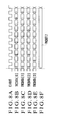
- the trace information output unit 515 which has received the trace data, outputs trace data of format 3 (Fig. 6C) as the TRCDATAO-3 signal 518 (Figs. 8B to 8E) in synchronism with the leading edge of the CLKOUT signal 505 (Fig. 8A).
- the TRCDATAO-3 signal 518 is output in units of 4 bits from the least significant bit at the timing of packet 2' (Fig. 8F).
- the microcomputer 500 executes processes I) to III). In this case, completing output of trace information for the branch instruction requires 10 clocks, as shown in Figs. 7A to 7F. However, most of the recent microcomputers operate in accordance with a branch instruction at nine clocks or less because of a high-speed operation request. Even if, therefore, the next write instruction is to be executed upon completion of the branch instruction, trace information for the branch instruction has not been completed yet.
- the trace information generator 514 cannot perform process IV) until the trace information output unit 515 outputs all the trace information (buffer overflow). Thus, in consecutive processing, the trace information generator 514 generates pseudo trace information represented by format 1 in Fig. 6A, and sends the information to the trace information output unit 515.
- the trace information output unit 515 outputs the pseudo trace information in units of 4 bits from the least significant bit at the timing of packet 2 shown in Fig. 7F.
- the microcomputer incorporating the debugging function suffers the above problems because the real chip function is the main, and the number of trace buffers or trace information output terminals cannot be increased.
- a microcomputer comprising an internal memory storing a control program, a CPU (Central Processing Unit) core for executing the control program stored in the internal memory, the CPU core outputting a control signal made up of connection information containing a storage address of the control program in the internal memory and an address of the internal memory generated as a result of executing the control program, instruction contents of the control program, and data generated by executing the control program, bus control means for controlling signal exchange based on an operation of the CPU core via an address bus and a data bus that are connected to an external memory, the bus control means having data I/O control means for, when the control signal is received from the CPU core, outputting an address obtained from the connection information in the control signal to the external address bus, and outputting the data in the control signal to the external data bus, and debugging control means for generating trace information necessary for debugging operation for confirming an operation by the control program, the debugging control means having trace information generation means for extracting the instruction contents in the control signal
- a microcomputer 100 is constituted by a debugging controller 101, CPU core 102, bus controller 103, and internal memory 120.
- the bus controller 103 comprises a data I/O controller 112 for exchanging an address value with an external address bus 107 and exchanging data with an external data bus 108 on the basis of the control signal 106 from the CPU core 102, and a priority processing controller 113 for instructing priority processing based on a predetermined priority when trace information output processing and access processing to an external memory (not shown) collide with each other.
- the bus controller 103 performs processing of outputting an active-high write signal MWR 109 to the external memory (not shown).
- the debugging controller 101 comprises a trace information generator 110 for generating trace information in accordance with the control signal 106, and a trace information output unit 111 for outputting the trace information output from the trace information generator 110 as a TRCDATA0-3 signal 104 in time division.
- the microcomputer 100 gives priority to output of debugging information.
- This priority processing control is done by the priority processing controller 113 of the bus controller 103.
- the priority processing controller 113 instructs the debugging controller 101 and data I/O controller 112 to perform priority processing.
- the priority processing controller 113 may instruct only a controller which performs lower-priority processing, i.e., the data I/O controller 112 to suspend the processing.
- the trace information generator 110 generates trace information of a trace buffer overflow when the generator 110 receives the control signal 106 from the CPU core 102 as a result of executing a next instruction before the trace information output unit 111 outputs all trace information as the TRCDATA0-3 signal 104.
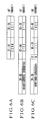
- a trace packet format used in the microcomputer 100 having this arrangement will be described with reference to Figs. 2A to 2C.
- every trace packet is made up of 8 bits. Lower four bits represent trace information. As shown by formats 1 to 3 in Figs. 2A to 2C, "0011” represents the overflow of the trace buffer, "0110” represents execution of a branch instruction, and "1001" represents execution of data access.
- the branch instruction is located at an address "000000H” in the internal memory 120 of the microcomputer 100, and is a branch instruction to an address "000010H".
- the write instruction is located at an address "000010H” in the internal memory 120, and a write instruction of writing 32-bit data "5A5A5A5AH" at an address "001000H”.
- the address bus width is 24 bits
- the data bus width is 32 bits
- the trace buffer is made up of 4 bits equal in number to the terminals of the trace information output.
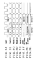
- the microcomputer 100 To execute a branch instruction to the address "000010H” that is located at the address "000000H” in the internal memory 120, the microcomputer 100 performs processing in the following order.
- the data I/O controller 112 of the bus controller 103 Upon reception of the control signal 106, the data I/O controller 112 of the bus controller 103 outputs the branch source address "00000000H" to the external address bus 107 at the timing of bus cycle 1 (Fig. 3H).
- the CPU core 102 fetches a data write instruction from the address "000010H” in the internal memory 120, and executes the instruction.
- the CPU core 102 outputs, to the bus controller 103 and debugging controller 101, the control signal 106 instructing output of address data "000010H” to the external address bus 107 and output of write data "5A5A5A5AH" to the external data bus 108.
- the trace information generator 110 in the debugging controller 101 Upon reception of the control signal 106, the trace information generator 110 in the debugging controller 101 generates 8-bit trace data of format 3 (Fig. 2C), and outputs it to the trace information output unit 111.
- the trace information output unit 111 which has received the trace data, outputs trace data as the TRCDATA0-3 signal 104 (Figs. 3B to 3E).
- a packet of format 3 As the TRCDATA0-3 signal 104, a packet of format 3 (Fig. 2C) is output in units of 4 bits from the least significant bit at the timing of packet 2 in synchronism with the leading edge of the CLKOUT signal 105 (Fig. 3A).
- the debugging controller 101 does not perform the conventional operation of loading data on a PC trace bus or emulation/data trace bus into the trace buffer or outputting the TRCDATA0-3 signal in time division in outputting trace information.
- the bus controller 103 outputs, to the external address bus and external data bus, the address of an instruction executed by the CPU core 102, the address at which the branch destination and data are stored, a data destination address, or data.
- a microcomputer 400 in this embodiment is constituted by a debugging controller 101, CPU core 102, bus controller 401, and internal memory 120.
- the debugging controller 101, CPU core 102, and internal memory 120 are identical to those in Fig. 1, and a description thereof will be omitted.
- the bus controller 401 comprises a data I/O controller 402 and priority processing controller 403.
- the data I/O controller 402 exchanges an address value with an external address bus 107, and exchanges data with an external data bus 108 on the basis of a control signal 106 from the CPU core 102. In exchanging an address value and data, a write signal MWR 109 is output to an external memory (not shown).
- the priority processing controller 403 performs control of preferentially executing write operation in the external memory (not shown).
- the MWR signal 109 is an active-high signal.
- the priority processing controller 113 controls to perform trace information priority processing. This impairs real-time execution.
- the priority processing controller 403 informs the debugging controller 101 and data I/O controller 402 that priority is given to write processing to the external memory (not shown). After write processing to the external memory (not shown) ends, the microcomputer performs the same processing as in executing a branch instruction and accessing the internal memory 120. Hence, real-time execution of the microcomputer 400 is not impaired.
- the debugging controller does not process any trace information, which greatly reduces the number of overflows of the trace buffer used in the debugging controller, compared to the conventional microprocessor. Consequently, the debugging efficiency in the microcomputer incorporating the debugging function can increase.
Landscapes
- Engineering & Computer Science (AREA)
- Theoretical Computer Science (AREA)
- Computer Hardware Design (AREA)
- Quality & Reliability (AREA)
- Physics & Mathematics (AREA)
- General Engineering & Computer Science (AREA)
- General Physics & Mathematics (AREA)
- Debugging And Monitoring (AREA)
- Microcomputers (AREA)
- Test And Diagnosis Of Digital Computers (AREA)
Abstract
Description
Claims (8)
- A microcomputer characterized by comprising:an internal memory (120) storing a control program;a CPU (Central Processing Unit) core (102) for executing the control program stored in said internal memory, said CPU core outputting a control signal made up of connection information containing a storage address of the control program in said internal memory and an address of said internal memory generated as a result of executing the control program, instruction contents of the control program, and data generated by executing the control program;bus control means (103, 401) for controlling signal exchange based on an operation of said CPU core via an address bus and a data bus that are connected to an external memory, said bus control means having data I/O control means (112) for, when the control signal is received from said CPU core, outputting an address obtained from the connection information in the control signal to the external address bus, and outputting the data in the control signal to the external data bus; anddebugging control means (101) for generating trace information necessary for debugging operation for confirming an operation by the control program, said debugging control means having trace information generation means (110) for extracting the instruction contents in the control signal as trace information when the control signal is received from said CPU core, and trace information output means (111) for externally outputting the trace information output from said trace information generation means.
- A microcomputer according to claim 1,
wherein said bus control means (103) comprises priority processing control means (113) for preferentially performing trace information output processing when trace information output processing by said debugging control means collides with signal exchange processing with the external memory by said data I/O control means. - A microcomputer according to claim 1,
wherein said priority processing control means instructs at least said data I/O control means to suspend signal exchange processing with the external memory when two processes collide with each other. - A microcomputer according to claim 1,
wherein said bus control means (401) comprises priority processing control means (403) for preferentially performing signal exchange with the external memory when trace information output by said debugging control means collides with signal exchange with the external memory by said data I/O control means. - A microcomputer according to claim 4,
wherein said priority processing control means instructs at least said debugging control means to suspend trace information output processing when two processes collide with each other. - A microcomputer according to claim 1,
wherein the trace information is made up of an 8-bit signal. - A microcomputer according to claim 1,
wherein said bus control means outputs an active-high signal representing effective write to the external memory in outputting an address and data to the external address bus and the external data bus, respectively. - A microcomputer according to claim 1, further comprising any combination of the features set forth in claims 2 to 7.
Applications Claiming Priority (2)
| Application Number | Priority Date | Filing Date | Title |
|---|---|---|---|
| JP15626599A JP3289704B2 (en) | 1999-06-03 | 1999-06-03 | Microcomputer |
| JP15626599 | 1999-06-03 |
Publications (3)
| Publication Number | Publication Date |
|---|---|
| EP1058189A2 true EP1058189A2 (en) | 2000-12-06 |
| EP1058189A3 EP1058189A3 (en) | 2003-07-16 |
| EP1058189B1 EP1058189B1 (en) | 2010-07-14 |
Family
ID=15624039
Family Applications (1)
| Application Number | Title | Priority Date | Filing Date |
|---|---|---|---|
| EP00111716A Expired - Lifetime EP1058189B1 (en) | 1999-06-03 | 2000-05-31 | Microcomputer with debugging system |
Country Status (3)
| Country | Link |
|---|---|
| EP (1) | EP1058189B1 (en) |
| JP (1) | JP3289704B2 (en) |
| DE (1) | DE60044660D1 (en) |
Cited By (4)
| Publication number | Priority date | Publication date | Assignee | Title |
|---|---|---|---|---|
| WO2002086728A1 (en) * | 2001-04-20 | 2002-10-31 | Infineon Technologies Ag | Program-controlled unit |
| US6973592B2 (en) * | 2000-10-18 | 2005-12-06 | Stmicroelectronics Limited | On-chip emulator communication |
| US6973591B2 (en) * | 2000-10-18 | 2005-12-06 | Stmicroelectronics Limited | On-chip emulator communication for debugging |
| CN107038116A (en) * | 2017-03-16 | 2017-08-11 | 杭州朔天科技有限公司 | The implementation method of small nut program is debugged in multi-core chip system by big core |
Families Citing this family (4)
| Publication number | Priority date | Publication date | Assignee | Title |
|---|---|---|---|---|
| JP2008071227A (en) * | 2006-09-15 | 2008-03-27 | Nec Electronics Corp | Semiconductor integrated circuit |
| JP5850732B2 (en) * | 2011-12-14 | 2016-02-03 | ルネサスエレクトロニクス株式会社 | Semiconductor device and control method thereof |
| JP6142182B2 (en) * | 2013-04-16 | 2017-06-07 | ナルテック株式会社 | Integrated circuit device |
| CN109284223B (en) * | 2017-07-21 | 2023-10-20 | 超威半导体(上海)有限公司 | Configurable debugging method and system |
Family Cites Families (6)
| Publication number | Priority date | Publication date | Assignee | Title |
|---|---|---|---|---|
| US5491793A (en) * | 1992-07-31 | 1996-02-13 | Fujitsu Limited | Debug support in a processor chip |
| JPH086918A (en) * | 1994-06-15 | 1996-01-12 | Nec Corp | Microcomputer |
| US5964893A (en) * | 1995-08-30 | 1999-10-12 | Motorola, Inc. | Data processing system for performing a trace function and method therefor |
| JP3260083B2 (en) * | 1996-09-03 | 2002-02-25 | 株式会社東芝 | Debug system and debugging method |
| EP0869434A3 (en) * | 1997-03-31 | 1999-09-15 | Hewlett-Packard Company | Method for outputting trace information of a microprocessor |
| JP2000242523A (en) | 1999-02-22 | 2000-09-08 | Toshiba Corp | Microprocessor and debug device |
-
1999
- 1999-06-03 JP JP15626599A patent/JP3289704B2/en not_active Expired - Fee Related
-
2000
- 2000-05-31 EP EP00111716A patent/EP1058189B1/en not_active Expired - Lifetime
- 2000-05-31 DE DE60044660T patent/DE60044660D1/en not_active Expired - Lifetime
Cited By (5)
| Publication number | Priority date | Publication date | Assignee | Title |
|---|---|---|---|---|
| US6973592B2 (en) * | 2000-10-18 | 2005-12-06 | Stmicroelectronics Limited | On-chip emulator communication |
| US6973591B2 (en) * | 2000-10-18 | 2005-12-06 | Stmicroelectronics Limited | On-chip emulator communication for debugging |
| WO2002086728A1 (en) * | 2001-04-20 | 2002-10-31 | Infineon Technologies Ag | Program-controlled unit |
| US7281162B2 (en) | 2001-04-20 | 2007-10-09 | Infineon Technologies Ag | Program-controlled unit |
| CN107038116A (en) * | 2017-03-16 | 2017-08-11 | 杭州朔天科技有限公司 | The implementation method of small nut program is debugged in multi-core chip system by big core |
Also Published As
| Publication number | Publication date |
|---|---|
| EP1058189B1 (en) | 2010-07-14 |
| EP1058189A3 (en) | 2003-07-16 |
| JP3289704B2 (en) | 2002-06-10 |
| JP2000347899A (en) | 2000-12-15 |
| DE60044660D1 (en) | 2010-08-26 |
Similar Documents
| Publication | Publication Date | Title |
|---|---|---|
| US6075941A (en) | Microcomputer | |
| US5608867A (en) | Debugging system using virtual storage means, a normal bus cycle and a debugging bus cycle | |
| JPH06314213A (en) | Debugging device | |
| EP0902367B1 (en) | Data processing unit with debug capabilities | |
| EP1058189B1 (en) | Microcomputer with debugging system | |
| US6839869B2 (en) | Trace control circuit for tracing CPU operation in real time | |
| KR900004291B1 (en) | A method and apparatus for coordinating exceution of an instruction by a processor | |
| US4667285A (en) | Microcomputer unit | |
| EP0638864B1 (en) | Development support system for microcomputer with internal cache | |
| JP2877095B2 (en) | Multiprocessor system | |
| JPH1078887A (en) | Debug system and debugging method | |
| CN119783603B (en) | Multi-platform fusion verification system | |
| JPH08272770A (en) | Microcontroller Development System | |
| US6854047B2 (en) | Data storage device and data transmission system using the same | |
| JP2940309B2 (en) | Microcomputer for program development | |
| JP2000029508A (en) | Programmable controller | |
| JPH06324906A (en) | Single chip microcomputer | |
| JP3120841B2 (en) | In-circuit emulator | |
| JPH1165884A (en) | Microcomputer and debugging method therefor | |
| JPH10312307A (en) | Emulator applied to computer system | |
| JP2954006B2 (en) | Emulation device and emulation method | |
| JPH10187480A (en) | emulator | |
| JPH10326266A (en) | Microcomputer | |
| JPH0259829A (en) | Microcomputer | |
| JP2002082819A (en) | Semiconductor integrated circuit device |
Legal Events
| Date | Code | Title | Description |
|---|---|---|---|
| PUAI | Public reference made under article 153(3) epc to a published international application that has entered the european phase |
Free format text: ORIGINAL CODE: 0009012 |
|
| AK | Designated contracting states |
Kind code of ref document: A2 Designated state(s): AT BE CH CY DE DK ES FI FR GB GR IE IT LI LU MC NL PT SE |
|
| AX | Request for extension of the european patent |
Free format text: AL;LT;LV;MK;RO;SI |
|
| RAP1 | Party data changed (applicant data changed or rights of an application transferred) |
Owner name: NEC ELECTRONICS CORPORATION |
|
| PUAL | Search report despatched |
Free format text: ORIGINAL CODE: 0009013 |
|
| AK | Designated contracting states |
Designated state(s): AT BE CH CY DE DK ES FI FR GB GR IE IT LI LU MC NL PT SE |
|
| AX | Request for extension of the european patent |
Extension state: AL LT LV MK RO SI |
|
| RIC1 | Information provided on ipc code assigned before grant |
Ipc: 7G 06F 11/00 A Ipc: 7G 06F 11/36 B |
|
| 17P | Request for examination filed |
Effective date: 20031027 |
|
| AKX | Designation fees paid |
Designated state(s): DE GB |
|
| 17Q | First examination report despatched |
Effective date: 20040503 |
|
| 17Q | First examination report despatched |
Effective date: 20040503 |
|
| GRAP | Despatch of communication of intention to grant a patent |
Free format text: ORIGINAL CODE: EPIDOSNIGR1 |
|
| GRAS | Grant fee paid |
Free format text: ORIGINAL CODE: EPIDOSNIGR3 |
|
| GRAA | (expected) grant |
Free format text: ORIGINAL CODE: 0009210 |
|
| AK | Designated contracting states |
Kind code of ref document: B1 Designated state(s): DE GB |
|
| REG | Reference to a national code |
Ref country code: GB Ref legal event code: FG4D |
|
| REF | Corresponds to: |
Ref document number: 60044660 Country of ref document: DE Date of ref document: 20100826 Kind code of ref document: P |
|
| RAP2 | Party data changed (patent owner data changed or rights of a patent transferred) |
Owner name: RENESAS ELECTRONICS CORPORATION |
|
| PLBE | No opposition filed within time limit |
Free format text: ORIGINAL CODE: 0009261 |
|
| STAA | Information on the status of an ep patent application or granted ep patent |
Free format text: STATUS: NO OPPOSITION FILED WITHIN TIME LIMIT |
|
| 26N | No opposition filed |
Effective date: 20110415 |
|
| REG | Reference to a national code |
Ref country code: DE Ref legal event code: R097 Ref document number: 60044660 Country of ref document: DE Effective date: 20110415 |
|
| GBPC | Gb: european patent ceased through non-payment of renewal fee |
Effective date: 20110531 |
|
| PG25 | Lapsed in a contracting state [announced via postgrant information from national office to epo] |
Ref country code: GB Free format text: LAPSE BECAUSE OF NON-PAYMENT OF DUE FEES Effective date: 20110531 |
|
| PGFP | Annual fee paid to national office [announced via postgrant information from national office to epo] |
Ref country code: DE Payment date: 20150527 Year of fee payment: 16 |
|
| REG | Reference to a national code |
Ref country code: DE Ref legal event code: R119 Ref document number: 60044660 Country of ref document: DE |
|
| PG25 | Lapsed in a contracting state [announced via postgrant information from national office to epo] |
Ref country code: DE Free format text: LAPSE BECAUSE OF NON-PAYMENT OF DUE FEES Effective date: 20161201 |