The present invention relates to a transparent layered product
including a glass sheet and a coating film with a rough surface and a glass
article using the same (for example, a photoelectric conversion device, a
multiple-glazing unit, or the like).
A transparent layered product in which a thin film such as a tin
oxide film or the like is formed on a glass sheet has been used widely for a
thin film photoelectric conversion device (a thin film solar cell), heat-reflecting
glass, or the like. For example, JP 7-29402 B describes heat-reflecting
glass formed by stacking a silicon film, a silicon oxide film, and a
tin oxide film on a glass sheet in this order.
Tin oxide in a film formed by pyrolysis on a high-temperature
substrate becomes a polycrystalline film. The polycrystalline product of tin
oxide has a surface with roughness caused by the growth of crystal grains
according to the increase in film thickness. In a thin film photoelectric
conversion device, the surface roughness of a tin oxide film as a transparent
electrode enables photovoltaic characteristics to be improved due to a light
trapping effect.
For example, JP 61-288473 A discloses a thin film photoelectric
conversion device including a tin oxide film having a rough surface including
convex portions with heights in the range between 100 and 500 nm and
intervals between respective convex portions in the range between 200 and
1000 nm. The rough surface is formed by etching after film formation.
Further, JP 2-503615 A discloses a substrate for a thin film
photoelectric conversion device including a tin oxide film having a surface
provided with convex portions with diameters in the range between 0.1 and
0.3 µm and the ratio of height/diameter in the range between 0.7 and 1.2.
In addition, JP 2-503615 A also discloses a chemical vapor deposition method
(a CVD method) using a mixed gas containing tin tetrachloride, water vapor,
methyl alcohol, nitrogen and the like, which is carried out on a precut glass
sheet, as a method of manufacturing a tin oxide film.
JP 4-133360 A discloses a substrate for a thin film photoelectric
conversion device including a tin oxide film having a surface with pyramidal
convex portions with heights in the range between 100 and 300 nm and
angles with respect to the normal line of the principal plane of the substrate
in the range between 30° and 60°. Similarly, JP 4-133360 A also discloses a
CVD method using a mixed gas containing tin tetrachloride, oxygen,
nitrogen and the like, which is carried out on a glass sheet with a
temperature in the range between 350 and 500°C, as a method of
manufacturing a tin oxide film.
Besides the tin oxide film, coating films formed of zinc oxide, ITO
(indium tin oxide), titanium oxide, silicon oxide or the like also are formed on
a glass sheet to add various functions. These coating films are formed on a
glass sheet as, for example, a reflection-suppression film, an electromagnetic
shielding film, an antifouling film, a low-emissivity film (Low-E film), or as a
component thereof, in addition to a transparent conductive film and a heat
reflecting film.
As described above, when a transparent layered product is obtained
by forming a crystalline or amorphous coating film for adding various
functions to a glass sheet, the light reflectance may be higher than that
required in some cases. In addition, for example, when the transparent
layered product is used as a substrate for a photoelectric conversion device or
reflection-suppression glass, a lower reflectance is preferable. Depending
on the intended use, the coloring of reflected light due to the formation of the
coating film may be intended to be suppressed to a degree causing no harm
to the desired appearance in some cases.
Judging from the fact that a porous surface has a refractive index
distribution in the depth direction, it is conceivable that a transition layer in
which the refractive index varies continuously is present at the surface of a
coating film such as a tin oxide film or the like. This transition layer can
affect reflected light from the transparent layered product. Conventionally,
particularly in the field of photoelectric conversion devices, the heights and
intervals of convex portions of the rough surface of a tin oxide film have been
adjusted. Conventionally, however, attention merely has been paid to the
physical shape and size of convex or concave portions of the rough surface.
The refractive index distribution in the transition layer produced at the
surface of a coating film does not depend only on the shape and size of the
individual convex or concave portions of the rough surface but also is affected
by the distribution of them. Therefore, the refractive index distribution in
the transition layer should not be evaluated based on observation of the
rough surface in a very limited region by an electron microscope and is
required to be evaluated based on optical measurement.
It is an object of the present invention that in a transparent layered
product including a glass sheet and a coating film exhibiting various
functions, the reflectance of light entering the transparent layered product is
decreased by suitably controlling the refractive index distribution in a
transition layer at the surface of the coating film. Further, another object of
the present invention is to provide a glass article using this transparent
layered product, particularly a multiple-glazing unit and a photoelectric
conversion device such as a photovoltaic device.
The present inventors found that surprisingly, the aforementioned
objects were able to be achieved by controlling the pattern of the variation in
refractive index in a thickness direction in a transition layer present at the
surface of the coating film.
The transparent layered product of the present invention includes a
glass sheet and a coating film having a surface with roughness, which is
formed on the glass sheet, and a transition layer in which the refractive
index varies continuously in its thickness direction is present at the surface
of the coating film. The variation in refractive index in the transition layer
is indicated by a convex curve over the whole region of the transition layer,
when the variation is shown on a plane defined by a horizontal axis
indicating the refractive index and a vertical axis indicating the thickness
direction of the transition layer, with the glass sheet positioned on a lower
side.
When the coating film is formed as an outermost layer, the
refractive index in the transition layer varies continuously in its thickness
direction to approach the refractive index of air (1) from the refractive index
of the coating film, in the direction of the outside air. On the other hand,
when another thin film is further formed on the coating film having a surface
with roughness, the refractive index in the transition layer approaches the
refractive index of the another thin film while varying continuously in its
thickness direction. In this case, it is preferable that the refractive index
varies continuously from a refractive index n1 of the coating film to a
refractive index n2 of the thin film formed thereon so that the variation in
refractive index is indicated by a convex locus (curve) over the whole region
when being shown on a plane. The magnitude correlation between the
refractive index n1 and the refractive index n2 is not particularly limited.
In the transparent layered product, it is preferable that the coating
film is a crystalline coating film. It also is preferable that the roughness is
caused by crystal grains in the crystalline coating film. In this connection,
the crystalline coating film may contain amorphous portions regionally, and
a film with a crystalline fraction in volume of at least 50% as a whole is
taken as corresponding to a "crystalline" film.
In the transparent layered product, it is preferable that the
crystalline coating film contains, as a main component, at least one selected
from tin oxide, zinc oxide, indium oxide, and titanium oxide. Particularly, a
coating film containing tin oxide as the main component is useful for many
purposes. In this specification, the "main component" denotes a component
accounting for at least 50 wt.% of the whole amount.
In the transparent layered product, it is preferable that the coating
film is formed on an undercoating film on the glass sheet. In this case, it is
further preferable that the undercoating film is a coating film formed by
pyrolysis of a material containing halogen, and the coating film has a surface
with roughness caused by production of or loss after the production of
compound grains of an alkaline component in the glass sheet and the
halogen. Utilization of the roughness enables a transition layer having the
above-mentioned refractive index distribution to be obtained easily.
In the transparent layered product, the roughness caused by a
reaction product of the alkaline component in the glass may be utilized
directly. In other words, in the transparent layered product of the present
invention, the coating film having a surface with roughness may be a coating
film formed by pyrolysis of a material containing halogen, and the coating
film formed by pyrolysis may have a surface with roughness caused by
production of or loss after the production of compound grains of an alkaline
component in the glass sheet and the halogen. Particularly, when such
production of compound grains is utilized, the coating film having a surface
with roughness is not required to be a crystalline coating film.
In the transparent layered product, it is preferable that the
thickness of the transition layer in the coating film corresponds to 30% or
lower of the thickness of a layer having a substantially constant refractive
index in the coating film. The thickness of the transition layer is not
particularly limited,but preferably corresponds to at least 10% of the
thickness of the layer having a substantially constant refractive index in the
coating film.
In the transparent layered product, the coating film having a
surface with roughness may be an insulating coating film, but a conductive
coating film (a transparent conductive film) is used in a photoelectric
conversion device or the like.
The transparent layered product can be used for various purposes.
For example, it can be used as reflection-suppression (anti-reflection) glass,
electromagnetic shielding glass, glass to be electrified for preventing fogging
or the like, antifouling glass, antistatic glass, low-emissivity glass (Low-E
glass), glass for information display equipment (for instance, a touch control
panel), or glass for a top plate of a duplicator.
The transparent layered product may be used as a glass article by
being combined with other members. For example, the present invention
includes a multiple-glazing unit in which at least two transparent substrates
are positioned to face each other via at least one inner layer selected from a
group consisting of an air layer, an inert gas layer, and a low pressure layer
and at least one of the transparent substrates is the transparent layered
product. Furthermore, the multiple-glazing unit may be used for a door of a
refrigerator (a refrigerated display case), and the conductive coating film (a
coating film having a surface with roughness) included in the multiple-glazing
unit is used as a heating element. In this case, the refrigerator is
provided with an electrification device for passing a current in the conductive
coating film.
In addition, for example, when the transparent layered product of
the present invention is used in information display equipment, this
information display equipment displays information through the
transparent layered product. This information display equipment is
provided with a display device for displaying information and the conductive
film included in the transparent layered product serves as a transparent
electrode. Furthermore, for instance, when the transparent layered product
of the present invention is used in a duplicator, this duplicator optically
reads information to be duplicated through the transparent layered product.
In this case, the transparent layered product is used as a top plate (a
document glass on which an original is placed) of the duplicator, and the
conductive coating film included in the transparent layered product serves as
an antistatic film.
The transparent layered product also can be used as a substrate for
a photoelectric conversion device. The photoelectric conversion device
includes: a transparent layered product having a glass sheet and a
conductive crystalline coating film having a surface with roughness, which is
formed on the glass sheet; at least one photoelectric conversion unit; and a
back electrode. The surface roughness is caused by crystal grains in the
crystalline coating film, and the crystalline coating film includes, at its
surface, a transition layer in which the refractive index varies continuously
in its thickness direction. The photoelectric conversion unit and the back
electrode are stacked in this order on the crystalline coating film. When a
variation in the refractive index in the transition layer is shown on a plane
defined by a horizontal axis indicating the refractive index and a vertical
axis indicating the thickness direction of the transition layer, with the glass
sheet positioned on a lower side, the variation in the refractive index is
indicated by a convex curve over a whole region of the transition layer.
Preferable embodiments according to the present invention are
described as follows.
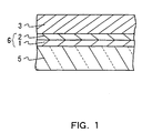
FIG. 1 is a sectional view of an embodiment of the transparent
layered product according to the present invention. In this transparent
layered product, an undercoating film 6 including a first undercoating layer
1 and a second undercoating layer 2, and a crystalline coating film 3 are
formed on a glass sheet 5 in this order.
The following description is directed to a preferable embodiment
when the crystalline coating film 3 is used as a transparent electrode in a
photoelectric conversion device. As the crystalline coating film, a tin oxide
film doped with a trace element such as fluorine, antimony, or the like,
specifically a fluorine-containing tin oxide film (a SnO2:F film) doped with
fluorine at a predetermined concentration is preferable. Preferably, the
fluorine concentration in the film is 0.15 wt.% or lower. This film has a
refractive index of about 1.9. This crystalline coating film may contain
other trace components such as silicon, aluminum, zinc, copper, indium,
bismuth, gallium, boron, vanadium, manganese, zirconium, or the like.
Preferably, however, the total concentration of such trace components is 0.02
wt.% or lower. It is preferable that the sheet resistance of the crystalline
coating film is, specifically, in the range between 5Ω /sq.(Ω/□) and 25Ω/sq.
In view of this sheet resistance, the preferable thickness of the crystalline
coating film 3 is in the range between 400 nm and 1200 nm.
It is preferable that the first undercoating layer 1 has a thickness in
the range between 5 nm and 100 nm and a refractive index in the range
between 1.6 and 2.5. Preferably, the first undercoating layer 1 is formed of
at least one selected from tin oxide, titanium oxide, and aluminum oxide. It
is preferable that the second undercoating layer 2 has a thickness in the
range between 5 nm and 100 nm and a refractive index in the range between
1.4 and 2.0. Preferably, the second undercoating layer 2 is formed of at least
one selected from silicon oxide, aluminum oxide, and tin oxide.
Furthermore, it is preferable that the refractive index of the first
undercoating layer is higher than that of the second undercoating layer.
The structure of the undercoating film 6 is not limited to the two-layer
structure, and the undercoating film 6 may be formed of a single layer
or three layers or more. A layer in which the refractive index varies
continuously may be included between the first undercoating layer and the
second undercoating layer. Further, in order to improve plasma resistance,
a protective film (for instance, a zinc oxide film) may be formed on the
crystalline coating film.
Layers included in the undercoating film may contain, as a main
component, an oxide containing at least two metals such as, for example,
silicon-tin oxide (SiSnO). Other preferable examples of the layers include a
film containing, as a main component, oxycarbide such as for instance silicon
oxycarbide (SiOC), or oxynitride. Generally, an oxycarbide film or an
oxynitride film in which carbon or nitrogen is introduced has a slightly
higher refractive index than that of an oxide film.
As described above, the transparent layered product of the present
invention can be used not only for a photoelectric conversion device but also
in a wide variety of technical fields. The structure, type, and thickness of a
coating film are determined suitably depending on the intended use of the
transparent layered product. The following description is directed to an
example of a preferable embodiment when the transparent layered product
is used as heat-reflecting glass. Heat-reflecting glass may cause harmful
light reflection to the surroundings when having an excessively high visible-light
reflectance. Therefore, the above-mentioned transparent layered
product also is useful as heat-reflecting glass.
When the transparent layered product is used as heat-reflecting
glass, it is preferable that the crystalline coating film 3 is a tin oxide film.
To this tin oxide film, other trace components may be added as described
above. It is preferable that the crystalline coating film 3 has a thickness in
the range between 5 nm and 20 nm. It is preferable that the first
undercoating layer 1 has a thickness in the range between 5 nm and 100 nm
and a refractive index in the range between 2.5 and 5.0. Preferably, the
first undercoating layer 1 is formed of silicon. It is preferable that the
second undercoating layer 2 has a thickness in the range between 5 nm and
100 nm and a refractive index in the range between 1.45 and 1.8.
Preferably, the second undercoating layer 2 is formed of at least one selected
from silicon oxide and aluminum oxide. Further, it is preferable that the
refractive index of the first undercoating layer is higher than that of the
second undercoating layer. Similarly in this case, the structure of the
undercoating film 6 is not limited to the two-layer structure, and the
undercoating film 6 may be formed of a single layer or three layers or more.
In the above, a transition layer derived from the surface roughness
caused by the growth of crystal grains in the crystalline coating film was
described. However, the transition layer may be derived from the
roughness caused by, in the film, the presence of or the loss after production
of a compound of sodium halide or the like produced on the glass sheet
surface. In the case where a coating film is formed by thermally
decomposing (pyrolyzing) a material containing chlorine on a glass surface,
particularly when the surface temperature of the glass is high, the chlorine
and sodium contained in the glass react to produce sodium chloride easily.
From the examples described later, it was confirmed that the transition layer
in which the variation in refractive index was indicated by a convex curve
appeared at the surface of a coating film in which holes formed of the sodium
chloride and by the loss of the sodium chloride produced were recognized.
Similarly, in the case where a crystalline coating film is formed on an
undercoating film, when the undercoating film is formed under conditions
allowing sodium chloride to be produced easily, the transition layer of the
crystalline coating film formed on the undercoating film tends to have
refractive indexes whose variation is indicated by a convex curve.
In the above-mentioned transition layer, the variation in refractive
index per unit thickness is not constant, and typically increases with
distance from the glass sheet. This variation in refractive index is indicated
by a convex curve in a graph over the whole region, when a horizontal axis
indicates the refractive index and a vertical axis indicates the thickness
direction of the transition layer, with the glass sheet positioned on the lower
side. Generally, it is conceivable that such a locus of the variation in
refractive index can be obtained easily when the crystal grains in the coating
film have a dome shape. However, it also has been confirmed that such a
locus of the variation in refractive index as described above can be obtained
even when the surface has a crater shape obtained by inverting the dome
shape.
It is preferable that when the coating film is used as an outermost
layer, the refractive index of the transition layer varies continuously in its
thickness direction from the refractive index of the coating film (for example,
a refractive index of about 1.9 of tin oxide) to the refractive index of air (1).
On the other hand, it is preferable that when a thin film is further formed on
the coating film as in the case where the transparent layered product is used
in a thin film solar cell, the refractive index in the transition layer varies
continuously from the refractive index of the crystalline coating film (for
example, about 1.9) to the refractive index of the thin film on the coating film
(for instance, a refractive index of about 4.7 of amorphous silicon or a
refractive index of about 2.8 of amorphous silicon carbide).
Further, it is preferable that the thickness of the transition layer
corresponds to 30% or less of the thickness of the layer (a nontransition
layer) having a substantially constant refractive index in the coating film.
The reason is that when the ratio in thickness of the transition layer is 30%
or less, the nontransition layer has a sufficient thickness, thus obtaining a
transparent layered product taking advantage of the characteristics in
refractive index of the coating film. In addition, it is preferable that the
thickness of the transition layer corresponds to at least 10 % of that of the
nontransition layer. When the ratio in thickness of the transition layer is at
least 10 %, the function of the transition layer in which the refractive index
varies continuously tends to be exhibited easily.
The transition layer in which the variation in refractive index is
indicated by a convex curve in the graph as described above can have a lower
light reflectance than that of a transition layer in which the variation in
refractive index is substantially constant.
One of the methods of manufacturing the transition layer is a
pyrolytic method, particularly a CVD method on a glass ribbon in a glass
sheet production line by a float glass process. The manufacturing method of
the transparent layered product according to the present invention is not
limited to the CVD method on a glass ribbon. It has not been confirmed
that the transition layer is formed without fail when a film is deposited on a
glass ribbon, but the CVD method satisfies at least conditions suitable for
the formation of the transition layer.
The reason that the transition layer is obtained by the film
deposition on a high-temperature glass ribbon by the CVD method has not
been confirmed. However, it is assumed that the crystalline nucleus
present at the surface of the glass ribbon has an influence on the transition
layer. When the crystalline nucleus is present at the glass surface, the
growth of the crystal grains in a crystalline coating film is affected even
when the coating film is formed on an undercoating film. It is conceivable
that besides sodium chloride described above, for example, tin particles
adhering to the surface of the glass ribbon in a float bath also contribute to
the growth of the crystalline nucleus. Further, as described above, due to
the produced sodium chloride itself, the transition layer tends to be formed
easily.
According to the CVD method on a glass ribbon, thermal energy in
forming glass also can be utilized. This preferable manufacturing method is
particularly suitable for manufacturing a substrate for a photoelectric
conversion device or low-emissivity glass, which may be required to be
manufactured as a large product for a large window glass, roofing material,
or the like. Particularly, when the CVD method is carried out in a float bath,
the film deposition can be carried out on the surface of glass having a
temperature equal to or higher than the softening point. The film
deposition at a high temperature enables the improvements in film
performance, film growth rate, and film deposition reaction efficiency. In
addition, defects such as pinholes can be suppressed.
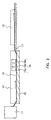
FIG. 2 shows an embodiment of a device for depositing a film on a
glass ribbon in the float glass process by the CVD method. As shown in FIG.
2, in this device, a predetermined number of coaters 16 (three coaters 16a,
16b, and 16c in the embodiment shown in the figure) are placed at a
predetermined distance from the surface of a glass ribbon 10. The glass
ribbon 10 is formed from molten glass, which is poured from a furnace 11 into
a float bath 12, in a belt-like form on a tin bath 15 while traversing the
length of the float bath 12. The number and arrangement of the coaters are
selected suitably depending on the kind and thickness of a coating film to be
formed. These coaters supply gaseous materials to form coating films on
the glass ribbon 10 continuously. When a plurality of coaters are used, an
undercoating film and a crystalline coating film can be formed on the glass
ribbon 10 successively by the CVD method. The glass ribbon 10 on which
the coating films including the crystalline coating film have been formed is
lifted by a roller 17 and is carried into an annealing furnace 13. The glass
ribbon 10 annealed in the annealing furnace 13 is cut by a cutting device,
which is not shown in the figure, thus obtaining a glass sheet with a
predetermined size.
Examples of the tin material in the case of using the CVD method
include tin tetrachloride, dimethyltin dichloride, dibutyltin dichloride,
tetramethyltin, tetrabutyltin, dioctyltin dichloride, monobutyltin trichloride,
or the like, and particularly, organic tin chlorides such as dimethyltin
dichloride (DMT) and monobutyltin trichloride (MBTC) are preferable.
Oxidation materials used for obtaining tin oxide from the tin material
include oxygen, water vapor, dry air, or the like. Examples of the fluorine
material include hydrogen fluoride, trifluoroacetic acid,
bromotrifluoromethane, chlorodifluoromethane, or the like. When
antimony is to be added, antimony pentachloride, antimony trichloride, or
the like may be used.
Silicon materials used when a suitable silicon oxide film is deposited
as the undercoating film by the CVD method include silane (monosilane),
disilane, trisilane, monochlorosilane, dichlorosilane, 1,2-dimethylsilane,
1,1,2-trimethyldisilane, 1,1,2,2-tetramethyl disilane, tetramethyl
orthosilicate, tetraethyl orthosilicate, or the like. In this case, oxidation
materials include oxygen, water vapor, dry air, carbon dioxide, carbon
monoxide, nitrogen dioxide, ozone, or the like. When silane is used, for the
purpose of preventing the silane from reacting before reaching the glass
surface, an unsaturated hydrocarbon gas such as ethylene, acetylene,
toluene, or the like may be used also.
Similarly, aluminum materials used when a suitable aluminum
oxide film is deposited as the undercoating film by the CVD method include
trimethylaluminum, aluminum triisopropoxide, diethylaluminum chloride,
aluminum acetylacetonate, aluminum chloride, or the like. In this case,
oxygen, water vapor, dry air, or the like can be used as an oxidation material.
With respect to the materials when other films are deposited by the
CVD method, some specific examples of them will be described later in
examples.
FIG. 4 shows a cross section of an embodiment of a thin film
photoelectric conversion device (a thin film silicon-based photoelectric
conversion device) using a transparent layered product of the present
invention as its substrate.
In this thin film silicon-based photoelectric conversion device, on a
substrate (a transparent layered product) 30 for a photoelectric conversion
device in which first and second undercoating films 31 and 32 and a
conductive crystalline coating film 33 are formed on a glass sheet 35 in this
order, a photovoltaic unit 37 is formed and further a back electrode 39 is
formed thereon.
The photovoltaic unit can be formed of a single layer as shown in the
figure, but also may be formed by stacking a plurality of layers. Examples
of the photovoltaic unit include a unit in which an amorphous silicon-based
thin film or a crystalline silicon-based thin film is used as a photovoltaic
layer (hereinafter the respective units are indicated by referring to the kind
of the photovoltaic layer, such as "an amorphous silicon-based thin film
photovoltaic unit" and "a crystalline silicon-based thin film photovoltaic
unit").
An amorphous silicon-based thin film photovoltaic unit can be
formed by depositing respective p-type, i-type, and n-type semiconductor
layers in this order by a plasma CVD method. Specifically, for example, it
may be formed by depositing a p-type microcrystalline silicon-based layer
doped with at least 0.01 atom% boron as an impurity atom determining its
conductive type, an intrinsic amorphous silicon layer to be a photovoltaic
layer, and an n-type microcrystalline silicon-based layer doped with at least
0.01 atom% phosphorus as an impurity atom determining its conductive type
in this order. However, these respective layers are not limited to those
mentioned above. For instance, the impurity atom in the p-type
microcrystalline silicon-based layer may be aluminum or the like, and an
amorphous silicon-based layer may be used as the p-type layer For the p-type
layer, an alloy material of amorphous or microcrystalline silicon carbide,
silicon germanium, or the like may be used.
It is preferable that the conductive type (p-type and n-type) silicon-based
layers have a thickness in the range between 3 nm and 100 nm,
further preferably between 5 nm and 50 nm.
It is preferable that the intrinsic amorphous silicon layer is formed
by the plasma CVD method while the temperature of an undercoating is set
to be 450°C or lower. This layer is formed as a thin film of substantially an
intrinsic semiconductor, with a density of impurity atoms determining its
conductive type being limited to 1 × 1018 cm-3 or lower. It is preferable that
the thickness of the intrinsic amorphous silicon layer is in the range between
0.05 µm and 0.5 µm. However, in an amorphous silicon-based thin film
photovoltaic unit, an amorphous silicon carbide layer (for instance, an
amorphous silicon carbide layer formed of amorphous silicon containing 10
atom% carbon or less) or an amorphous silicon germanium layer (for
example, an amorphous silicon germanium layer formed of amorphous
silicon containing 30 atom% germanium or less) of an alloy material may be
formed instead of the intrinsic amorphous silicon layer.
Similarly, a crystalline silicon-based thin film photovoltaic unit can
be formed by depositing respective p-type, i-type, and n-type semiconductor
layers in this order by the plasma CVD method following the same procedure
as that used for the amorphous silicon-based thin film photovoltaic unit.
It is preferable that as the back electrode, at least one metallic layer
formed of at least one material selected from Al, Ag, Au, Cu, Pt, and Cr is
formed by sputtering or vapor deposition. In addition, a layer formed of
conductive oxide such as ITO, SnO2, ZnO, or the like may be formed between
the photovoltaic unit and the back electrode.
It is preferable that the photoelectric conversion device of the
present invention includes a crystalline silicon-based thin film photovoltaic
unit. The reason is that this unit has a lower open circuit voltage and a
higher short-circuit current density than those found in an amorphous
silicon-based thin film photovoltaic unit, and in this unit, therefore, the light
transmittance contributes to the conversion efficiency more than the sheet
resistance in the conductive film on the glass sheet does.
Similarly in this case, a material with a crystalline fraction in
volume of at least 50% is taken as corresponding to a "crystalline" material
even if amorphous portions are contained regionally. In addition to the
amorphous or crystalline silicon, a semiconductor material containing at
least 50 atom% silicon (for instance, amorphous silicon germanium) also is
considered as a "silicon-based" material.
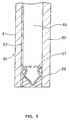
FIG. 5 is a sectional view showing an embodiment of a double-glazing
unit according to the present invention. In the double-glazing unit
shown in FIG. 5, a transparent layered product 60 in which a crystalline
coating film 63 is formed on a glass sheet 61 is positioned so that the coating
film 63 faces an air layer 66. In the transparent layered product, other
layers such as an undercoating film or the like may be formed, which is not
shown in the figure. Similarly in this case, as the crystalline coating film, a
conductive coating film is used. The peripheries of the transparent layered
product 60 and a glass sheet 69 are bonded with a sealant 68 via a spacer 67
containing a desiccant. The glass sheet 69 may be a transparent layered
product in which a crystalline coating film is formed.
The air layer 66 may be formed as a low pressure layer by
exhausting the inside air to reduce the pressure. When the pressure inside
the air layer 66 is reduced, the insulating effect or the like can be improved
further. When the low pressure layer is used, it is preferable that the
peripheries of the transparent layered product and the glass sheet are sealed
using, for example, low-melting-point glass instead of using the spacer 67
and the sealant 68. In this case, it is preferred to place a spacer in the low
pressure layer to maintain the space between the transparent layered
product and the glass sheet. Instead of the air layer 66, an inert gas layer
filled with an inert gas such as an argon gas or the like may be used.
The above-mentioned double-glazing unit can be used as window
glass for buildings with an improved thermal insulation property due to the
low emissivity of the conductive coating film. The double-glazing unit using
the transparent layered product also can be used as window glass with an
excellent electromagnetic shielding characteristic. Furthermore, it also can
be used as glass for a door of a refrigerated display case for shops. When it
is used for a door of a refrigerator, the transparent layered product is
positioned outside the refrigerator. When being used for an electromagnetic
shielding window or a refrigerator, the double-glazing unit shown in the
figure is further processed. For example, in the case of the former, a ground
wire is provided for maintaining the conductive coating film to have ground
potential. In the case of the latter, an electrode terminal is formed for
utilizing the double-glazing unit as a heating element by applying voltage to
the conductive coating film, and a wiring is provided for connecting the
electrode terminal and a power supply.
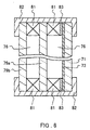
FIG. 6 is a sectional view of an embodiment of a glass door including
a transparent layered product according to the present invention. In this
glass door, a transparent layered product 71 and glass sheets 79a and 79b
are positioned with spaces via air layers 76 and spacers 81, which are
combined to form one body using a frame 82, thus forming a multiple-glazing
unit. Similarly in this multiple-glazing unit, a conductive crystalline
coating film 73 is formed on the side of the air layer 76. In order to allow
the coating film 73 to generate heat as a resistor, electrode terminals 83 are
positioned in contact with the coating film 73 at the both ends of the coating
film 73. This glass door has a function for preventing fogging caused by the
heat generation and is suitable as an opening/closing door of a display-type
refrigerator used frequently in shops for selling food stuffs or the like.
Examples
The present invention will be described further in detail using
examples as follows, but is not limited by the following examples.
In the following examples, respective films including a crystalline
coating film were deposited on a glass ribbon using a device for depositing a
film as described above. The number of coaters was changed suitably
depending on the number and thickness of layers to be stacked. Inside a
float bath, 98 vol.% nitrogen and 2 vol.% hydrogen were supplied so that the
pressure inside the bath was maintained to be slightly higher than that
outside the bath, and thus the inside of the bath was maintained under a
nonoxidative atmosphere. The temperature of the glass ribbon was
measured using a pyrometer at a location on a slightly upstream side from
the place where the films were formed.
In Examples 1 and 2, molten soda-lime silica glass (stained to have
a green color) with a flat glass composition was poured into the float bath
from a furnace, which then was formed into a glass ribbon with a thickness
of 6 mm. On the other hand, in Examples 3 to 13, molten soda-lime silica
glass (colorless) with a flat glass composition was poured into the float bath
from a furnace, which then was formed into a glass ribbon with a thickness
of 3 mm or 4 mm. In all of the above mentioned examples, the glass ribbon
was annealed in an annealing furnace and then was cut to have a
predetermined size on the further downstream side.
The following comparative examples were obtained by forming
transparent layered products having the same film structures as in
corresponding examples on a precut glass sheet by the CVD method. The
glass sheet used in the respective comparative examples had the same
thicknesses and compositions as those of the corresponding examples. The
specific film deposition method will be described as follows.
Manufacture of Heat-Reflecting Glass
Example 1
From a coater positioned on the furthest upstream side, a mixed gas
containing monosilane and nitrogen was supplied to deposit a silicon film
with a thickness of 25 nm on a glass ribbon. Then, from a coater on the
downstream side, a mixed gas containing monosilane, ethylene, oxygen, and
nitrogen was supplied to deposit a silicon oxide film with a thickness of 20
nm. Subsequently, from a coater on the further downstream side, a mixed
gas containing dimethyltin dichloride (vapor), oxygen, water vapor, nitrogen,
and helium was supplied to deposit a tin oxide film with a thickness of 12 nm
on the silicon oxide film. The temperature of the glass ribbon directly
before reaching the coater on the furthest upstream side was 680°C.
Comparative Example 1
A soda-lime glass sheet with a thickness of 6 mm that had been
precut to have a size of 450 mm × 450 mm was placed on a mesh belt and was
passed through a heating furnace to be heated up to about 600°C. While
this heated glass sheet was conveyed further, from a coater installed above a
glass carrier line, a mixed gas containing monosilane and nitrogen was
supplied to deposit a silicon film with a thickness of 25 nm on the glass sheet.
This glass sheet was annealed and then was placed on the mesh belt again
and was passed through a heating furnace to be heated up to about 600°C.
While this heated glass sheet was conveyed further, from a coater installed
above the glass carrier line, a mixed gas containing monosilane, oxygen and
nitrogen was supplied to deposit a silicon oxide film with a thickness of 20
nm on the silicon film. After being annealed, the glass sheet was placed on
the mesh belt again and was passed through a heating furnace to be heated
up to about 600°C. While this heated glass sheet was conveyed further,
from a coater installed above the glass carrier line, a mixed gas containing
monobutyltin trichloride (vapor), oxygen, water vapor, and nitrogen was
supplied to deposit a tin oxide film with a thickness of 12nm on the silicon
oxide film.
Example 2
As in Example 1, a silicon film with a thickness of 25 nm, a silicon
oxide film with a thickness of 20 nm, and a tin oxide film with a thickness of
12 nm were deposited sequentially on a glass ribbon. After that, from a
coater positioned on the further downstream side, a mixed gas containing
monosilane, ethylene, oxygen, and nitrogen was supplied to deposit a silicon
oxide film with a thickness of 1 nm on the tin oxide film. The temperature
of the glass ribbon directly before reaching the coater on the furthest
upstream side was 680°C.
Comparative Example 2
As in Comparative Example 1, a silicon film with a thickness of 25
nm, a silicon oxide film with a thickness of 20 nm, and a tin oxide film with a
thickness of about 12 nm were deposited sequentially on a glass sheet with a
thickness of 6 mm. After being annealed, this glass sheet was placed on a
mesh belt again and was passed through a heating furnace to be heated up to
about 600°C. While this heated glass sheet was conveyed further, from a
coater installed above a glass carrier line, a mixed gas containing monosilane,
oxygen, and nitrogen was supplied to deposit a silicon oxide film with a
thickness of 1 nm on the tin oxide film.
Manufacture of Substrate for Thin Film Photoelectric Conversion Device and
Formation of Amorphous Silicon Film on the Substrate
Example 3
From a coater positioned on the furthest upstream side, a mixed gas
containing monosilane, ethylene, oxygen, and nitrogen was supplied to
deposit a silicon oxide film with a thickness of 40 nm on a glass ribbon.
Subsequently, from a coater on the downstream side, a mixed gas containing
dimethyltin dichloride (vapor), oxygen, water vapor, nitrogen, helium, and
hydrogen fluoride was supplied to deposit a fluorine-containing tin oxide
(SnO2 : F) film with a thickness of 720 nm on the silicon oxide film. The
temperature of the glass ribbon directly before reaching the coater on the
furthest upstream side was 700°C.
On the SnO2 : F film on the glass sheet obtained by cutting the glass
ribbon, an amorphous silicon carbide layer (a p-type layer) with a thickness
of 10 nm was deposited using monosilane, methane, and diborane as raw
materials by the plasma CVD method.
Comparative Example 3
A soda-lime glass sheet with a thickness of 4 mm that had been
precut to have a size of 450 mm × 450 mm was placed on a mesh belt and was
passed through a heating furnace to be heated up to about 600°C. While
this heated glass sheet was conveyed further, from a coater installed above a
glass carrier line, a mixed gas containing monosilane, oxygen, and nitrogen
was supplied to deposit a silicon oxide film with a thickness of 25 nm on the
glass sheet. After being annealed, this glass sheet was placed on the mesh
belt again and was passed through a heating furnace to be heated up to
about 600°C. While this heated glass sheet was conveyed further, from a
coater installed above the glass carrier line, a mixed gas containing
monobutyltin trichloride (vapor), oxygen, water vapor, nitrogen and
trifluoroacetic acid was supplied to deposit a SnO2 : F film with a thickness of
720 nm on the silicon oxide film.
On the SnO2 : F film on the glass sheet, an amorphous silicon
carbide layer (a p-type layer) with a thickness of 10 nm was deposited using
monosilane, methane, and diborane as raw materials by the plasma CVD
method.
Example 4
From a coater on the furthest upstream side, a mixed gas containing
dimethyltin dichloride (vapor), oxygen, nitrogen, and helium was supplied to
deposit a tin oxide film with a thickness of 25 nm on a glass ribbon. Then,
from a coater on the downstream side, a mixed gas containing monosilane,
ethylene, oxygen, and nitrogen was supplied to deposit a silicon oxide film
with a thickness of 15 nm on the tin oxide film. Subsequently, from a coater
on the further downstream side, a mixed gas containing dimethyltin
dichloride (vapor), oxygen, water vapor, nitrogen, helium, and hydrogen
fluoride was supplied to deposit a SnO2 : F film with a thickness of 720 nm on
the silicon oxide film. The temperature of the glass ribbon directly before
reaching the coater on the furthest upstream side was 700°C.
On the SnO2 : F film on the glass sheet obtained by cutting the glass
ribbon, an amorphous silicon carbide layer (a p-type layer) with a thickness
of 10 nm was deposited using monosilane, methane, and diborane as raw
materials by the plasma CVD method. Subsequently, an amorphous silicon
layer (an i-type layer) with a thickness of 300 nm was stacked using
monosilane as a raw material by the same plasma CVD method.
Comparative Example 4
A soda-lime glass sheet with a thickness of 4 mm that had been
precut to have a size of 450 mm × 450 mm was placed on a mesh belt and was
passed through a heating furnace to be heated up to about 600°C. While
this heated glass sheet was conveyed further, from a coater installed above a
glass carrier line, a mixed gas containing dimethyltin dichloride (vapor),
oxygen, nitrogen, and helium was supplied to deposit a tin oxide film with a
thickness of 25 nm on the glass sheet. After being annealed, this glass
sheet was placed on the mesh belt again and was passed through a heating
furnace to be heated up to about 600°C. While this heated glass sheet was
conveyed further, from a coater installed above the glass carrier line, a mixed
gas containing monosilane, oxygen and nitrogen was supplied to deposit a
silicon oxide film with a thickness of 15 nm on the tin oxide film. After
being annealed, the glass sheet was placed on the mesh belt again and was
passed through a heating furnace to be heated up to about 600°C. While
this heated glass sheet was conveyed further, from a coater installed above
the glass carrier line, a mixed gas containing monobutyltin trichloride
(vapor), oxygen, water vapor, nitrogen, and trifluoroacetic acid was supplied
to deposit a SnO2 : F film with a thickness of 720 nm on the silicon oxide film.
On the SnO2 : F film on the glass sheet, an amorphous silicon
carbide layer (a p-type layer) with a thickness of 10 nm was deposited using
monosilane, methane, and diborane as raw materials by the plasma CVD
method. Subsequently, an amorphous silicon layer (an i-type layer) with a
thickness of 300 nm was stacked using monosilane as a raw material by the
same plasma CVD method.
Manufacture of Low-Emissivity Glass
Example 5
As in Example 4, a tin oxide film with a thickness of 25 nm, a silicon
oxide film with a thickness of 25 nm, and a SnO2 : F film with a thickness of
350 nm were deposited sequentially on a glass ribbon. The temperature of
the glass ribbon directly before reaching the coater on the furthest upstream
side was 650°C. The above-mentioned thickness of the SnO2 : F film is in a
preferable range for use as low-emissivity glass.
Comparative Example 5
As in Comparative Example 4, a tin oxide film with a thickness of 25
nm, a silicon oxide film with a thickness of 25 nm, and a SnO2 : F film with a
thickness of 350 nm were deposited sequentially on a glass sheet.
Manufacture of Electromagnetic Shielding Glass
Example 6
As in Example 4, a tin oxide film with a thickness of 35 nm, a silicon
oxide film with a thickness of 30 nm, and a SnO2 : F film with a thickness of
520 nm were deposited sequentially on a glass ribbon. The temperature of
the glass ribbon directly before reaching the coater on the furthest upstream
side was 680°C. The above-mentioned thickness of the SnO2 : F film is in a
preferable range for use as electromagnetic shielding glass.
Comparative Example 6
As in Comparative Example 4, a tin oxide film with a thickness of 35
nm, a silicon oxide film with a thickness of 30 nm, and a SnO2 : F film with a
thickness of 520 nm were deposited sequentially on a glass sheet.
Manufacture of Glass for Door of Refrigerator
Example 7
As in Example 4, a tin oxide film with a thickness of 45 nm, a silicon
oxide film with a thickness of 40 nm, and a SnO2 : F film with a thickness of
420 nm were deposited sequentially on a glass ribbon. The temperature of
the glass ribbon directly before reaching the coater on the furthest upstream
side was 680°C. The above-mentioned thickness of the SnO2 : F film is in a
preferable range for use as a glass door of a refrigerated display case.
Comparative Example 7
As in Comparative Example 4, a tin oxide film with a thickness of 45
nm, a silicon oxide film with a thickness of 40 nm, and a SnO2 : F film with a
thickness of 420 nm were deposited sequentially on a glass sheet.
Manufacture of Glass for Information Display Equipment
Example 8
As in Example 4, a tin oxide film with a thickness of 25 nm, a silicon
oxide film with a thickness of 20 nm, and a SnO2 : F film with a thickness of
270 nm were deposited sequentially on a glass ribbon. The temperature of
the glass ribbon directly before reaching the coater on the furthest upstream
side was 680°C. The above-mentioned thickness of the SnO2 : F film is in a
preferable range for use as glass for information display equipment.
Comparative Example 8
As in Comparative Example 4, a tin oxide film with a thickness of 25
nm, a silicon oxide film with a thickness of 20 nm, and a SnO2 : F film with a
thickness of 270 nm were deposited sequentially on a glass sheet.
Manufacture of Glass for Top Plate of Duplicator
Example 9
As in Example 3, a silicon oxide film with a thickness of 20 nm and a
SnO2 : F film with a thickness of 40 nm were deposited sequentially on a
glass ribbon. The temperature of the glass ribbon directly before reaching
the coater on the furthest upstream side was 680°C. The above-mentioned
thickness of the SnO2 : F film is in a preferable range for use as antistatic
glass used for a top plate of a duplicator or the like.
Comparative Example 9
As in Comparative Example 3, a silicon oxide film with a thickness
of 20 nm and a SnO2 : F film with a thickness of 40 nm were deposited
sequentially on a glass sheet.
Manufacture of Antifouling Glass
Example 10
From a coater on the furthest upstream side, a mixed gas containing
dimethyltin dichloride (vapor), oxygen, nitrogen, and helium was supplied to
deposit a tin oxide film with a thickness of 35 nm on a glass ribbon. Then,
from a coater on the downstream side, a mixed gas containing monosilane,
ethylene, oxygen, and nitrogen was supplied to deposit a silicon oxide film
with a thickness of 25 nm on the tin oxide film. Subsequently, from a coater
on the further downstream side, a mixed gas containing titanium
isopropoxide (vapor), oxygen, water vapor, nitrogen, helium, and
trifluoroacetic acid was supplied to deposit a titanium oxide film with a
thickness of 250 nm on the silicon oxide film. From a coater positioned on
the further downstream side, a mixed gas containing monosilane, ethylene,
oxygen, and nitrogen was supplied to deposit a silicon oxide film with a
thickness of 10 nm on the titanium oxide film. The temperature of the glass
ribbon directly before reaching the coater on the furthest upstream side was
700°C.
Comparative Example 10
A soda-lime glass sheet with a thickness of 4 mm that had been
precut to have a size of 450 mm × 450 mm was placed on a mesh belt and was
passed through a heating furnace to be heated up to about 600°C. While
this heated glass sheet was conveyed further, from a coater installed above a
glass carrier line, a mixed gas containing dimethyltin dichloride (vapor),
oxygen, nitrogen, and helium was supplied to deposit a tin oxide film with a
thickness of 35 nm on the glass sheet. After being annealed, this glass
sheet was placed on the mesh belt again and was passed though a heating
furnace to be heated up to about 600°C. While this heated glass sheet was
conveyed further, from a coater installed above the glass carrier line, a mixed
gas containing monosilane, oxygen and nitrogen was supplied to deposit a
silicon oxide film with a thickness of 25 nm on the tin oxide film. After
being annealed, the glass sheet was placed on the mesh belt again and was
passed through a heating furnace to be heated up to about 600°C. While
this heated glass sheet was conveyed further, from a coater installed above
the glass carrier line, a mixed gas containing titanium isopropoxide (vapor),
oxygen, water vapor, nitrogen, helium, and trifluoroacetic acid was supplied
to deposit a titanium oxide film with a thickness of 250 nm on the silicon
oxide film. After being annealed, this glass sheet was placed on the mesh
belt again and was passed through a heating furnace to be heated up to
about 600°C. While this heated glass sheet was conveyed further, from a
coater installed above the glass carrier line, a mixed gas containing
monosilane, oxygen, and nitrogen was supplied to deposit a silicon oxide film
with a thickness of 10 nm on the titanium oxide film.
Manufacture of Anti-Reflecting Glass
Example 11
From a coater on the furthest upstream side, a mixed gas containing
titanium isopropoxide (vapor), tetraethoxysilane (vapor), oxygen, water
vapor, nitrogen, helium, and trifluoroacetic acid was supplied to deposit a
titanium-silicon oxide film with a thickness of 130 nm on a glass ribbon.
Subsequently, from a coater on the downstream side, a mixed gas containing
monosilane, ethylene, oxygen, and nitrogen was supplied to deposit a silicon
oxide film with a thickness of 90 nm on the titanium-silicon oxide film. The
temperature of the glass ribbon directly before reaching the coater on the
furthest upstream side was 700°C.
Comparative Example 11
A soda-lime glass sheet with a thickness of 3 mm that had been
precut to have a size of 450 mm × 450 mm was placed on a mesh belt and was
passed through a heating furnace to be heated up to about 600°C. While
this heated glass sheet was conveyed further, from a coater installed above a
glass carrier line, a mixed gas containing titanium isopropoxide (vapor),
tetraethoxysilane (vapor), oxygen, water vapor, nitrogen, helium, and
trifluoroacetic acid was supplied to deposit a titanium-silicon oxide film with
a thickness of 130 nm on the glass sheet. After being annealed, this glass
sheet was placed on the mesh belt again and was passed through a heating
furnace to be heated up to about 600°C. While this heated glass sheet was
conveyed further, from a coater installed above the glass carrier line, a mixed
gas containing monosilane, oxygen and nitrogen was supplied to deposit a
silicon oxide film with a thickness of 90 nm on the titanium-silicon oxide
film.
Example 12
From a coater on the furthest upstream side, a mixed gas containing
SiH2Cl2, ethylene, oxygen, and nitrogen was supplied to deposit a silicon
oxide film with a thickness of 100 nm on a glass ribbon. The temperature of
the glass ribbon directly before reaching the coater on the furthest upstream
side was 710°C.
Comparative Example 12
A soda-lime glass sheet with a thickness of 3 mm that had been
precut to have a size of 450 mm × 450 mm was placed on a mesh belt and was
passed through a heating furnace to be heated up to about 600°C. While
this heated glass sheet was conveyed further, from a coater installed above a
glass carrier line, a mixed gas containing SiH2Cl2, ethylene, oxygen, and
nitrogen was supplied to deposit a silicon oxide film with a thickness of 100
nm on the glass sheet.
The coating film obtained according to Example 12 was observed by
an electron microscope. In the coating film, sodium chloride was contained
and many holes also were confirmed, which seemed to be produced due to the
dissociation of the sodium chloride. It is surmised that the sodium chloride
was produced by the reaction between sodium in the glass and chlorine in
the mixed gas. On the other hand, in the coating film obtained according to
Comparative Example 12, neither sodium chloride nor holes were found. It
is conceivable that the use of a material containing chlorine and a high film
formation temperature are required for the production of sodium chloride.
It was confirmed that the silicon oxide film was a substantially amorphous
film.
Manufacture of High-Reflectivity Glass
Example 13
From a coater on the furthest upstream side, a mixed gas containing
monosilane and nitrogen was supplied to deposit a silicon film with a
thickness of 30 nm on a glass ribbon. Then, from a coater on the
downstream side, a mixed gas containing monosilane, ethylene, oxygen, and
nitrogen was supplied to deposit a silicon oxide film with a thickness of 50
nm on the silicon film. Subsequently, from a coater on the further
downstream side, a mixed gas containing dimethyltin dichloride (vapor),
oxygen, water vapor, nitrogen, and helium was supplied to deposit a tin oxide
film with a thickness of about 90 nm on the silicon oxide film. The
temperature of the glass ribbon directly before reaching the coater on the
furthest upstream side was 680°C.
Comparative Example 13
A soda-lime glass sheet with a thickness of 3 mm that had been
precut to have a size of 450 mm × 450 mm was placed on a mesh belt and was
passed through a heating furnace to be heated up to about 600°C. While
this heated glass sheet was conveyed further, from a coater installed above a
glass carrier line, a mixed gas containing monosilane and nitrogen was
supplied to deposit a silicon film with a thickness of 30 nm on the glass sheet.
After being annealed, this glass sheet was placed on the mesh belt again and
was passed through a heating furnace to be heated up to about 600°C.
While this heated glass sheet was conveyed further, from a coater installed
above the glass carrier line, a mixed gas containing monosilane, ethylene,
oxygen, and nitrogen was supplied to deposit a silicon oxide film with a
thickness of 50 nm on the silicon film. After being annealed, the glass sheet,
was placed on the mesh belt again and was passed through a heating furnace
to be heated up to about 600°C. While this heated glass sheet was conveyed
further, from a coater installed above the glass carrier line, a mixed gas
containing dimethyltin dichloride (vapor), oxygen, water vapor, nitrogen, and
helium was supplied to deposit a tin oxide film with a thickness of 90 nm on
the silicon oxide film.
The reflectances and transmittances of samples obtained according
to the above-mentioned examples and comparative examples were measured
by a spectrophotometer, thus obtaining visible-light reflectances and visible-light
transmittances. Furthermore, with respect to respective thin films,
corresponding single-layer films with a smooth surface were produced, and
the wavelength distribution of the refractive index and extinction coefficient
of respective single-layer films was determined by measurement using a
spectral ellipsometer, which was used for the following optical calculation.
The thicknesses of respective transition layers were measured by an
interatomic force microscope to obtain rough values. After that, the
following optical calculation was carried out using the thickness of each
transition layer as a parameter, thus specifying the thickness of each
transition layer over a larger area.
It has been well known that if the refractive index and extinction
coefficient of respective films were given, the reflectance and transmittance,
further the visible-light reflectance and the visible-light transmittance of a
multilayered film, can be calculated by an optical calculation. Therefore,
the transition layers of respective coating films were divided in their
thickness direction, and refractive index distribution models were made by
presuming the refractive indexes of respective portions individually. Then,
a model most corresponding to the data obtained by the calculation was
picked out. Specifically, as shown in FIG. 3, the transition layer was
divided in the direction of its thickness (t2 - t1 : the principal plane of the
glass sheet was set to be 0) and the variation in refractive index (n1 - n2 :
wherein n1 denotes the refractive index of a medium (a thin film or air) on
the coating film, and n2 indicates the refractive index of the coating film) was
allocated to the respective divided portions. The transition layer was
divided into at least eight portions in its thickness direction to carry out the
allocation.
As a result, as in a typical example shown in FIG. 3, the refractive
index distribution in the transition layer in each example was able to be
better approximated to a model 22. From this, it is conceivable that the
actual refractive index distribution of each example is indicated by a curved
line such as a curved line 23. This curved line has a convex shape as a
whole and no point of inflection. On the other hand, the refractive index
distribution assumed from the model most approximated from the results of
the respective comparative examples was indicated by a straight line 21
pattern. The point (np, tp) on the curved line 23 and the point (nq, tq) on the
straight line 21 extending between the both ends (points (n1, t1) and (n2, t2))
of the transition layer have a relationship of tp > tq over the whole region of
the transition layer, if np = nq. In the respective examples described above,
the minimum value of (tp - tq) / (t2 - t1) was at least 0.05.
Tables 1 and 2 show the visible-light reflectance and the visible-light
transmittance measured with respect to the respective examples and
comparative examples, and the pattern of the variation in refractive index in
each transition layer obtained by the above-mentioned calculation. In every
example and comparative example, the ratio of the transition layer (to a
nontransition layer in the coating film in which the transition layer is
included) specified by the above was within a range between 10% and 30%.
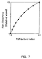
FIGs. 7 and 8 show the variations in refractive index of the
transition layers in Example 3 and Comparative Example 3, respectively.
| | Visible-Light Reflectance (%) | Visible-Light Transmittance (%) | Refractive Index Distribution |
| Example 1 | 41.7 | 31.9 | Convex Curve |
| Comparative Example 1 | 42.1 | 31.5 | Straight Line |
| Example 2 | 41.4 | 32.2 | Convex Curve |
| Comparative Example 2 | 42.2 | 31.4 | Straight Line |
| Example 3 | 24.9 | 67.4 | Convex Curve |
| Comparative Example 3 | 25.1 | 66.8 | Straight Line |
| Example 4 | 10.9 | - | Convex Curve |
| Comparative Example 4 | 11.1 | - | Straight Line |
| Example 5 | 10.3 | 85.4 | Convex Curve |
| Comparative Example 5 | 11.1 | 84.5 | Straight Line |
| Example 6 | 12.4 | 83.2 | Convex Curve |
| Comparative Example 6 | 13.2 | 82.4 | Straight Line |
| | Visible-Light Reflectance (%) | Visible-Light Transmittance(%) | Refractive Index Distribution |
| Example 7 | 11.9 | 84.4 | Convex Curve |
| Comparative Example 7 | 12.4 | 83.8 | Straight Line |
| Example 8 | 9.6 | 85.8 | Convex Curve |
| Comparative Example 8 | 10.1 | 86.4 | Straight Line |
| Example 9 | 9.3 | 90.1 | Convex Curve |
| Comparative Example 9 | 9.8 | 89.7 | Straight Line |
| Example 10 | 18.4 | 73.2 | Convex Curve |
| Comparative Example 10 | 19.2 | 72.4 | Straight Line |
| Example 11 | 6.9 | 92.4 | Convex Curve |
| Comparative Example 11 | 7.4 | 91.8 | Straight Line |
| Example 12 | 5.6 | 93.8 | Convex Curve |
| Comparative Example 12 | 7.1 | 91.4 | Straight Line |
| Example 13 | 72.4 | - | Convex Curve |
| Comparative Example 13 | 72.6 | - | Straight Line |
As shown in Tables 1 and 2, the respective cases were compared to
the corresponding cases using the same film structures, and it was confirmed
that the decrease in reflectance and the increase in transmittance in the
respective examples with the refractive index distribution indicated by a
convex curve were confirmed when compared to those in the comparative
examples with the refractive index distribution indicated by a straight line.
In Example 4 and Comparative Example 4, absorption by the amorphous
silicon layers was too great to measure the visible-light transmittance.
With respect to the transparent layered products obtained according
to Example 12 and Comparative Example 12, the spectral reflectance curves
were determined. As a result, the curve at the beginning on the short
wavelength side in the visible region in the example was more gentle than
that in the comparative example. Such flattening in the reflectance curve
was preferable for avoiding the coloring of reflected light, and also results in
the decrease in angular dependence of the reflected light color. In a
preferable embodiment of the present invention, such preferable effects also
can be obtained.
Manufacture of Photoelectric Conversion Device
Example 14
On the conductive film of the glass sheet with a conductive film
according to Example 3, an amorphous silicon photovoltaic unit was formed
by the plasma CVD method, thus obtaining a thin film photoelectric
conversion device. In the pin junction included in the amorphous silicon
photovoltaic unit, a p-type amorphous silicon carbide layer and an n-type
amorphous silicon layer were used and had thicknesses of 15 nm and 30 nm,
respectively. An intrinsic amorphous silicon layer (i-type) was formed by a
RF plasma CVD method. As film deposition conditions, a reaction gas of
silane, a pressure inside a reaction chamber of about 40 Pa, a RF power
density of 15 mW/cm2, and a film deposition temperature of 150°C were used.
An intrinsic amorphous silicon film deposited directly on a glass substrate to
have a thickness of 300 nm under the same film deposition conditions as
those described above had a dark conductivity of 5 × 10⁻¹⁰ S/cm. The
thickness of the intrinsic amorphous silicon layer was set to be 300 nm.
Finally, as a back electrode, an ITO film with a thickness of 80 nm and an Ag
film with a thickness of 300 nm were deposited on the amorphous silicon
photovoltaic unit by sputtering in this order.
The output characteristics of the thin film photoelectric conversion
device (with a photovoltaic area of 1 cm2) thus produced were measured
while light of AM1.5 (100mW/cm2) was irradiated as incident light. The
results included an open circuit voltage of 0.89V, a short-circuit current
density of 16.4 mA/cm2, a fill factor of 72.0%, and a conversion efficiency of
10.5 %. Further, an optical degradation test was carried out by irradiating
light of AM1.5 (100mW/cm2) at 48°C. After 550 hours irradiation, the
conversion efficiency was deteriorated up to 8.7%.
As described above, according to the present invention, a
transparent layered product with a light reflectance decreased by controlling
the variation in refractive index in a transition layer can be provided. As
described above, the present invention can exhibit the effects when a film is
formed to add various functions. In addition, the transparent layered
product of the present invention can be used as a glass article including
other members. For example, when the transparent layered product is used
in a photoelectric conversion device, the conversion efficiency can be
improved by reducing the reflection of incident light.