EP1056249A2 - Multicarrier receiver with noise detection and frequency control - Google Patents
Multicarrier receiver with noise detection and frequency control Download PDFInfo
- Publication number
- EP1056249A2 EP1056249A2 EP00304320A EP00304320A EP1056249A2 EP 1056249 A2 EP1056249 A2 EP 1056249A2 EP 00304320 A EP00304320 A EP 00304320A EP 00304320 A EP00304320 A EP 00304320A EP 1056249 A2 EP1056249 A2 EP 1056249A2
- Authority
- EP
- European Patent Office
- Prior art keywords
- signal
- frequency
- section
- sub
- noise
- Prior art date
- Legal status (The legal status is an assumption and is not a legal conclusion. Google has not performed a legal analysis and makes no representation as to the accuracy of the status listed.)
- Granted
Links
- 238000001514 detection method Methods 0.000 title claims description 39
- 239000000969 carrier Substances 0.000 claims abstract description 19
- 238000006243 chemical reaction Methods 0.000 claims abstract description 6
- 238000012937 correction Methods 0.000 abstract description 10
- 230000009466 transformation Effects 0.000 abstract description 7
- 238000000034 method Methods 0.000 description 49
- 230000008569 process Effects 0.000 description 46
- 230000001360 synchronised effect Effects 0.000 description 18
- 230000005540 biological transmission Effects 0.000 description 12
- 238000010586 diagram Methods 0.000 description 11
- 238000012545 processing Methods 0.000 description 10
- 230000008859 change Effects 0.000 description 3
- 230000007274 generation of a signal involved in cell-cell signaling Effects 0.000 description 3
- 230000010355 oscillation Effects 0.000 description 3
- 230000001629 suppression Effects 0.000 description 3
- 239000013078 crystal Substances 0.000 description 2
- 230000000694 effects Effects 0.000 description 2
- 238000004891 communication Methods 0.000 description 1
- 230000003247 decreasing effect Effects 0.000 description 1
- 238000011156 evaluation Methods 0.000 description 1
- 238000012854 evaluation process Methods 0.000 description 1
- 230000006872 improvement Effects 0.000 description 1
- 238000010295 mobile communication Methods 0.000 description 1
- 238000012986 modification Methods 0.000 description 1
- 230000004048 modification Effects 0.000 description 1
- 238000005070 sampling Methods 0.000 description 1
- 238000012546 transfer Methods 0.000 description 1
Images



Classifications
-
- H—ELECTRICITY
- H04—ELECTRIC COMMUNICATION TECHNIQUE
- H04L—TRANSMISSION OF DIGITAL INFORMATION, e.g. TELEGRAPHIC COMMUNICATION
- H04L27/00—Modulated-carrier systems
- H04L27/26—Systems using multi-frequency codes
- H04L27/2601—Multicarrier modulation systems
- H04L27/2647—Arrangements specific to the receiver only
- H04L27/2655—Synchronisation arrangements
- H04L27/2657—Carrier synchronisation
-
- H—ELECTRICITY
- H04—ELECTRIC COMMUNICATION TECHNIQUE
- H04L—TRANSMISSION OF DIGITAL INFORMATION, e.g. TELEGRAPHIC COMMUNICATION
- H04L27/00—Modulated-carrier systems
- H04L27/26—Systems using multi-frequency codes
- H04L27/2601—Multicarrier modulation systems
- H04L27/2647—Arrangements specific to the receiver only
- H04L27/2655—Synchronisation arrangements
- H04L27/2668—Details of algorithms
- H04L27/2673—Details of algorithms characterised by synchronisation parameters
- H04L27/2676—Blind, i.e. without using known symbols
Definitions
- the present invention relates to a receiving apparatus which receives an OFDM (Orthogonal Frequency Division Multiplex) modulated signal and, in particular, relates to a receiving apparatus which suppresses the influence due to noise components contained in the receiving signal to improve a carrier to noise ratio (CN ratio).
- OFDM Orthogonal Frequency Division Multiplex
- the OFDM modulation system In the communication field such as the mobile communication etc., the OFDM modulation system is applied which multiplexes the transmission information by the frequency division to make it possible to transmit the information with high quality and at a high frequency utilizing efficiency.
- an OFDM receiving apparatus which receives the modulated signal according to the OFDM modulation system.
- an antenna 1 receives an OFDM modulated radio signal.
- the high frequency signal thus received is frequency converted into an intermediate frequency signal IF by a front end including a high frequency amplifier 2, a mixer 3 and a local oscillator 10.
- the intermediate frequency signal IF is passed through a band pass filter 4 and amplified by an intermediate frequency amplifier 5 to a level capable of being signal processed.
- the signal thus amplified is supplied to a demodulating section formed by an analog-to-digital (A/D) converter 6, a demodulator 7, an OFDM demodulator 8 and a frame synchronous detector 12.
- A/D analog-to-digital
- An oscillator 11 is controlled by a system controller 13 in a manner that it generates predetermined timing clocks and supplies these clocks to the A/D converter 6, the demodulator 7 and the OFDM demodulator 8.
- the A/D converter 6 converts the aforesaid intermediate frequency signal IF into a digital signal on the basis of the timing clocks from the oscillator 11 and supplies the digital signal to the demodulator 7.
- the demodulator 7 detects the intermediate frequency signal IF in synchronism with the timing clocks from the oscillator 11 to generate an in-phase component signal (I component signal) and a quadrature component signal (Q component signal) as a base band signal.
- the frame synchronous detector 12 detects the frame synchronous signal from the signal IF having been A/D converted by the A/D converter 6 to make the OFDM demodulator 8 perform the demodulating process on the basis of the timing clocks from the oscillator 11.
- the demodulator 7 supplies the I component signal and the Q component signal to the OFDM demodulator 8.
- the OFDM demodulator 8 subjects the I component signal and the Q component signal to the fast Fourier transformation (FFT) process at the predetermined timings synchronous with the frame synchronous signal and further to the differential demodulation process thereby to generate a demodulated signal and outputs the signal.
- FFT fast Fourier transformation
- the demodulated signal is subjected to the error correction process and the decoding process, and the decoded signal is outputted to a signal processing circuit 9.
- the signal processing circuit 9 subjects the compressed signal contained in the decoded signal to the expansion process etc. to convert into an original audio band signal etc. and then outputs to a speaker etc.
- the method of removing such noises by using the band pass filter 4 is employed.
- the frequency interval of the respective sub-carriers (the frequency between the adjacent channels) is a small value of about 1KHz
- a band pass filter with quite steep frequency discrimination characteristics is required.
- the noise suppressing effect depends on the variance etc. of the frequency characteristics of the band pass filter 4
- an object of the present invention is to provide a receiving apparatus which can suppress the influence due to noises contained in a receiving signal thereby to improve a carrier to noise ratio (CN ratio).
- the invention is arranged in a manner that in a receiving apparatus for receiving an OFDM signal which is transmitted in a form of a frame having a no-signal portion and a data portion subjected to OFDM modulation by a plurality of sub-carriers, the receiving apparatus includes
- the frequency of the tuning signal (reference frequency signal) used at the time of frequency-converting the received OFDM modulation signal into the intermediate signal is finely adjusted within the interval of the sub-carrier frequencies.
- This fine adjustment of the frequency is performed in accordance with the noise component of the no-signal portion contained in the OFDM signal, for example.
- the frequency of the tuning signal is feedback-controlled in accordance with the noise component.
- the invention is arranged in a manner that the receiving apparatus further includes error rate detection section for detecting an error rate at a time of decoding data contained in the data portion, wherein
- the frequency of the tuning signal is finely adjusted in accordance with the error rate.
- the sub-carriers in the intermediate frequency signal are separated from the noise component on the frequency axis.
- the noise component can be suppressed.
- the CN ratio can be improved and the signal can be received with high quality.
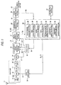
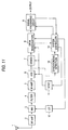
- Fig. 1 is a block diagram showing the arrangement of an OFDM receiving apparatus according to the embodiment.
- Fig. 2 is a diagram for explaining the frame format of a digital audio broadcasting (DAB) transmission signal in a DAB system to which the OFDM receiving apparatus of the invention can be applied.
- DAB digital audio broadcasting
- the frame format of the DAB transmission signal will be explained with reference to Fig. 2.
- the DAB transmission signal is formed by a frame having a synchronous channel, a fast information channel (FIC) succeeding thereto and a main service channel (MSC).
- the synchronous channel is formed by a null symbol having no signal and not being modulated, and a phase reference symbol including a reference signal as a phase reference for demodulation.
- the FIG channel is allotted mainly for the control data transmission.
- the MSC channel is allotted mainly for the transfer of main data such as audio data etc., for example.
- the DAB defines three transmission modes, that is , the mode 1 (for single frequency network) having the tuning frequency of 1.5GHz band and the frequency interval of the carrier wave of 1KHz, the mode 2 (for the ground broadcasting) having the tuning frequency of 39MHz band and the frequency interval of the carrier wave of 4KHz, the mode 3 (for the satellite broadcasting) having the tuning frequency of 200MHz band and the frequency interval of the carrier wave of 8KHz.
- the configuration of the OFDM receiving apparatus will be explained with reference to Fig. 1.
- the OFDM receiving apparatus is provided with a front end section which mixes a received signal obtained by receiving the DAB transmission signal by a receiving antenna 14 with a reference frequency signal LO from a local oscillator 24 thereby to frequency convert the received signal into an intermediate frequency signal S IF .
- the front end section is formed by a high frequency amplifier 15 which high-frequency amplifies the received signal, a mixer 16 which mixes a received signal S RF amplified by the high frequency amplifier 15 with the reference frequency signal LO thereby to frequency convert the received signal into an intermediate frequency signal, a band pass filter 17 which passes only the transmission band component (the frequency band component including all the sub-carriers) of the intermediate frequency signal, and an intermediate frequency amplifier 18 which amplifies the signal passed through the band pass filter 17 to a predetermined level suitable for the detection.
- the intermediate frequency amplifier 18 outputs the intermediate frequency signal S IF .
- the signal S IF having an intermediate frequency f IF which is the absolute value
- the frequency f 0 of the reference frequency signal LO is set to the frequency of (the tuning frequency + the intermediate frequency) when receiving the mode 3 of the DAB, and set to the frequency of (the tuning frequency - the intermediate frequency) when receiving the mode 1 or 2.
- the intermediate frequency f IF is set to 2.048MHz or 3.072MHz.
- the OFDM receiving apparatus is arranged to include an A/D converter 19, an IQ component signal generation section 20, a digital mixer / FFT calculation section 21, a differential demodulation section 22, an error correction section 23, an oscillator 25, a system controller 26 and an input / output section 27.
- the IQ component signal generation section 20, the digital mixer / FFT calculation section 21, the differential demodulation section 22, the error correction section 23 and the system controller 26 are formed by a digital signal processor (DSP).
- DSP digital signal processor
- the oscillator 25 generates synchronous clock signals C1 to C4 respectively having predetermined frequencies in accordance with a control signal Sc from the system controller 26.
- the A/D converter 19 converts the intermediate frequency signal S IF into the digital signal in synchronism with the clock signal C1 and outputs the digital signal.
- the sampling frequency of the clock signal C1 is set to 8.192MHz or 4.096MHz.
- the IQ component signal generation section 20 detects an in-phase component signal I and a quadrature component signal Q as a base band signal from the digital signal thus converted on the basis of the clock signal C2 (having the frequency of 4.096 MHz, for example), then separates these detected signals from the digital signal and outputs these signals thus separated.
- the digital mixer / FFT calculation section 21 subjects the in-phase component signal I and the quadrature component signal Q to the digital mixing process with the clock signal C4 of the local frequency synchronizing with the clock signal C1, then subjects the signal obtained from the mixing process to the fast Fourier transformation (FFT) process in synchronous with the clock signal C4 thereby to obtain signals S I , S Q on the frequency axis and outputs these signals. Further, the digital mixer / FFT calculation section supplies the signal obtained by the FFT process containing the signals S I , S Q to the system controller 26. In this respect, the FFT process is performed within one symbol in order to demodulate all data of the FIC channel and the MSC channel shown in Fig. 2.
- FFT fast Fourier transformation
- the differential demodulation section 22 subjects the signals S I , S Q to the differential demodulation thereby to generate and output a demodulated signal S1 as the demodulated output.
- the error correction section 23 subjects the demodulated signal S1 to the decoding process as well as the cancellation of the time interleave and the error correction process etc., to obtain a decoded signal S2 and outputs the decoded signal S2 to various kinds of signal processing sections, for example, a signal processing section etc. for subjecting the compressed signal contained in the decoded signal S2 to the expansion processing.
- the Viterbi decoding method is used for the decoding.
- the error correction section supplies data Se representing an error rate (bit error rate) detected by the aforesaid error correction to the system controller 26.
- the system controller 26 controls, based on tuning information designated by a user through the input / output section 27, the local oscillator 24 so as to set the frequency f 0 of the reference frequency signal LO thereof and the input / output section 27 so as to display various kinds of information such as a receiving channel etc. on a display section provided therein.
- the system controller 26 is provided with a synchronous detection section 28 and a null detection section 29 which are operated by executing system program set in advance, a noise detection section 30, a data detection section 31, a reference signal detection section 32, an error rate detection section 33 and a frequency control section 34. Further, the system controller is provided with a not-shown memory (storage section) for storing various kinds of data generated at the time of executing the system program.
- the null detection section 29 compares an amplitude value of a signal Sp outputted from the digital mixer / FFT calculation section 21 with a predetermined determination reference level and detects a portion of the signal smaller than the determination reference level as the null symbol shown in Fig. 2. To be more concrete, a portion of the sum of the square of the I component signal and the square of the Q component signal, that is, (I 2 + Q 2 ) smaller than the determination reference level is determined as the null symbol.
- the synchronous detection section 28 generates the frame synchronous signal based on the null symbol detected by the null detection section 29.
- the noise detection section 30 detects the sum (I 2 + Q 2 ) of the square of the I component signal and the square of the Q component signal as the power of the noise component mixed in the respective sub-carriers.
- the data detection section 31 and the reference signal detection section 32 detect FIC section and the MSC section shown in Fig. 2 in accordance with the timing of the frame synchronous signal detected by the synchronous detection section 28 and control the decoding process in the differential demodulation section 22 based on the detection result.
- the error rate detection section 33 compares the error rate data Se supplied from the error correction section 23 with a determination criterion. The error rate detection section determines that the receiving circumstance should be improved when a value of the error rate data Se is larger than the determination criterion ⁇ .
- the frequency control section 34 controls the frequency f 0 of the reference frequency signal LO so as to be set to a tunable frequency and automatically adjusts the respective synchronous clock signals C1 to C4 to the timings suitable for the demodulating process based on the tuning information designated by a user and the respective detection results of the synchronous detection section 28, the null detection section 29, the noise detection section 30, the data detection section 31, the reference signal detection section 32 and the error rate detection section 33.
- the frequency control section supplies control signals Sx, Sr to the local oscillator 24 thereby to have the local oscillator generate the reference frequency signal LO corresponding to the tuned channel designated by a user and finely adjust the frequency f 0 of the reference frequency signal LO in accordance with the power of the noise component detected by the noise detection section 30 and the determination result of the error rate detection section 33.
- the frequency control section supplies a control signal Sc to the oscillator 25, which in turn generates the synchronous clock signals C1 to C4 synchronous with the intermediate frequency signal S IF generated in accordance with the thus finely adjusted frequency f 0 of the reference frequency signal LO and automatically adjusts these clock signals to the timings suitable for the demodulating process.
- the local oscillator 24 is formed by a phase locked loop (PLL) including a phase comparator 35, a low pass filter 36 and a voltage control oscillator (VCO) 37, a control voltage generation circuit 39 for generating a control voltage Vx designated by the control signal Sx and a voltage control X'tal oscillator 38 for oscillating with a frequency according to the control voltage Vx.
- PLL phase locked loop
- VCO voltage control oscillator
- the voltage control X'tal oscillator 38 has such a property that the oscillation frequency thereof changes in accordance with the voltage applied thereto, as shown in Fig. 4. For example, the oscillation frequency becomes 18.432 MHz when the control voltage Vx is set at 2.5 volt. When the control voltage Vx is changed within a range of ⁇ 0.5 volt with reference to this frequency and 2.5 volt, the frequency deviation ⁇ f appears in a range of about ⁇ 100 ppm.
- Fig. 10 shows an example of setting values of the applied voltage for deviating the frequency by ⁇ f when the tuning frequency is at 1.5 GHz band and the intermediate frequency is 2.048 MHz. In this case, when the frequency deviation ⁇ f is 10 Hz, this frequency deviation ⁇ f corresponds to 0.0067 ppm of 1.5 GHz.
- VXO voltage control X' tal oscillator
- the voltage control X'tal oscillator 38 Since the control voltage Vx is set in accordance with the control signal Sx, the voltage control X'tal oscillator 38 generates a signal with a frequency fx which is proportional to the frequency f0 of the reference frequency signal LO to be finely adjusted. Further, since the frequency dividing ratio of a frequency dividing circuit 40 is set in accordance with the control signal Sr, the frequency dividing circuit subjects the frequency fx of the oscillation signal from the voltage control X'tal oscillator 38 to the frequency dividing process by the frequency dividing ratio corresponding to the tuned channel and supplies the frequency-divided signal to the PLL. Thus, the PLL generates the reference frequency signal LO with the frequency f0 which corresponds to a desired tuned channel and can be adjusted finely.
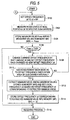
- the control signal Sx represents an offset value MF stored in the memory area (MF).
- the offset value MF is a value of the frequency deviation (hereinafter called an offset frequency) ⁇ f stored as history information when the user performed the receiving operation of the same channel at the previous tuning operation.
- the offset value MF is checked in order to finely adjust the reference frequency signal LO based on the previous offset frequency ⁇ f.
- the offset value MF of the tuned channel to be received for the first time is initially set at 0.
- step S100 when the offset value MF is 0, the offset frequency ⁇ f of the local oscillator 24 is set at 0 by the control signal Sx , so that the frequency f 0 of the reference frequency signal LO is not added with the offset frequency ⁇ f and hence set to the aforesaid standard local frequency of (the tuning frequency + the intermediate frequency) or (the tuning frequency - the intermediate frequency).
- the offset frequency ⁇ f of the local oscillator is set at MF, so that the frequency f 0 of the reference frequency signal LO is finely adjusted by adding the offset frequency ⁇ f obtained at the previous receiving operation thereto.
- the receiving operation is continued and the noise levels (power of the noise) at the null portions of the respective sub-carriers within the transmission band are measured (step 102). Then, the maximum value Pmax among the measured values of the respective noise levels is extracted and the maximum value Pmax is stored in the memory area (MRi) of the storage section in correspondence with the offset frequency ⁇ f (step S104).
- a symbol i depicts an address corresponding to the offset frequency ⁇ f.
- step S106 the maximum value Pmax is compared with a predetermined threshold value THD (step S106).
- Pmax ⁇ THD determination is "NO”
- step S116 the receiving process of step S116 is performed after executing the process of adjusting the offset frequency in steps S108 to S114.
- step S108 the local oscillator 24 is controlled by the control signal Sx thereby to change the offset frequency ⁇ f having been set therein by a predetermined shift amount ⁇ f and set the offset frequency thus changed as a new offset frequency ⁇ f. Further, a frequency obtained by shifting the standard local frequency by the new offset frequency ⁇ f is set as the frequency f 0 of the new reference frequency signal LO. The initial value of the offset frequency ⁇ f is set to 0.
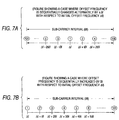
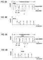
- the frequency ( ⁇ f + ⁇ f) which is higher by ⁇ f than the offset frequency ⁇ f having been set shown by a symbol 1 ⁇ in Fig. 7A is set as a new offset frequency ⁇ f shown by a symbol 2 ⁇ .
- the frequency f 0 of a new reference frequency signal LO is set based on the new offset frequency ⁇ f and the receiving process is continued.
- the receiving process is continued, and the noise levels (power of the noise) at the null portions of the respective sub-carriers within the transmission band are measured. Then, the maximum value Pmax among the measured values of the respective noise levels is extracted and the maximum value Pmax is stored in the memory area (MRi) of the storage section in correspondence with the offset frequency ⁇ f.
- a symbol i depicts an address corresponding to the offset frequency ⁇ f.
- step S110 it is determined whether the offset frequency ⁇ f has been changed based on the shift amount ⁇ f over the entire area of the sub-carrier interval Bf.
- the process returns to step S108 and the processes of steps S108 and S110 are repeated.
- the signal is received in accordance with the respective reference frequency signals LO which are obtained by sequentially shifting the offset frequency by integer numbers of times of the shift amount ⁇ f alternatively to the negative and positive directions. Then, the maximum noise power Pmax obtained at each time of shifting the offset frequency by the integer number of time of the shift amount ⁇ f is stored in the memory area (MRi) in correspondence with the offset frequency ⁇ f at this time.
- step S110 When it is confirmed in step S110 that the maximum noise powers Pmax have been measured in correspondence with all the offset frequencies ⁇ f over the entire area of the sub-carrier interval, the process returns to step S112, whereat the minimum noise power among all the maximum noise powers Pmax stored in the memory area (MRi) is extracted. In this case, when there are two or more minimum noise powers having the same value, one corresponding to the smallest offset value is extracted. Then, the frequency of the reference frequency signal LO is set again based on the offset frequency ⁇ f corresponding to the extracted minimum noise power. That is, the frequency of the reference frequency signal adjusted in this manner is the frequency capable of minimizing the influence due to the noise.
- the offset frequency ⁇ f corresponding to the extracted minimum noise power is stored in the memory area (MF) (step S114) and the receiving process is performed in step S116.
- the signal can be received with high quality. That is, as shown in Figs. 8A and 9A, when noise is mixed in the intermediate frequency signal S IF , the respective sub-carriers within the intermediate frequency signal S IF subjected to the frequency conversion based on the adjusted reference frequency signal LO are shifted to the frequencies most away from the noise as shown in Figs. 8B and 9B. In other words, the sub-carrier to be demodulated is separated from the frequency component of the noise.
- the digital mixer / FFT calculation section 21 performs the FFT process in synchronism with the intermediate frequency signal S IF thereby to suppress the noise, so that the signals S I , S Q of the in-phase component signal I and the quadrature component signal Q on the sub-carriers can be generated at high accuracy. As a result, the CN ratio can be improved and the signal can be received with high quality.
- the initial offset frequency ⁇ f may be set at 0 Hz (see mark 1 ⁇ ), and the offset frequency ⁇ f may be sequentially increased by a predetermined shift amount ⁇ f within the sub-carrier interval Bf (see marks 2 ⁇ 3 ⁇ 4 ⁇ ---).
- the initial offset frequency ⁇ f I may be set at 1 Hz, and the offset frequency ⁇ f may be sequentially decreased by a predetermined shift amount ⁇ f within the sub-carrier interval Bf.
- the present invention is not limited to the aforesaid shifting orders of the offset frequency.
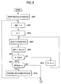
- the invention makes it possible to receive the signal with high quality by the processing shown in Fig. 6. That is, when a user designates a tuned channel, the processing shown in Fig. 6 is started before executing the processing shown in Fig. 5 (step S200).
- the error rate detection section 33 clears the memory area (ME) for storing the error rate data Se (step S202), then sets the count value K of a predetermined program counter to 1 (step S204), then in step S206 adds the error rate data Se transferred from the error correction section 23 to the value ME of the memory area (ME) and stores the result of the addition, that is, the sum in the memory area (ME) (step S208).
- step S210 it is determined whether the count value K reaches a value Kmax corresponding to a predetermined measuring time period.
- the count value of the counter is incremented by one (step S212), and the processing of steps S206 to S210 is repeated until the condition K > Kmax is satisfied.
- the added value ME of the error rate thus stored in the memory area (ME) within the predetermined measuring time period is divided by the value Kmax corresponding to the predetermined measuring time period thereby to obtain a time average value (ME / Kmax) of the error rate, and the time average value of the error rate is compared with the determination criterion ⁇ (step S214).
- the determination is made that the signal can be received without being influenced by noise, and the receiving process is continued based on the reference frequency signal LO set at the standard local frequency (step S216).
- the evaluation of the error rate is repeated in steps S202 to S214. In other words, the receiving operation is performed while evaluating the occurrence of the increase of the error rate at every lapse of the predetermined measuring time period.
- step S214 when it is determined in step S214 that the time average value of the error rate satisfies the condition of ME / Kmax ⁇ ⁇ (in the case of "NO"), the determination is made that the received signal is influenced by noise, then the process proceeds to step S100 of Fig. 5 and the aforesaid frequency adjusting process of the reference frequency signal LO is performed.
- step S100 As shown by a dotted line in Fig. 6, together with the continuation of the receiving process in step S216, the frequency adjusting process from step S100 may be started.
- the evaluating process of the error rate may be performed in the signal receiving process after the frequency adjusting process performed beforehand, or the error rate evaluating process and the frequency adjusting process may be combined in various manner. Further, the frequency adjusting process may be performed in accordance with the average value of the error rate detected by the error rate detection section 33.
- the frequency interval between the sub-carrier and the noise component is made larger by finely adjusting the frequency of the reference frequency signal LO shown in Fig. 1 and the noise component is suppressed through the FFT processing, the signal can be received with high quality.
- the invention intends to perform the demodulation process and the noise component suppression process simultaneously at the time of performing the FFT process. That is, the invention obtains the noise suppression effect by effectively utilizing such a feature that the OFDM modulation including the DAB is the discrete multi-carrier modulation. Thus, the invention does not require a particular noise removing circuit.
- the frequency of the reference frequency signal LO can be finely adjusted with high accuracy by utilizing the local oscillator 24 arranged as shown in Fig. 3.
- the frequency of the reference frequency signal LO can be adjusted with high accuracy to the frequencies capable of suppressing noise. Further, it becomes possible to miniaturize the receiving apparatus.
- the arrangement of the local oscillator 24 shown in Fig. 3 is an example, and a similar oscillator capable of changing the frequency may be employed therefore.
- the receiving apparatus is arranged in a manner that the noise component contained in the no-signal portion is detected as the noise component contained in the signal of the sub-carrier frequencies, and the intermediate frequency is deviated within the interval of the sub-carrier frequencies in accordance with the noise component contained in the no-signal portion.
- the sub-carriers in the intermediate frequency signal can be separated from the noise component on the frequency axis, and further the noise component can be suppressed when performing the Fourier transformation for the demodulation,.
- the CN ratio can be improved and the signal can be received with high quality.
- the invention is arranged in a manner that the receiving apparatus further includes error rate detection section for detecting an error rate at a time of decoding data, and the intermediate frequency is deviated within the interval of the sub-carrier frequencies in accordance with the noise component contained in the no-signal portion and the error rate.
- the sub-carriers in the intermediate frequency signal can be separated from the noise component on the frequency axis, and further the noise component can be suppressed when performing the Fourier transformation for the demodulation.
- the CN ratio can be improved and the signal can be received with high quality.
Landscapes
- Engineering & Computer Science (AREA)
- Computer Networks & Wireless Communication (AREA)
- Signal Processing (AREA)
- Noise Elimination (AREA)
Abstract
Description
Claims (4)
- A receiving apparatus for receiving an OFDM signal which is transmitted in a form of a frame having a no-signal portion and a data portion subjected to OFDM modulation by a plurality of sub-carriers,said receiving apparatus comprising:frequency conversion section for converting a tuned signal into an intermediate frequency signal;noise detection section for detecting a noise component contained in said no-signal portion as a noise component contained in a signal of the sub-carrier frequencies; andfrequency deviation section for deviating the intermediate frequency within an interval of the sub-carrier frequencies in accordance with the noise component contained in said no-signal portion detected by said noise detection section.
- The receiving apparatus according to claim 1, further comprising:error rate detection section for detecting an error rate at a time of decoding data contained in said data portion, whereinsaid frequency deviation section deviates the intermediate frequency within the interval of the sub-carrier frequencies in accordance with the noise component contained in said no-signal portion detected by said noise detection section and the error rate thus detected.
- The receiving apparatus according to claim 2, whereinsaid frequency deviation section deviates the intermediate frequency within the interval of the sub-carrier frequencies in accordance with the noise component contained in said no-signal portion detected by said noise detection section, when the detected error rate exceeds a preset threshold value.
- The receiving apparatus according to one of claims 1 to 3, further comprising:storage section for storing history information of a frequency deviation value set by said frequency deviation section, whereinsaid frequency deviation section sets the frequency deviation value stored in said storage section as an initial value, when a same channel is selected, and deviates the intermediate frequency within the interval of the sub-carrier frequencies with reference to the initial value.
Applications Claiming Priority (2)
| Application Number | Priority Date | Filing Date | Title |
|---|---|---|---|
| JP14860999 | 1999-05-27 | ||
| JP14860999A JP3675670B2 (en) | 1999-05-27 | 1999-05-27 | Receiver |
Publications (3)
| Publication Number | Publication Date |
|---|---|
| EP1056249A2 true EP1056249A2 (en) | 2000-11-29 |
| EP1056249A3 EP1056249A3 (en) | 2002-11-13 |
| EP1056249B1 EP1056249B1 (en) | 2004-11-10 |
Family
ID=15456615
Family Applications (1)
| Application Number | Title | Priority Date | Filing Date |
|---|---|---|---|
| EP00304320A Expired - Lifetime EP1056249B1 (en) | 1999-05-27 | 2000-05-22 | Multicarrier receiver with noise detection and frequency control |
Country Status (4)
| Country | Link |
|---|---|
| US (1) | US6744828B1 (en) |
| EP (1) | EP1056249B1 (en) |
| JP (1) | JP3675670B2 (en) |
| DE (1) | DE60015644T2 (en) |
Cited By (3)
| Publication number | Priority date | Publication date | Assignee | Title |
|---|---|---|---|---|
| KR100344693B1 (en) * | 2000-09-29 | 2002-07-25 | 주식회사 케이티프리텔 | AFC for the muti-carrier CDMA system and method for the compensating of frequency error |
| WO2005096582A1 (en) * | 2004-03-31 | 2005-10-13 | Koninklijke Philips Electronics N.V. | Receiver for a multi-carrier signal |
| WO2007014869A1 (en) * | 2005-08-03 | 2007-02-08 | Robert Bosch Gmbh | Radio receiving device |
Families Citing this family (31)
| Publication number | Priority date | Publication date | Assignee | Title |
|---|---|---|---|---|
| EP1170860A1 (en) * | 2000-06-27 | 2002-01-09 | Nortel Matra Cellular | Improved multi-carrier receiver for radio telecommunications network |
| KR100333818B1 (en) * | 2000-08-16 | 2002-04-26 | 윤종용 | Apparatus for detecting mode by using null symbols in digital audio receiver and method thereof |
| JP3776716B2 (en) * | 2000-11-17 | 2006-05-17 | 株式会社東芝 | Orthogonal frequency division multiplex transmission signal receiver |
| JP3385266B2 (en) | 2000-11-27 | 2003-03-10 | 富士通株式会社 | Noise removal method and apparatus |
| EP1341332A4 (en) | 2000-12-05 | 2005-03-30 | Fujitsu Ltd | APPARATUS AND METHOD FOR DATA TRANSMISSION |
| JP4548954B2 (en) * | 2001-03-09 | 2010-09-22 | 株式会社日立国際電気 | Interference signal canceller |
| JP4171261B2 (en) | 2001-08-27 | 2008-10-22 | 松下電器産業株式会社 | Wireless communication apparatus and wireless communication method |
| EP1300956A1 (en) * | 2001-10-02 | 2003-04-09 | Matsushita Electric Industrial Co., Ltd. | Receiving apparatus |
| US7269125B2 (en) * | 2001-12-26 | 2007-09-11 | Xm Satellite Radio, Inc. | Method and apparatus for timing recovery in an OFDM system |
| US7116731B2 (en) * | 2002-06-03 | 2006-10-03 | Vixs, Inc. | Method and apparatus for adjusting symbol timing and/or symbol positioning of a receive burst of data within a radio receiver |
| JP4154229B2 (en) * | 2002-12-27 | 2008-09-24 | 富士通株式会社 | Adaptive array antenna controller |
| EP1775770A4 (en) * | 2004-07-29 | 2013-01-02 | Panasonic Corp | RADIO TRANSMISSION DEVICE, RADIO RECEIVING DEVICE, RADIO TRANSMITTING METHOD, AND RADIO RECEIVING METHOD |
| JP4611182B2 (en) * | 2005-02-16 | 2011-01-12 | パナソニック株式会社 | Wireless terminal apparatus and communication method switching method |
| US7675369B2 (en) * | 2006-06-12 | 2010-03-09 | Honeywell International Inc. | Frequency hopping oscillator circuit |
| JP2008177842A (en) * | 2007-01-18 | 2008-07-31 | Mitsubishi Electric Corp | Reception device, transmission device, and communication system |
| KR100897769B1 (en) * | 2007-01-24 | 2009-05-15 | 삼성전자주식회사 | Channel state information estimation method and apparatus |
| JP4845838B2 (en) * | 2007-09-07 | 2011-12-28 | オンセミコンダクター・トレーディング・リミテッド | Noise suppression device |
| JP4664961B2 (en) * | 2007-12-13 | 2011-04-06 | 富士通株式会社 | Adaptive array antenna system |
| EP2117192B1 (en) * | 2008-05-09 | 2011-04-06 | Telefonaktiebolaget Lm Ericsson (publ) | Radio-receiver circuit |
| CN101355407A (en) * | 2008-09-26 | 2009-01-28 | 北京新岸线移动多媒体技术有限公司 | Receiver for ground mobile multimedia broadcast, receiving apparatus and method |
| KR100969665B1 (en) * | 2008-11-18 | 2010-07-14 | 주식회사 텔레칩스 | Apparatus and method for improving reception performance of OPDM communication system |
| KR101471678B1 (en) * | 2009-03-03 | 2014-12-11 | 에릭슨 엘지 주식회사 | Apparatus and method for estimating noise power in an LTE system |
| US8224279B2 (en) | 2009-12-18 | 2012-07-17 | Silicon Laboratories, Inc. | Radio frequency (RF) receiver with dynamic frequency planning and method therefor |
| US8874060B2 (en) * | 2009-12-18 | 2014-10-28 | Silicon Laboratories Inc. | Radio frequency (RF) receiver with frequency planning and method therefor |
| US20110217918A1 (en) * | 2010-03-05 | 2011-09-08 | Nxp B.V. | Device and method for jammer resistance in broadband receivers |
| JP5595883B2 (en) * | 2010-11-29 | 2014-09-24 | 株式会社東芝 | Wireless communication device |
| CN104135296B (en) * | 2014-07-12 | 2017-03-15 | 无锡中星微电子有限公司 | Adjustable mean frequency wireless receiver and bluetooth module |
| US11487871B2 (en) * | 2015-01-31 | 2022-11-01 | San Diego Gas & Electric Company | Methods and systems for detecting and defending against invalid time signals |
| KR102403368B1 (en) * | 2015-02-24 | 2022-05-30 | 삼성전자주식회사 | Phase looked loop using received signal |
| JP7736608B2 (en) * | 2022-03-22 | 2025-09-09 | パナソニックオートモーティブシステムズ株式会社 | Signal processing device and signal processing method |
| US12417709B2 (en) * | 2023-04-17 | 2025-09-16 | Dedrone Holdings, Inc. | Signal generation systems and methods for using same |
Family Cites Families (11)
| Publication number | Priority date | Publication date | Assignee | Title |
|---|---|---|---|---|
| FR2721778B1 (en) * | 1994-06-23 | 1996-09-06 | France Telecom | Method for estimating a residual phase error on the samples of a demodulated digital signal, and corresponding correction method. |
| JP3130752B2 (en) * | 1995-02-24 | 2001-01-31 | 株式会社東芝 | OFDM transmission receiving method and transmitting / receiving apparatus |
| JP3079950B2 (en) * | 1995-06-20 | 2000-08-21 | 松下電器産業株式会社 | Receiving apparatus and transmission method for orthogonal frequency division multiplex modulation signal |
| GB9521739D0 (en) * | 1995-10-24 | 1996-01-03 | Nat Transcommunications Ltd | Decoding carriers encoded using orthogonal frequency division multiplexing |
| DE69711957T2 (en) * | 1996-02-02 | 2002-09-19 | Deutsche Thomson-Brandt Gmbh | Method and device for receiving multicarrier signals |
| JP3549361B2 (en) * | 1997-05-13 | 2004-08-04 | 三菱電機株式会社 | Digital audio broadcasting receiver |
| JPH10313286A (en) * | 1997-05-13 | 1998-11-24 | Sony Corp | Receiver |
| US6058101A (en) * | 1997-06-11 | 2000-05-02 | Industrial Technology Research Institute | Synchronization method and system for a digital receiver |
| FR2768278B1 (en) * | 1997-09-11 | 1999-11-26 | France Telecom | PROCESS FOR ESTIMATING A PARASITIC PHASE OFFSET ON RECEPTION OF A MULTI-PORTABLE SIGNAL, AND CORRESPONDING RECEIVER |
| KR100252971B1 (en) * | 1998-02-25 | 2000-04-15 | 구자홍 | Automatic frequency control method of digital broadcasting receiver |
| DE69838787T2 (en) * | 1998-10-30 | 2008-10-30 | Fujitsu Ten Ltd., Kobe | Frequency correction in an OFDM (Orthogonal Frequency Division Multiplexing) receiver |
-
1999
- 1999-05-27 JP JP14860999A patent/JP3675670B2/en not_active Expired - Fee Related
-
2000
- 2000-05-22 EP EP00304320A patent/EP1056249B1/en not_active Expired - Lifetime
- 2000-05-22 DE DE60015644T patent/DE60015644T2/en not_active Expired - Fee Related
- 2000-05-23 US US09/577,360 patent/US6744828B1/en not_active Expired - Fee Related
Cited By (4)
| Publication number | Priority date | Publication date | Assignee | Title |
|---|---|---|---|---|
| KR100344693B1 (en) * | 2000-09-29 | 2002-07-25 | 주식회사 케이티프리텔 | AFC for the muti-carrier CDMA system and method for the compensating of frequency error |
| WO2005096582A1 (en) * | 2004-03-31 | 2005-10-13 | Koninklijke Philips Electronics N.V. | Receiver for a multi-carrier signal |
| US7650129B2 (en) | 2004-03-31 | 2010-01-19 | Nxp B.V. | Receiver for a multi-carrier signal |
| WO2007014869A1 (en) * | 2005-08-03 | 2007-02-08 | Robert Bosch Gmbh | Radio receiving device |
Also Published As
| Publication number | Publication date |
|---|---|
| EP1056249B1 (en) | 2004-11-10 |
| DE60015644T2 (en) | 2005-03-31 |
| JP2000341241A (en) | 2000-12-08 |
| JP3675670B2 (en) | 2005-07-27 |
| US6744828B1 (en) | 2004-06-01 |
| EP1056249A3 (en) | 2002-11-13 |
| DE60015644D1 (en) | 2004-12-16 |
Similar Documents
| Publication | Publication Date | Title |
|---|---|---|
| EP1056249B1 (en) | Multicarrier receiver with noise detection and frequency control | |
| US6219333B1 (en) | Method and apparatus for synchronizing a carrier frequency of an orthogonal frequency division multiplexing transmission system | |
| US7024172B1 (en) | Direct conversion receiver using a dithered local oscillator to mitigate adjacent channel coherent interference | |
| KR100242400B1 (en) | System for broadcasting and receiving digital data, receiver and transsmitter for use in such system | |
| US6907089B2 (en) | Digital demodulation and applications thereof | |
| US20100086081A1 (en) | Modulation device and demodulation device | |
| JPH10285135A (en) | Frequency controller and method, receiver and communication equipment | |
| KR100434006B1 (en) | A satellite receiver for digital broadcasting system | |
| US5388125A (en) | Frequency converter circuit with improved intermediate frequency stability | |
| US6862297B1 (en) | Wide range frequency offset estimation in OFDM systems | |
| US8254864B1 (en) | Decreasing user equipment measurement time | |
| KR19990023384A (en) | Digital Broadcast Receiver | |
| JP2000013358A (en) | Agc circuit and its control method | |
| JPH07250115A (en) | Digital data receiver | |
| US8731084B2 (en) | Multi-carrier communication apparatus | |
| KR19990060480A (en) | Digital residual sideband demodulation device | |
| EP0944213A2 (en) | Digital broadcast receiver | |
| JP3656797B2 (en) | Digital broadcast receiver | |
| JP3586084B2 (en) | Frequency control device, receiving device, and communication device | |
| JP3134801B2 (en) | Shared receiver | |
| JPH10209999A (en) | Automatic frequency control system | |
| JPH05336017A (en) | Receiver in frequency division multiple access communication system | |
| WO2005048552A1 (en) | Methods and apparatuses for dc offset estimation in ofdm systems | |
| JP2005026891A (en) | Frequency synthesizer, tuner and receiver | |
| KR950007090B1 (en) | Spread Spectrum Code Division Multiple Access Receiver |
Legal Events
| Date | Code | Title | Description |
|---|---|---|---|
| PUAI | Public reference made under article 153(3) epc to a published international application that has entered the european phase |
Free format text: ORIGINAL CODE: 0009012 |
|
| AK | Designated contracting states |
Kind code of ref document: A2 Designated state(s): AT BE CH CY DE DK ES FI FR GB GR IE IT LI LU MC NL PT SE |
|
| AX | Request for extension of the european patent |
Free format text: AL;LT;LV;MK;RO;SI |
|
| PUAL | Search report despatched |
Free format text: ORIGINAL CODE: 0009013 |
|
| AK | Designated contracting states |
Kind code of ref document: A3 Designated state(s): AT BE CH CY DE DK ES FI FR GB GR IE IT LI LU MC NL PT SE |
|
| AX | Request for extension of the european patent |
Free format text: AL;LT;LV;MK;RO;SI |
|
| 17P | Request for examination filed |
Effective date: 20030414 |
|
| AKX | Designation fees paid |
Designated state(s): DE FR GB |
|
| 17Q | First examination report despatched |
Effective date: 20030710 |
|
| GRAP | Despatch of communication of intention to grant a patent |
Free format text: ORIGINAL CODE: EPIDOSNIGR1 |
|
| GRAS | Grant fee paid |
Free format text: ORIGINAL CODE: EPIDOSNIGR3 |
|
| GRAA | (expected) grant |
Free format text: ORIGINAL CODE: 0009210 |
|
| AK | Designated contracting states |
Kind code of ref document: B1 Designated state(s): DE FR GB |
|
| REG | Reference to a national code |
Ref country code: GB Ref legal event code: FG4D |
|
| REG | Reference to a national code |
Ref country code: IE Ref legal event code: FG4D |
|
| REF | Corresponds to: |
Ref document number: 60015644 Country of ref document: DE Date of ref document: 20041216 Kind code of ref document: P |
|
| PLBE | No opposition filed within time limit |
Free format text: ORIGINAL CODE: 0009261 |
|
| STAA | Information on the status of an ep patent application or granted ep patent |
Free format text: STATUS: NO OPPOSITION FILED WITHIN TIME LIMIT |
|
| ET | Fr: translation filed | ||
| 26N | No opposition filed |
Effective date: 20050811 |
|
| PGFP | Annual fee paid to national office [announced via postgrant information from national office to epo] |
Ref country code: DE Payment date: 20070517 Year of fee payment: 8 |
|
| PGFP | Annual fee paid to national office [announced via postgrant information from national office to epo] |
Ref country code: GB Payment date: 20070516 Year of fee payment: 8 |
|
| PGFP | Annual fee paid to national office [announced via postgrant information from national office to epo] |
Ref country code: FR Payment date: 20070510 Year of fee payment: 8 |
|
| GBPC | Gb: european patent ceased through non-payment of renewal fee |
Effective date: 20080522 |
|
| REG | Reference to a national code |
Ref country code: FR Ref legal event code: ST Effective date: 20090119 |
|
| PG25 | Lapsed in a contracting state [announced via postgrant information from national office to epo] |
Ref country code: FR Free format text: LAPSE BECAUSE OF NON-PAYMENT OF DUE FEES Effective date: 20080602 Ref country code: DE Free format text: LAPSE BECAUSE OF NON-PAYMENT OF DUE FEES Effective date: 20081202 |
|
| PG25 | Lapsed in a contracting state [announced via postgrant information from national office to epo] |
Ref country code: GB Free format text: LAPSE BECAUSE OF NON-PAYMENT OF DUE FEES Effective date: 20080522 |