EP1056205A2 - Semiconductor apparatus - Google Patents
Semiconductor apparatus Download PDFInfo
- Publication number
- EP1056205A2 EP1056205A2 EP00304324A EP00304324A EP1056205A2 EP 1056205 A2 EP1056205 A2 EP 1056205A2 EP 00304324 A EP00304324 A EP 00304324A EP 00304324 A EP00304324 A EP 00304324A EP 1056205 A2 EP1056205 A2 EP 1056205A2
- Authority
- EP
- European Patent Office
- Prior art keywords
- semiconductor
- anomaly
- inverter
- alarm signal
- switching devices
- Prior art date
- Legal status (The legal status is an assumption and is not a legal conclusion. Google has not performed a legal analysis and makes no representation as to the accuracy of the status listed.)
- Granted
Links
Images


Classifications
-
- H—ELECTRICITY
- H02—GENERATION; CONVERSION OR DISTRIBUTION OF ELECTRIC POWER
- H02M—APPARATUS FOR CONVERSION BETWEEN AC AND AC, BETWEEN AC AND DC, OR BETWEEN DC AND DC, AND FOR USE WITH MAINS OR SIMILAR POWER SUPPLY SYSTEMS; CONVERSION OF DC OR AC INPUT POWER INTO SURGE OUTPUT POWER; CONTROL OR REGULATION THEREOF
- H02M1/00—Details of apparatus for conversion
- H02M1/32—Means for protecting converters other than automatic disconnection
-
- H—ELECTRICITY
- H02—GENERATION; CONVERSION OR DISTRIBUTION OF ELECTRIC POWER
- H02M—APPARATUS FOR CONVERSION BETWEEN AC AND AC, BETWEEN AC AND DC, OR BETWEEN DC AND DC, AND FOR USE WITH MAINS OR SIMILAR POWER SUPPLY SYSTEMS; CONVERSION OF DC OR AC INPUT POWER INTO SURGE OUTPUT POWER; CONTROL OR REGULATION THEREOF
- H02M7/00—Conversion of AC power input into DC power output; Conversion of DC power input into AC power output
- H02M7/42—Conversion of DC power input into AC power output without possibility of reversal
- H02M7/44—Conversion of DC power input into AC power output without possibility of reversal by static converters
- H02M7/48—Conversion of DC power input into AC power output without possibility of reversal by static converters using discharge tubes with control electrode or semiconductor devices with control electrode
- H02M7/53—Conversion of DC power input into AC power output without possibility of reversal by static converters using discharge tubes with control electrode or semiconductor devices with control electrode using devices of a triode or transistor type requiring continuous application of a control signal
- H02M7/537—Conversion of DC power input into AC power output without possibility of reversal by static converters using discharge tubes with control electrode or semiconductor devices with control electrode using devices of a triode or transistor type requiring continuous application of a control signal using semiconductor devices only, e.g. single switched pulse inverters
- H02M7/5387—Conversion of DC power input into AC power output without possibility of reversal by static converters using discharge tubes with control electrode or semiconductor devices with control electrode using devices of a triode or transistor type requiring continuous application of a control signal using semiconductor devices only, e.g. single switched pulse inverters in a bridge configuration
- H02M7/53871—Conversion of DC power input into AC power output without possibility of reversal by static converters using discharge tubes with control electrode or semiconductor devices with control electrode using devices of a triode or transistor type requiring continuous application of a control signal using semiconductor devices only, e.g. single switched pulse inverters in a bridge configuration with automatic control of output voltage or current
- H02M7/53875—Conversion of DC power input into AC power output without possibility of reversal by static converters using discharge tubes with control electrode or semiconductor devices with control electrode using devices of a triode or transistor type requiring continuous application of a control signal using semiconductor devices only, e.g. single switched pulse inverters in a bridge configuration with automatic control of output voltage or current with analogue control of three-phase output
-
- H—ELECTRICITY
- H03—ELECTRONIC CIRCUITRY
- H03K—PULSE TECHNIQUE
- H03K17/00—Electronic switching or gating, i.e. not by contact-making and –breaking
- H03K17/08—Modifications for protecting switching circuit against overcurrent or overvoltage
- H03K17/082—Modifications for protecting switching circuit against overcurrent or overvoltage by feedback from the output to the control circuit
- H03K17/0828—Modifications for protecting switching circuit against overcurrent or overvoltage by feedback from the output to the control circuit in composite switches
-
- H—ELECTRICITY
- H03—ELECTRONIC CIRCUITRY
- H03K—PULSE TECHNIQUE
- H03K17/00—Electronic switching or gating, i.e. not by contact-making and –breaking
- H03K17/08—Modifications for protecting switching circuit against overcurrent or overvoltage
- H03K2017/0806—Modifications for protecting switching circuit against overcurrent or overvoltage against excessive temperature
Definitions
- the present invention relates to a semiconductor apparatus incorporated in a power converting apparatus such as an inverter for variably controlling the speed of a motor. More specifically, the present invention relates to a so-called intelligent power module (hereinafter referred to as an "IPM") that incorporates semiconductor switching devices for power conversion, driver circuits for driving the respective semiconductor switching devices and various protection circuits in a package.
- IPM intelligent power module
- FIG. 6 is a block diagram showing the main portion of a conventional inverter for variably controlling the speed of a motor including an intelligent power module (IPM).
- IPM 01 an intelligent power module
- main DC power supply 02 formed of a not shown rectifier circuit in a main control board 05 of the inverter
- motor 03 the speed thereof is variably controlled by the inverter
- resistor 04 in the main control board 05 of the inverter for consuming regenerated electric power.
- the resistor 04 will be described later in detail.
- the main control board 05 of the inverter includes the above described rectifier circuit that constitutes the main DC power supply 02, the control circuits which generate various control signals for controlling the IPM 01, and such control circuits.
- the IPM01 includes semiconductor switching devices which also work as sensing IGBT's 1 (1U through 1Z and 1DB), each having a sensing terminal SE for dividing the emitter current thereof and for detecting anomalies in the emitter current caused by short circuit in the load and such causes.
- the IGBT's 1U through 1Z will be sometimes referred to as the “inverter switches” and the IGBT 1DB as the "braking switch”.
- the IPM01 includes free wheel diodes 2 (2U through 2Z and 2DB). Each of the free wheel diodes 2U through 2Z is connected in opposite parallel between the collector and the emitter of each of the IGBT's (inverter switches) 1U through 1Z.
- the free wheel diode 2DB is connected in parallel to the resistor 04 in such a polarity that the cathode of the diode 2DB is connected to the positive electrode P of the main DC power supply 02.
- the IPM01 includes pre-drivers 3 (3U through 3Z and 3DB) disposed in one to one correspondence to the IGBT's 1 (1U through 1Z and 1DB).
- pre-drivers 3 3U through 3Z and 3DB
- one pre-driver is used to drive one IGBT.
- one pre-driver may be used to drive all the inverter switches 1U through 1Z
- two pre-drivers may be used to drive the inverter switches on the upper arm and the inverter switches on the lower arm respectively
- one pre-driver may be used to drive all the inverter switches 1U through 1Z and the braking switch 1DB.
- the IGBT's 1U and 1X are connected in series to each other and in forward between the positive electrode P and the negative electrode N of the main DC power supply 02 such that the IGBT 1U is on the upper arm and the IGBT 1X is on the lower arm of the inverter bridge.
- the IGBT's 1V and 1Y are connected in series to each other and in forward between the positive electrode P and the negative electrode N of the main DC power supply 02 such that the IGBT 1V is on the upper arm and the IGBT 1Y is on the lower arm.
- the IGBT's 1W and 1Z are connected in series to each other and in forward between the positive electrode P and the negative electrode N of the main DC power supply 02 such that the IGBT 1W is on the upper arm and the IGBT 1Z is on the lower arm.
- the inverter switches constitute a three-phase inverter bridge circuit.
- the mutual connection point of the IGBT's 1U and 1X is connected to an output terminal U for the U phase of a three-phase alternating current.
- the mutual connection point of the IGBT's 1V and 1Y is connected to an output terminal V for the V phase of the three-phase alternating current.
- the mutual connection point of the IGBT's 1W and 1Z is connected to an output terminal W for the W phase of the three-phase alternating current.
- the output terminals U, V and W are connected to the motor (a three-phase induction motor in Figure 6) 03.
- the braking switch i.e. the IGBT 1DB, is connected in series to the resistor 04 for consuming the regenerated electric power and in forward between the P and N electrodes of the main DC power supply 02.
- Each of the pre-drivers 3U through 3Z and 3DB includes a circuit for driving the gate of the corresponding IGBT and protection circuits.
- a driving power supply (DC 15 V in Figure 6) is fed to the pre-drivers 3U through 3Z and 3DB.
- the pre-drivers 3U through 3Z and 3DB work as driver circuits which feed a gate signal, indicative of ON or OFF of the corresponding IGBT, between the gate and the emitter thereof, when an ON-signal or an OFF signal (hereinafter referred to as a "driver input”) is inputted from the main control board 05 of the inverter to any of the terminals VinU through VinZ and VinDB, to switch on or off the corresponding IGBT.
- a three-phase AC voltage, the voltage and the frequency thereof are variable, is generated through the IGBT's 1U through IZ which convert the electric power from the main DC power supply 02 to control the speed of the motor 03 variably.
- the main control board 05 of the inverter monitors the voltage between the electrodes P and N of the DC power supply 02.
- the control circuit feeds ON and OFF signals to the input terminal VinDB of the pre-driver 3DB for the braking switch, i.e. the IGBT 1DB to intermittently switch on the IGBT 1DB.
- the IGBT 1DB is switched on intermittently, the electric power regenerated from the motor 03 to the DC power supply 02 is bypassed to the resistor 04, therein the regenerated electric power is consumed.
- the voltage between the electrodes of the main DC power supply 02 is prevented from increasing too much.
- the pre-drivers 3 described above exhibit the function of 1) driving of the IGBT's and various protection functions, such as 2) protection against short circuit, 3) protection against a low voltage, 4) protection against an overcurrent, and 5) protection against overheat of the IGBT's.
- the pre-drivers 3 monitor the output currents from the sensing terminals SE of the IGBT's at a high speed. When any of the monitored output currents exceeds a predetermined level (set, for example, at a value from 4 to 5 times as large as the rated current), the pertinent pre-driver 3 turns off the corresponding IGBT in a very short time (by the so-called soft interruption that lowers the gate voltage at first and, then, turns off the IGBT) so that the pertinent IGBT may be protected.
- a predetermined level set, for example, at a value from 4 to 5 times as large as the rated current
- the protection against a low voltage 3) is conducted to keep the gate voltages of the IGBT's at an optimum value.
- the pre-drivers 3 monitor the driving voltages, which the pre-drivers 3 feed to the IGBT's. When any of the monitored driving voltages is lower than a predetermined value, the pertinent pre-driver 3 turns off the corresponding IGBT so that the IGBT may be protected.
- the pre-drivers 3 monitors the output currents from the sensing terminals SE of the IGBT's. When any of the monitored output currents exceeds a predetermined level (set, for example, at a value from 1.5 times to twice as large as the rated current), the pertinent pre-drivers 3 turns off the corresponding IGBT.
- a predetermined level set, for example, at a value from 1.5 times to twice as large as the rated current
- the detection speed and the detection level for the overcurrent protection 4) are different from those for the short circuit protection 2).
- the pre-drivers 3 monitor the temperatures of the chips, in which the respective IGBT's are buried, by detecting the forward currents of the diodes buried in the chips. When any of the monitored temperatures exceeds a predetermined temperature, the pertinent pre-driver 3 turns off the corresponding IGBT.
- an overheat protection circuit 4 in the bottom of Figure 6.
- the signal on an alarm enable line 5 is set at a high level Hi.
- the overheat protection circuit 4 sets the signal on the alarm enable line 5, usually at a high level Hi, at a low level Lo to output an alarm signal ALM at the low level Lo.
- any of the pre-drivers 3X through 3Z which drive the IGBT's 1X through 1Z constituting the lower arm of the inverter bridge circuit, executes any of the protection operations 2) through 4) the pertinent pre-driver 3X, 3Y or 3Z sets the signal on the alarm enable line 5 at the low level Lo to output an alarm signal ALM at the low level Lo, similarly as the overheat protection circuit 4 does.
- the pre-drivers which have not outputted the alarm signal ALM detect the alarm signal ALM at the low level Lo and turn off the respective IGBT's.
- the main control board 05 of the inverter When the main control board 05 of the inverter detects the alarm signal ALM at the low level Lo, the main control board 05 of the inverter outputs an OFF-signal to the pre-drivers 3U through 3W which drive the IGBT's 1U through 1W on the upper arm of the inverter bridge circuit to turn off the IGBT's 1U through 1W.
- the conventional IPM exhibits the protection functions mainly to protect the semiconductor devices which the IPM incorporates against anomalies and to avoid breakdown of the semiconductor devices. As soon as the IPM detects an anomaly, all the IGBT's are turned off to stop the operations of the inverter.
- the signal on the alarm enable line 5 is set at the low level Lo, thereby the operation of the braking switch, i.e. IGBT 1DB, is also stopped.
- the control circuit makes the braking IGBT 1DB work to suppress the rise of the voltage across the main DC power supply 02 in usual.
- the braking IGBT 1DB never operates even when an ON-signal is fed to the input terminal VinBD of the pre-driver 3DB. Therefore, the voltage across the main DC power supply 02 is not prevented from rising, and, in the worst case, breakdown of the constituent elements of the IPM is caused.
- a semiconductor apparatus including an IMP that facilitates outputting a preliminary alarm signal without stopping the inverter when a sign of an anomaly in the IPM is detected, guiding removal of the causes which may cause anomalous stop of the inverter, and preventing the operation of the factory system from sudden slowdown or sudden stop. It is another object of the invention to provide a semiconductor apparatus including an IMP that facilitates intermittently switching on the braking IGBT and, thereby, preventing the voltage across the main DC power supply from rising even when any of the inverter switches is turned off due to an anomaly and the inverter is stopped.
- a semiconductor apparatus including one or more semiconductor switching devices for electric power conversion, one or more driver circuits disposed in one to one correspondence to the one or more semiconductor switching devices, the one or more driver circuits switching on and off corresponding one of the one or more semiconductor switching devices via the respective control terminals in response to an ON/OFF command inputted thereto from the outside, and one or more anomaly protection means disposed in one to one correspondence to the one or more semiconductor switching devices, the one or more anomaly protection means monitoring corresponding one of the one or more semiconductor switching devices, the one or more anomaly protection means ordering corresponding one of the one or more driver circuits to turn off the corresponding one of the one or more semiconductor switching devices when the one or more anomaly protection means have detected an anomaly in the corresponding one of the one or more semiconductor switching devices, the semiconductor apparatus further including: one or more anomaly predicting means disposed in one to one correspondence to the one or more semiconductor switching devices, the one or more anomaly predicting means outputting a preliminary alarm signal when the one or more anomal
- the one or more anomaly protection means judge that an anomaly is caused in corresponding one of the one or more semiconductor switching devices when the current flowing between the main terminals of the corresponding one of the one or more semiconductor switching devices has exceeded a first predetermined value higher than the normal value of the current, and the one or more anomaly predicting mean output the preliminary alarm signal when the current flowing between the main terminals of the corresponding one of the one or more semiconductor switching devices has exceeded a second predetermined value higher than the normal value of the current but lower than the first predetermined value.
- the one or more anomaly protection means judge that an anomaly is caused in corresponding one of the one or more semiconductor switching devices when the chip temperature of the corresponding one of the one or more semiconductor switching devices has exceeded a first predetermined temperature higher than the normal chip temperature, and the one or more anomaly predicting mean output the preliminary alarm signal when the chip temperature of the corresponding one of the one or more semiconductor switching devices has exceeded a second predetermined temperature higher than the normal chip temperature but lower than the first predetermined temperature.
- the one or more anomaly protection means output an alarm signal when the one or more anomaly protection means judge that the anomaly is caused in the corresponding one of the one or more semiconductor switching devices.
- the preliminary alarm signal and the alarm signal are digital signals, the pulse widths thereof are different from each other, and the digital signals are outputted from a common output terminal.
- a semiconductor apparatus including: an inverter for driving a motor, the inverter including a main circuit; the main circuit including one or more inverter semiconductor switches; a braking semiconductor switch, the braking semiconductor switch interrupting and making flow a current, thereby to consume energy regenerated from the motor; driver circuits disposed in one to one correspondence to the one or more inverter semiconductor switches and the braking semiconductor switch, the driver circuits switching on and off the corresponding one of the one or more inverter semiconductor switches and the braking semiconductor switch via the respective control terminals in response to an ON/OFF command inputted thereto from the outside; anomaly protection means disposed in one to one correspondence to the one or more inverter semiconductor switches and the braking semiconductor switch, the anomaly protection means monitoring corresponding one of the one or more inverter semiconductor switching devices and the braking semiconductor switching device, the anomaly protection means ordering corresponding one of the driver circuits to turn off the corresponding one of the one or more inverter semiconductor switches and the braking semiconductor switch
- the one or more alarm signal receiving means turn off the one or more inverter semiconductor switches.
- the characteristic functions of the semiconductor apparatus according to the invention are as follows.
- the IPM outputs a preliminary alarm signal ALM2, without stopping the electric power conversion, in advance to turning off the inverter switches to remove the cause of the anomaly.
- the sign of an anomaly in any of the inverter switches is detected at an instance when the collector current or the chip temperature of any of the inverter switches exceeds a predetermined value higher than the normal value but lower than the anomalous value.
- the pulse widths of the alarm signal and the preliminary alarm signal are set to be different from each other.
- the preliminary detection of a sign of an anomaly facilitates removing the causes which may cause a real anomaly and avoiding anomalous sudden stop of the inverter in advance.
- the corresponding pre-driver when an anomaly is caused in any of the inverter switches and the braking switch, the corresponding pre-driver turns off the pertinent switch and outputs an alarm signal via a common signal line.
- the other pre-drives of the inverter switches which have received the alarm signal via the common signal line, turn off the corresponding inverter switches.
- the pre-driver for the braking switch does not turn off the braking switch even when an alarm signal is outputted from any of the pre-drivers for the inverter switches.
- the IPM 01 includes pre-drivers 3X through 3Z and 3DB which output an alarm signal ALM 1 to a main control board 05 of the inverter via an alarm enable line 5.
- the inverter according to the first embodiment is different from the conventional inverter in that the inverter according to the first embodiment includes a preliminary alarm line 6, through which the pre-drivers 3X through 3Z and 3DB output a preliminary alarm signal ALM 2, and in that the pre-drivers 3U through 3W for the inverter switches on the upper arm also output respective alarm signals ALM1U through ALM1W and respective preliminary alarm signals ALM2U through ALM2W.
- pre-drivers 3U through 3W By making the pre-drivers 3U through 3W output respective alarm signals ALM1U through ALM1W and respective preliminary alarm signals ALM2U through ALM2W, more precise control may be executed.
- the functions of the pre-drivers same with the conventional pre-divers may be assigned to one or less number of pre-drivers.
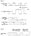
- FIG. 3 shows timing charts for explaining the overcurrent protection according to the first embodiment.
- the timing chart (a) in Figure 3 shows a typical wave form of an ON/OFF command (driver input) VinX, VinY, VinZ or VinDB inputted to the pre-driver 3X, 3Y, 3Z or 3DB from the main control board 05 of the inverter.
- the timing chart (b) in Figure 3 shows a typical wave form of a collector current of any of the IGBT's 1X through 1Z and 1DB flowing in response to the foregoing ON/OFF command when an overcurrent anomaly is caused.
- the timing chart (c) in Figure 3 shows the output timing of the preliminary alarm signal ALM2 outputted from the pertinent pre-driver 3X, 3Y, 3Z or 3DB based on the collector current (b) of Figure 3.
- the timing chart (d) in Figure 3 shows the output timing of the alarm signal ALM1.
- the wave forms (a) and (b) in Figure 3 are applied also to the inverter switches 1U through 1W on the upper arm.
- the pre-drivers 3U through 3W for the inverter switches on the upper arm also execute protecting operation at an alarm level Im1 of the collector current, although the pre-drivers 3U through 3W do not output the alarm signal ALM 1.
- the pre-driver, 3X, 3Y, 3Z or 3DB detects anomalous increase of the collector current of the corresponding IGBT that reaches the alarm level Im1 at a time t1
- the pertinent pre-driver, 3X, 3Y, 3Z or 3DB stops the operation of the corresponding IGBT, in the same manner as the conventional inverter does, and sets the signal on the alarm enable line 5 at a low level Lo to output an alarm signal ALM1.
- the pertinent pre-driver, 3X, 3Y, 3Z or 3DB sets the signal on the preliminary alarm line 6 at a low level Lo to output a preliminary alarm signal ALM2 to the main control board 05 of the inverter.
- the corresponding IGBT is not turned off.
- the low signal level Lo on the preliminary alarm line 6 does not affect the other pre-drivers connected to the preliminary alarm line 6.
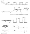
- FIG. 2 shows timing charts for explaining the overheat protection according to the second embodiment of the invention.
- the timing chart (a) in Figure 2 shows a typical wave form of a driver input VinX, VinY, VinZ or VinDB inputted to the pre-driver 3X, 3Y, 3Z or 3DB from the main control board 05 of the inverter.
- the timing chart (c) in Figure 2 shows a typical wave form of a collector current of any of the IGBT's 1X through 1Z and 1DB flowing in response to the foregoing driver input.
- the timing chart (b) in Figure 2 shows a typical temperature change, including anomalous heat up of the IGBT chip, caused by the collector current of (c) in Figure 2.
- the timing chart (d) in Figure 2 shows the output timing of the preliminary alarm signal ALM2 outputted from the pertinent pre-driver 3X, 3Y, 3Z or 3DB based on the chip temperature detection in (b) of Figure 2.
- the timing chart (e) in Figure 2 shows the output timing of the alarm signal ALM1.
- the wave forms (a) and (c) in Figure 2 are applied also to the inverter switches 1U through 1W on the upper arm.
- the pre-drivers 3U through 3W for the inverter switches on the upper arm also execute protecting operation at an alarm level ⁇ m1 for the temperature of the corresponding IGBT chip, although the pre-drivers 3U through 3W do not output the alarm signal ALM 1.
- the pre-driver, 3X, 3Y, 3Z or 3DB detects anomalous heat up of the corresponding IGBT chip that reaches the alarm level ⁇ m1 (from 160 to 170°) at a time t1
- the pertinent pre-driver, 3X, 3Y, 3Z or 3DB stops the operation of the corresponding IGBT, in the same manner as the conventional inverter does, and sets the signal on the alarm enable line 5 at a low level Lo to output an alarm signal ALM1.
- the chip temperature exceeding the normal value reaches the preliminary alarm level ⁇ m2 (e.g.
- the pertinent pre-driver, 3X, 3Y, 3Z or 3DB sets the signal on the preliminary alarm line 6 at a low level Lo to output a preliminary alarm signal ALM2 to the main control board 05 of the inverter.
- the corresponding IGBT will not be turned off.
- the low signal level Lo on the preliminary alarm line 6 does not affect the other pre-drivers connected to the preliminary alarm line 6.
- the alarm enable line 5 for outputting the alarm signal ALM1 and the preliminary alarm line 6 for outputting the preliminary alarm signal ALM2 are used.
- one alarm signal line may be used commonly for outputting the alarm signal ALM1 and for outputting the preliminary alarm signal ALM2. (That is, the conventional output terminals used for outputting the alarm signal ALM1 may be used also for outputting the preliminary alarm signal ALM2.)
- Figure 4 shows the wave forms of the alarm signals and the preliminary alarm signal on a common alarm signal line (i.e. on the common output terminal for outputting the alarm signals).
- the output width T2 for which the signal is set at the low level Lo, for the preliminary alarm signal ALM2 and the output width T1, for which the signal is set at the low level Lo, for the alarm signal ALM1 are different so that these alarm signals ALM1 and ALM2 are distinguishable form each other.
- the other pro-drivers As soon as the other pre-drivers, which did not output the alarm signal ALM1, detect the low signal level Lo on the alarm enable line 5, the other pro-drivers turn off the corresponding IGBT's.
- the pro-driver 3DB for the breaking switch does not turn off the corresponding IGBT 1DB even when the signal on the alarm enable line 5 is set at the low level Lo.
- the pro-driver 3DB for the braking IGBT 1DB does not turn off the IGBT 1DB so that the IGBT 1DB may keep executing the switching operation (as far as the pro-driver 3DB has not outputted the alarm signal ALM1).
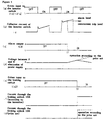
- Figure 5 shows timing charts for explaining the operation of the braking IGBT 1DB according to the fourth embodiment of the invention.
- the timing chart (a) in Figure 5 shows a typical wave form of an ON/OFF command (driver input) VinX, VinY or VinZ inputted to the pro-driver 3X, 3Y or 3Z from the main control board 05 of the inverter.
- the timing chart (b) in Figure 5 shows a typical wave form of a collector current of any of the IGBT's 1X through 1Z flowing in response to the foregoing ON/OFF command when an overcurrent anomaly is caused.
- the timing chart (c) in Figure 5 shows the output timing of the alarm signal ALM1 outputted from the pertinent pre-driver 3X, 3Y or 3Z based on the collector overcurrent (b) of Figure 5.
- the timing chart (d) in Figure 5 shows the change of the voltage between the electrodes P and N of the main DC power supply 02 with elapse of time.
- the timing chart (e) in Figure 5 shows the output timing of the ON/OFF command (driver input) VinDB from the main control board 05 of the inverter, that monitors the voltage (d) in Figure 5 across the main DC power supply 02, to the pre-driver 3DB for the braking IGBT 1DB.
- the timing chart (f) in Figure 5 shows the timing, thereat a current flows through the braking IGBT 1DB switched on and off based on the driver input VinDB of (e) in Figure 5.
- the pertinent pre-driver, 3X, 3Y or 3Z stops the operation of the corresponding IGBT, in the same manner as the conventional inverter does, and sets the signal on the alarm enable line 5 at a low level Lo to output an alarm signal ALM1.
- the other pre-drivers which have detected the low signal level Lo on the alarm enable line 5, turn off the corresponding IGBT's on the lower arm.
- All the IGBT's on the upper arm of the inverter are also turned off in response to the OFF command outputted from the main control board 05 of the inverter that has detected the alarm signal ALM1. As all the IGBT's on the upper and lower arms are turned off, the voltage between the P and N electrodes of the main DC power supply 02 is raised by the energy regenerated from the motor 03.
- the main control board 05 of the inverter detects that the voltage between the P and N electrodes of the main DC power supply 02 exceeding a predetermined value at a time t3
- the main control board 05 of the inverter outputs the driver input VinDB, that is an ON command (strictly describing an ON/OFF signal with a short period) to the pre-driver 3DB for the braking IGBT 1DB to intermittently switch on the braking IGBT 1DB.
- the intelligent power module that is a semiconductor apparatus incorporating semiconductor switching devices, pre-drivers and control circuits in a package, outputs a preliminary alarm signal ALM2, without stopping the power conversion, as soon as a sign of an anomaly in any of the inverter switches is detected, in advance to turning off the inverter switches to remove the anomaly caused in any of the inverter switches.
- the sign of an anomaly in any of the inverter switches is detected at a time when the collector current or the chip temperature of any of the inverter switches exceeds a predetermined value higher than the normal value but lower than the anomalous value.
- the IMP according to the first aspect of the invention facilitates removing the causes which may cause a real anomaly in advance and avoiding anomalous sudden stop of the inverter that may affect the factory operation very badly.
- any of the protection circuits turns off corresponding one of the inverter switches and the braking switch and outputs an alarm signal via a common signal line when an anomaly is caused in the corresponding one of the inverter switches and the braking switch.
- the other pre-drives of the inverter switches which have received the alarm signal via the common signal line, turn off the corresponding inverter switches, but the pre-driver for the braking switch does not turn off the braking switch even when an alarm signal is outputted from any of the pre-drivers for the inverter switches.
- the power supply voltage is prevented from further rising by consuming the regenerated energy by intermittently switching on the braking switch.
- the over voltage exceeding the breakdown voltages of the semiconductor devices and such constituent elements of the IMP may not be applied thereto.
Landscapes
- Engineering & Computer Science (AREA)
- Power Engineering (AREA)
- Inverter Devices (AREA)
- Control Of Ac Motors In General (AREA)
- Power Conversion In General (AREA)
Abstract
Description
- The present invention relates to a semiconductor apparatus incorporated in a power converting apparatus such as an inverter for variably controlling the speed of a motor. More specifically, the present invention relates to a so-called intelligent power module (hereinafter referred to as an "IPM") that incorporates semiconductor switching devices for power conversion, driver circuits for driving the respective semiconductor switching devices and various protection circuits in a package.
- Figure 6 is a block diagram showing the main portion of a conventional inverter for variably controlling the speed of a motor including an intelligent power module (IPM). In the figure, there are shown an
IPM 01, a mainDC power supply 02 formed of a not shown rectifier circuit in amain control board 05 of the inverter, amotor 03, the speed thereof is variably controlled by the inverter, and aresistor 04 in themain control board 05 of the inverter for consuming regenerated electric power. Theresistor 04 will be described later in detail. - The
main control board 05 of the inverter includes the above described rectifier circuit that constitutes the mainDC power supply 02, the control circuits which generate various control signals for controlling theIPM 01, and such control circuits. - The IPM01 includes semiconductor switching devices which also work as sensing IGBT's 1 (1U through 1Z and 1DB), each having a sensing terminal SE for dividing the emitter current thereof and for detecting anomalies in the emitter current caused by short circuit in the load and such causes. In the following, the IGBT's 1U through 1Z will be sometimes referred to as the "inverter switches" and the IGBT 1DB as the "braking switch".
- The IPM01 includes free wheel diodes 2 (2U through 2Z and 2DB). Each of the free wheel diodes 2U through 2Z is connected in opposite parallel between the collector and the emitter of each of the IGBT's (inverter switches) 1U through 1Z. The free wheel diode 2DB is connected in parallel to the
resistor 04 in such a polarity that the cathode of the diode 2DB is connected to the positive electrode P of the mainDC power supply 02. - The IPM01 includes pre-drivers 3 (3U through 3Z and 3DB) disposed in one to one correspondence to the IGBT's 1 (1U through 1Z and 1DB). In Figure 6, one pre-driver is used to drive one IGBT. Alternatively, one pre-driver may be used to drive all the inverter switches 1U through 1Z, two pre-drivers may be used to drive the inverter switches on the upper arm and the inverter switches on the lower arm respectively, or one pre-driver may be used to drive all the inverter switches 1U through 1Z and the braking switch 1DB.
- The IGBT's 1U and 1X are connected in series to each other and in forward between the positive electrode P and the negative electrode N of the main
DC power supply 02 such that the IGBT 1U is on the upper arm and theIGBT 1X is on the lower arm of the inverter bridge. The IGBT's 1V and 1Y are connected in series to each other and in forward between the positive electrode P and the negative electrode N of the mainDC power supply 02 such that theIGBT 1V is on the upper arm and theIGBT 1Y is on the lower arm. And, the IGBT's 1W and 1Z are connected in series to each other and in forward between the positive electrode P and the negative electrode N of the mainDC power supply 02 such that theIGBT 1W is on the upper arm and the IGBT 1Z is on the lower arm. - Six inverter switches, i.e. the IGBT's 1U through 1Z, constitute a three-phase inverter bridge circuit. The mutual connection point of the IGBT's 1U and 1X is connected to an output terminal U for the U phase of a three-phase alternating current. The mutual connection point of the IGBT's 1V and 1Y is connected to an output terminal V for the V phase of the three-phase alternating current. And, the mutual connection point of the IGBT's 1W and 1Z is connected to an output terminal W for the W phase of the three-phase alternating current. The output terminals U, V and W are connected to the motor (a three-phase induction motor in Figure 6) 03. The braking switch, i.e. the IGBT 1DB, is connected in series to the
resistor 04 for consuming the regenerated electric power and in forward between the P and N electrodes of the mainDC power supply 02. - Each of the pre-drivers 3U through 3Z and 3DB includes a circuit for driving the gate of the corresponding IGBT and protection circuits. A driving power supply (DC 15 V in Figure 6) is fed to the pre-drivers 3U through 3Z and 3DB. Fundamentally, the pre-drivers 3U through 3Z and 3DB work as driver circuits which feed a gate signal, indicative of ON or OFF of the corresponding IGBT, between the gate and the emitter thereof, when an ON-signal or an OFF signal (hereinafter referred to as a "driver input") is inputted from the
main control board 05 of the inverter to any of the terminals VinU through VinZ and VinDB, to switch on or off the corresponding IGBT. - Usually, a three-phase AC voltage, the voltage and the frequency thereof are variable, is generated through the IGBT's 1U through IZ which convert the electric power from the main
DC power supply 02 to control the speed of themotor 03 variably. - When the output frequency of the inverter is decreased to decelerate or stop the
motor 03 while themotor 03 is driven, the energy of themotor 03 is regenerated to the mainDC power supply 02, and the voltage between the electrodes P and N of theDC power supply 02 rises. As the voltage rises to much, an over voltage exceeding the breakdown voltages of the IGBT's and the smoothing capacitor in theDC power supply 02 may be applied thereto. - To avoid this, the
main control board 05 of the inverter monitors the voltage between the electrodes P and N of theDC power supply 02. When the voltage between the electrodes P and N of theDC power supply 02 exceeds a predetermined value, the control circuit feeds ON and OFF signals to the input terminal VinDB of the pre-driver 3DB for the braking switch, i.e. the IGBT 1DB to intermittently switch on the IGBT 1DB. As the IGBT 1DB is switched on intermittently, the electric power regenerated from themotor 03 to theDC power supply 02 is bypassed to theresistor 04, therein the regenerated electric power is consumed. Thus, the voltage between the electrodes of the mainDC power supply 02 is prevented from increasing too much. - The pre-drivers 3 described above exhibit the function of 1) driving of the IGBT's and various protection functions, such as 2) protection against short circuit, 3) protection against a low voltage, 4) protection against an overcurrent, and 5) protection against overheat of the IGBT's.
- In the protection against short circuit 2), the pre-drivers 3 monitor the output currents from the sensing terminals SE of the IGBT's at a high speed. When any of the monitored output currents exceeds a predetermined level (set, for example, at a value from 4 to 5 times as large as the rated current), the pertinent pre-driver 3 turns off the corresponding IGBT in a very short time (by the so-called soft interruption that lowers the gate voltage at first and, then, turns off the IGBT) so that the pertinent IGBT may be protected.
- The protection against a low voltage 3) is conducted to keep the gate voltages of the IGBT's at an optimum value. In the protection against a low voltage 3), the pre-drivers 3 monitor the driving voltages, which the pre-drivers 3 feed to the IGBT's. When any of the monitored driving voltages is lower than a predetermined value, the pertinent pre-driver 3 turns off the corresponding IGBT so that the IGBT may be protected.
- In the overcurrent protection 4), the pre-drivers 3 monitors the output currents from the sensing terminals SE of the IGBT's. When any of the monitored output currents exceeds a predetermined level (set, for example, at a value from 1.5 times to twice as large as the rated current), the pertinent pre-drivers 3 turns off the corresponding IGBT. The detection speed and the detection level for the overcurrent protection 4) are different from those for the short circuit protection 2).
- In the overheat protection 5), the pre-drivers 3 monitor the temperatures of the chips, in which the respective IGBT's are buried, by detecting the forward currents of the diodes buried in the chips. When any of the monitored temperatures exceeds a predetermined temperature, the pertinent pre-driver 3 turns off the corresponding IGBT.
- There is shown an overheat protection circuit 4 in the bottom of Figure 6. Usually, the signal on an alarm enable
line 5 is set at a high level Hi. When any of the temperatures of metallic or ceramic insulation substrates, which insulate the chips of the IGBT's 1U through 1Z and 1DB from the respective metallic radiator substrates, exceeds a predetermined temperature, the overheat protection circuit 4 sets the signal on the alarm enableline 5, usually at a high level Hi, at a low level Lo to output an alarm signal ALM at the low level Lo. - When any of the pre-drivers 3X through 3Z, which drive the IGBT's 1X through 1Z constituting the lower arm of the inverter bridge circuit, executes any of the protection operations 2) through 4) the pertinent pre-driver 3X, 3Y or 3Z sets the signal on the alarm enable
line 5 at the low level Lo to output an alarm signal ALM at the low level Lo, similarly as the overheat protection circuit 4 does. - When the alarm signal ALM is outputted, i.e. when alarm enable
line 5 is active, the pre-drivers which have not outputted the alarm signal ALM detect the alarm signal ALM at the low level Lo and turn off the respective IGBT's. - When the
main control board 05 of the inverter detects the alarm signal ALM at the low level Lo, themain control board 05 of the inverter outputs an OFF-signal to the pre-drivers 3U through 3W which drive the IGBT's 1U through 1W on the upper arm of the inverter bridge circuit to turn off the IGBT's 1U through 1W. - Thus, when any of the pre-drivers 3U through 3Z and 3DB and the overheat protection circuit 4 executes any of the protection operations, all the IGBT's 1U through 1Z and 1DB are turned off.
- As described above, the conventional IPM exhibits the protection functions mainly to protect the semiconductor devices which the IPM incorporates against anomalies and to avoid breakdown of the semiconductor devices. As soon as the IPM detects an anomaly, all the IGBT's are turned off to stop the operations of the inverter.
- Therefore, if an anomaly is caused in the inverter, breakdown of the semiconductor devices will be avoided. However, when an inverter, operated in a manufacturing line in an unnoticeable overloaded state, suddenly stops, the operation of an entire factory system slows down or stops.
- Especially in a large manufacturing line, tremendous loses are caused. Therefore, it is desired to avoid slowdown or stop of the operation of the factory system by detecting a sign indicating possible anomalous stop of the inverter, by outputting a preliminary alarm signal and by guiding the operators of the inverter to remove the causes which may cause anomalous stop of the inverter in advance to real anomalous stop of the inverter.
- As described above, as soon as any of the pre-drivers 3X through 3Z for the inverter switches detects an anomaly, the signal on the alarm enable
line 5 is set at the low level Lo, thereby the operation of the braking switch, i.e. IGBT 1DB, is also stopped. - When the operation of the inverter circuit is stopped suddenly by an anomaly caused in the inverter switches, the energy of the rotating
motor 03, i.e. a load, is regenerated back to the mainDC power supply 02, and the voltage across the mainDC power supply 02 is raised. - As described above, when the
main control board 05 of the inverter detects the rise of the voltage across the mainDC power supply 02, the control circuit makes the braking IGBT 1DB work to suppress the rise of the voltage across the mainDC power supply 02 in usual. However, once the pre-driver 3DB, that detected the low signal level Lo on the alarm enableline 5, has turned off the braking IGBT 1DB, the braking IGBT 1DB never operates even when an ON-signal is fed to the input terminal VinBD of the pre-driver 3DB. Therefore, the voltage across the mainDC power supply 02 is not prevented from rising, and, in the worst case, breakdown of the constituent elements of the IPM is caused. - In view of the foregoing, it is an object of the invention to provide a semiconductor apparatus including an IMP that facilitates outputting a preliminary alarm signal without stopping the inverter when a sign of an anomaly in the IPM is detected, guiding removal of the causes which may cause anomalous stop of the inverter, and preventing the operation of the factory system from sudden slowdown or sudden stop. It is another object of the invention to provide a semiconductor apparatus including an IMP that facilitates intermittently switching on the braking IGBT and, thereby, preventing the voltage across the main DC power supply from rising even when any of the inverter switches is turned off due to an anomaly and the inverter is stopped.
- According to a first aspect of the invention, there is provided a semiconductor apparatus including one or more semiconductor switching devices for electric power conversion, one or more driver circuits disposed in one to one correspondence to the one or more semiconductor switching devices, the one or more driver circuits switching on and off corresponding one of the one or more semiconductor switching devices via the respective control terminals in response to an ON/OFF command inputted thereto from the outside, and one or more anomaly protection means disposed in one to one correspondence to the one or more semiconductor switching devices, the one or more anomaly protection means monitoring corresponding one of the one or more semiconductor switching devices, the one or more anomaly protection means ordering corresponding one of the one or more driver circuits to turn off the corresponding one of the one or more semiconductor switching devices when the one or more anomaly protection means have detected an anomaly in the corresponding one of the one or more semiconductor switching devices, the semiconductor apparatus further including: one or more anomaly predicting means disposed in one to one correspondence to the one or more semiconductor switching devices, the one or more anomaly predicting means outputting a preliminary alarm signal when the one or more anomaly predicting means have detected a sign of an anomaly in corresponding one of the one or more semiconductor switching devices.
- Advantageously, the one or more anomaly protection means judge that an anomaly is caused in corresponding one of the one or more semiconductor switching devices when the current flowing between the main terminals of the corresponding one of the one or more semiconductor switching devices has exceeded a first predetermined value higher than the normal value of the current, and the one or more anomaly predicting mean output the preliminary alarm signal when the current flowing between the main terminals of the corresponding one of the one or more semiconductor switching devices has exceeded a second predetermined value higher than the normal value of the current but lower than the first predetermined value.
- Advantageously, the one or more anomaly protection means judge that an anomaly is caused in corresponding one of the one or more semiconductor switching devices when the chip temperature of the corresponding one of the one or more semiconductor switching devices has exceeded a first predetermined temperature higher than the normal chip temperature, and the one or more anomaly predicting mean output the preliminary alarm signal when the chip temperature of the corresponding one of the one or more semiconductor switching devices has exceeded a second predetermined temperature higher than the normal chip temperature but lower than the first predetermined temperature.
- Advantageously, the one or more anomaly protection means output an alarm signal when the one or more anomaly protection means judge that the anomaly is caused in the corresponding one of the one or more semiconductor switching devices.
- Advantageously, the preliminary alarm signal and the alarm signal are digital signals, the pulse widths thereof are different from each other, and the digital signals are outputted from a common output terminal.
- According to a second aspect of the invention, there is provided a semiconductor apparatus including: an inverter for driving a motor, the inverter including a main circuit; the main circuit including one or more inverter semiconductor switches; a braking semiconductor switch, the braking semiconductor switch interrupting and making flow a current, thereby to consume energy regenerated from the motor; driver circuits disposed in one to one correspondence to the one or more inverter semiconductor switches and the braking semiconductor switch, the driver circuits switching on and off the corresponding one of the one or more inverter semiconductor switches and the braking semiconductor switch via the respective control terminals in response to an ON/OFF command inputted thereto from the outside; anomaly protection means disposed in one to one correspondence to the one or more inverter semiconductor switches and the braking semiconductor switch, the anomaly protection means monitoring corresponding one of the one or more inverter semiconductor switching devices and the braking semiconductor switching device, the anomaly protection means ordering corresponding one of the driver circuits to turn off the corresponding one of the one or more inverter semiconductor switches and the braking semiconductor switch when the anomaly protection means have detected an anomaly in the corresponding one of the one or more inverter semiconductor switches and the braking semiconductor switch; alarm signal outputting means disposed in one to one correspondence to the one or more inverter semiconductor switches and the braking semiconductor switch, each of the alarm signal outputting means outputting an alarm signal through a common signal line when an anomaly is caused in corresponding one of the one or more inverter semiconductor switches and the braking semiconductor switch; and one or more alarm signal receiving means disposed in one to one correspondence to the one or more inverter semiconductor switches, the one or more alarm signal receiving means order corresponding one of the anomaly protection means to turn off corresponding one of the one or more inverter semiconductor switches in response to the alarm signal inputted from the alarm signal outputting means of the other inverter semiconductor switch through the common signal line.
- Advantageously, the one or more alarm signal receiving means turn off the one or more inverter semiconductor switches.
- The characteristic functions of the semiconductor apparatus according to the invention are as follows.
- According to the first aspect of the invention, as soon as a sign of an anomaly in any of the inverter switches is detected, the IPM outputs a preliminary alarm signal ALM2, without stopping the electric power conversion, in advance to turning off the inverter switches to remove the cause of the anomaly.
- The sign of an anomaly in any of the inverter switches is detected at an instance when the collector current or the chip temperature of any of the inverter switches exceeds a predetermined value higher than the normal value but lower than the anomalous value.
- When a common terminal is used for outputting the alarm signal indicating an anomaly from the IPM and for outputting the preliminary alarm signal indicating a sign of an anomaly from the IPM, the pulse widths of the alarm signal and the preliminary alarm signal are set to be different from each other.
- The preliminary detection of a sign of an anomaly facilitates removing the causes which may cause a real anomaly and avoiding anomalous sudden stop of the inverter in advance.
- According to the second aspect of the invention, when an anomaly is caused in any of the inverter switches and the braking switch, the corresponding pre-driver turns off the pertinent switch and outputs an alarm signal via a common signal line. The other pre-drives of the inverter switches, which have received the alarm signal via the common signal line, turn off the corresponding inverter switches.
- The pre-driver for the braking switch does not turn off the braking switch even when an alarm signal is outputted from any of the pre-drivers for the inverter switches.
- Even when the inverter stops suddenly and the power supply voltage rises due to the regenerated energy from the motor, the power supply voltage is prevented from further rising by consuming the regenerated energy by the ON/OFF operation of the braking switch.
- Now the invention will be explained hereinafter with reference to the accompanying drawings which illustrate the preferred embodiment of the invention. Throughout the following drawing figures, the same reference numerals as used in Figure 6 are used to designate the same or corresponding constituent elements.
- Figure 1 is a block diagram showing the main portion of an inverter for variably controlling the speed of a motor according to the first embodiment of the invention including an intelligent power module (IPM) 01;
- Figure 2 shows timing charts for explaining the overheat protection according to the second embodiment of the invention;
- Figure 3 shows timing charts for explaining the overcurrent protection according to the first embodiment of the invention;
- Figure 4 shows the wave forms of the alarm signal and the preliminary alarm signal on the common alarm signal line according to the third embodiment of the invention;
- Figure 5 shows timing charts for explaining the operations of the braking IGBT according to the fourth embodiment of the invention; and
- Figure 6 is a block diagram showing the main portion of a conventional inverter for variably controlling the speed of a motor including an intelligent power module (IPM).
-
- Referring now to Figure 1, the
IPM 01 includes pre-drivers 3X through 3Z and 3DB which output analarm signal ALM 1 to amain control board 05 of the inverter via an alarm enableline 5. The inverter according to the first embodiment is different from the conventional inverter in that the inverter according to the first embodiment includes apreliminary alarm line 6, through which the pre-drivers 3X through 3Z and 3DB output a preliminaryalarm signal ALM 2, and in that the pre-drivers 3U through 3W for the inverter switches on the upper arm also output respective alarm signals ALM1U through ALM1W and respective preliminary alarm signals ALM2U through ALM2W. - By making the pre-drivers 3U through 3W output respective alarm signals ALM1U through ALM1W and respective preliminary alarm signals ALM2U through ALM2W, more precise control may be executed. The functions of the pre-drivers same with the conventional pre-divers may be assigned to one or less number of pre-drivers.
- Figure 3 shows timing charts for explaining the overcurrent protection according to the first embodiment. The timing chart (a) in Figure 3 shows a typical wave form of an ON/OFF command (driver input) VinX, VinY, VinZ or VinDB inputted to the pre-driver 3X, 3Y, 3Z or 3DB from the
main control board 05 of the inverter. The timing chart (b) in Figure 3 shows a typical wave form of a collector current of any of the IGBT's 1X through 1Z and 1DB flowing in response to the foregoing ON/OFF command when an overcurrent anomaly is caused. - The timing chart (c) in Figure 3 shows the output timing of the preliminary alarm signal ALM2 outputted from the
pertinent pre-driver - Even when the upper arm of the inverter is not provided with the alarm output function, the wave forms (a) and (b) in Figure 3 are applied also to the inverter switches 1U through 1W on the upper arm. The pre-drivers 3U through 3W for the inverter switches on the upper arm also execute protecting operation at an alarm level Im1 of the collector current, although the pre-drivers 3U through 3W do not output the
alarm signal ALM 1. - As shown in Figure 3, when the pre-driver, 3X, 3Y, 3Z or 3DB detects anomalous increase of the collector current of the corresponding IGBT that reaches the alarm level Im1 at a time t1, the pertinent pre-driver, 3X, 3Y, 3Z or 3DB stops the operation of the corresponding IGBT, in the same manner as the conventional inverter does, and sets the signal on the alarm enable
line 5 at a low level Lo to output an alarm signal ALM1. In advance, as soon as the collector current exceeding the normal value reaches a preliminary alarm level Im2 at a time t2, the pertinent pre-driver, 3X, 3Y, 3Z or 3DB sets the signal on thepreliminary alarm line 6 at a low level Lo to output a preliminary alarm signal ALM2 to themain control board 05 of the inverter. - As far as only the preliminary alarm signal ALM2 is outputted, the corresponding IGBT is not turned off. The low signal level Lo on the
preliminary alarm line 6 does not affect the other pre-drivers connected to thepreliminary alarm line 6. - Figure 2 shows timing charts for explaining the overheat protection according to the second embodiment of the invention. The timing chart (a) in Figure 2 shows a typical wave form of a driver input VinX, VinY, VinZ or VinDB inputted to the pre-driver 3X, 3Y, 3Z or 3DB from the
main control board 05 of the inverter. The timing chart (c) in Figure 2 shows a typical wave form of a collector current of any of the IGBT's 1X through 1Z and 1DB flowing in response to the foregoing driver input. The timing chart (b) in Figure 2 shows a typical temperature change, including anomalous heat up of the IGBT chip, caused by the collector current of (c) in Figure 2. - The timing chart (d) in Figure 2 shows the output timing of the preliminary alarm signal ALM2 outputted from the
pertinent pre-driver - The wave forms (a) and (c) in Figure 2 are applied also to the inverter switches 1U through 1W on the upper arm. The pre-drivers 3U through 3W for the inverter switches on the upper arm also execute protecting operation at an alarm level m1 for the temperature of the corresponding IGBT chip, although the pre-drivers 3U through 3W do not output the
alarm signal ALM 1. - As shown in Figure 2, when the pre-driver, 3X, 3Y, 3Z or 3DB detects anomalous heat up of the corresponding IGBT chip that reaches the alarm level m1 (from 160 to 170°) at a time t1, the pertinent pre-driver, 3X, 3Y, 3Z or 3DB stops the operation of the corresponding IGBT, in the same manner as the conventional inverter does, and sets the signal on the alarm enable
line 5 at a low level Lo to output an alarm signal ALM1. In advance, as soon as the chip temperature exceeding the normal value reaches the preliminary alarm level m2 (e.g. 130°) at a time t2, the pertinent pre-driver, 3X, 3Y, 3Z or 3DB sets the signal on thepreliminary alarm line 6 at a low level Lo to output a preliminary alarm signal ALM2 to themain control board 05 of the inverter. - As far as only the preliminary alarm signal ALM2 is outputted, the corresponding IGBT will not be turned off. The low signal level Lo on the
preliminary alarm line 6 does not affect the other pre-drivers connected to thepreliminary alarm line 6. - In the first and second embodiments, the alarm enable
line 5 for outputting the alarm signal ALM1 and thepreliminary alarm line 6 for outputting the preliminary alarm signal ALM2 are used. Alternatively, one alarm signal line may be used commonly for outputting the alarm signal ALM1 and for outputting the preliminary alarm signal ALM2. (That is, the conventional output terminals used for outputting the alarm signal ALM1 may be used also for outputting the preliminary alarm signal ALM2.) - Figure 4 shows the wave forms of the alarm signals and the preliminary alarm signal on a common alarm signal line (i.e. on the common output terminal for outputting the alarm signals). As shown in Figure 4, the output width T2, for which the signal is set at the low level Lo, for the preliminary alarm signal ALM2 and the output width T1, for which the signal is set at the low level Lo, for the alarm signal ALM1 are different so that these alarm signals ALM1 and ALM2 are distinguishable form each other.
- In Figure 3 or 2, when the collector current or the chip temperature, that has been increasing after the preliminary alarm signal ALM2 was outputted, reaches the alarm level Im1 or m1 for outputting the alarm signal ALM1, the
pertinent pre-driver line 5 at the low level Lo and outputs the alarm signal ALM1 at the low signal level Lo to themain control board 05 of the inverter. - As soon as the other pre-drivers, which did not output the alarm signal ALM1, detect the low signal level Lo on the alarm enable
line 5, the other pro-drivers turn off the corresponding IGBT's. - In contrast, according to the fourth embodiment of the invention, the pro-driver 3DB for the breaking switch does not turn off the corresponding IGBT 1DB even when the signal on the alarm enable
line 5 is set at the low level Lo. - According to the fourth embodiment of the invention, even when the signal on the alarm enable
line 5 is set at the low level Lo in association with the protecting operation and the output of the alarm signal ALM1 by any of the pro-drivers 3X through 3Z connected to the alarm enableline 5, the pro-driver 3DB for the braking IGBT 1DB does not turn off the IGBT 1DB so that the IGBT 1DB may keep executing the switching operation (as far as the pro-driver 3DB has not outputted the alarm signal ALM1). - Figure 5 shows timing charts for explaining the operation of the braking IGBT 1DB according to the fourth embodiment of the invention.
- The timing chart (a) in Figure 5 shows a typical wave form of an ON/OFF command (driver input) VinX, VinY or VinZ inputted to the pro-driver 3X, 3Y or 3Z from the
main control board 05 of the inverter. The timing chart (b) in Figure 5 shows a typical wave form of a collector current of any of the IGBT's 1X through 1Z flowing in response to the foregoing ON/OFF command when an overcurrent anomaly is caused. - The timing chart (c) in Figure 5 shows the output timing of the alarm signal ALM1 outputted from the
pertinent pre-driver DC power supply 02 with elapse of time. - The timing chart (e) in Figure 5 shows the output timing of the ON/OFF command (driver input) VinDB from the
main control board 05 of the inverter, that monitors the voltage (d) in Figure 5 across the mainDC power supply 02, to the pre-driver 3DB for the braking IGBT 1DB. The timing chart (f) in Figure 5 shows the timing, thereat a current flows through the braking IGBT 1DB switched on and off based on the driver input VinDB of (e) in Figure 5. - Note that (e) and (f) in Figure 5 show macroscopic transitions with elapse of time. In practice, the ON signal at the low level Lo of the driver input VinDB is an ON/OFF signal with a short period. The current (f) in Figure 5 through the braking switch 1DB has a wave form corresponding to the driver input VinDB shown by (e) in Figure 5.
- As soon as the pre-driver, 3X, 3Y or 3Z detects anomalous increase of the collector current of the corresponding IGBT that reaches the alarm level Im1 at a time t1, the pertinent pre-driver, 3X, 3Y or 3Z stops the operation of the corresponding IGBT, in the same manner as the conventional inverter does, and sets the signal on the alarm enable
line 5 at a low level Lo to output an alarm signal ALM1. At the same time, the other pre-drivers, which have detected the low signal level Lo on the alarm enableline 5, turn off the corresponding IGBT's on the lower arm. - All the IGBT's on the upper arm of the inverter are also turned off in response to the OFF command outputted from the
main control board 05 of the inverter that has detected the alarm signal ALM1. As all the IGBT's on the upper and lower arms are turned off, the voltage between the P and N electrodes of the mainDC power supply 02 is raised by the energy regenerated from themotor 03. - As soon as the
main control board 05 of the inverter detects that the voltage between the P and N electrodes of the mainDC power supply 02 exceeding a predetermined value at a time t3, themain control board 05 of the inverter outputs the driver input VinDB, that is an ON command (strictly describing an ON/OFF signal with a short period) to the pre-driver 3DB for the braking IGBT 1DB to intermittently switch on the braking IGBT 1DB. By intermittently switching on the braking IGBT 1DB, the energy regenerated from the motor is consumed by theresistor 04 so that the voltage across the mainDC power supply 02 may be prevented from rising and an over voltage exceeding the breakdown voltages of the semiconductor devices and such constituent elements of the IMP may not be applied thereto. - According to the first aspect of the invention, the intelligent power module (IPM), that is a semiconductor apparatus incorporating semiconductor switching devices, pre-drivers and control circuits in a package, outputs a preliminary alarm signal ALM2, without stopping the power conversion, as soon as a sign of an anomaly in any of the inverter switches is detected, in advance to turning off the inverter switches to remove the anomaly caused in any of the inverter switches. The sign of an anomaly in any of the inverter switches is detected at a time when the collector current or the chip temperature of any of the inverter switches exceeds a predetermined value higher than the normal value but lower than the anomalous value. The IMP according to the first aspect of the invention facilitates removing the causes which may cause a real anomaly in advance and avoiding anomalous sudden stop of the inverter that may affect the factory operation very badly.
- In the IMP according to the second aspect of the invention that incorporates semiconductor switching devices constituting the bridge circuit for power conversion (inverter switches), a semiconductor switching device for interrupting and making flow a current for consuming the regenerated energy from a motor (braking switch), pre-drivers and control circuits thereof in a package, any of the protection circuits turns off corresponding one of the inverter switches and the braking switch and outputs an alarm signal via a common signal line when an anomaly is caused in the corresponding one of the inverter switches and the braking switch. The other pre-drives of the inverter switches, which have received the alarm signal via the common signal line, turn off the corresponding inverter switches, but the pre-driver for the braking switch does not turn off the braking switch even when an alarm signal is outputted from any of the pre-drivers for the inverter switches.
- Therefore, even when the inverter stops suddenly and the power supply voltage rises due to the regenerated energy from the motor, the power supply voltage is prevented from further rising by consuming the regenerated energy by intermittently switching on the braking switch. Thus, the over voltage exceeding the breakdown voltages of the semiconductor devices and such constituent elements of the IMP may not be applied thereto.
Claims (7)
- A semiconductor apparatus includingone or more semiconductor switching devices for electric power conversion,one or more driver circuits disposed in one to one correspondence to said one or more semiconductor switching devices, said one or more driver circuits switching on and off corresponding one of said one or more semiconductor switching devices via the respective control terminals in response to an ON/OFF command inputted thereto from the outside, andone or more anomaly protection means disposed in one to one correspondence to said one or more semiconductor switching devices, said one or more anomaly protection means monitoring corresponding one of said one or more semiconductor switching devices, said one or more anomaly protection means ordering corresponding one of said one or more driver circuits to turn off said corresponding one of said one or more semiconductor switching devices when said one or more anomaly protection means have detected an anomaly in said corresponding one of said one or more semiconductor switching devices,said semiconductor apparatus comprising:one or more anomaly predicting means disposed in one to one correspondence to said one or more semiconductor switching devices, said one or more anomaly predicting means outputting a preliminary alarm signal when said one or more anomaly predicting means have detected a sign of an anomaly in corresponding one of said one or more semiconductor switching devices.
- The semiconductor apparatus according to Claim 1, wherein said one or more anomaly protection means judge that an anomaly is caused in corresponding one of said one or more semiconductor switching devices when the current flowing between the main terminals of said corresponding one of said one or more semiconductor switching devices has exceeded a first predetermined value higher than the normal value of said current, and said one or more anomaly predicting mean output said preliminary alarm signal when said current flowing between said main terminals of said corresponding one of said one or more semiconductor switching devices has exceeded a second predetermined value higher than said normal value of said current but lower than said first predetermined value.
- The semiconductor apparatus according to Claim 1 or 2, wherein said one or more anomaly protection means judge that an anomaly is caused in corresponding one of said one or more semiconductor switching devices when the chip temperature of said corresponding one of said one or more semiconductor switching devices has exceeded a first predetermined temperature higher than the normal chip temperature, and said one or more anomaly predicting mean output said preliminary alarm signal when said chip temperature of said corresponding one of said one or more semiconductor switching devices has exceeded a second predetermined temperature higher than said normal chip temperature but lower than said first predetermined temperature.
- The semiconductor apparatus according to any of Claims 1 through 3, wherein said one or more anomaly protection means output an alarm signal when said one or more anomaly protection means judge that said anomaly is caused in said corresponding one of said one or more semiconductor switching devices.
- The semiconductor apparatus according to Claim 4, wherein said preliminary alarm signal and said alarm signal are digital signals, the pulse widths thereof are different from each other, and said digital signals are outputted from a common output terminal.
- A semiconductor apparatus comprising:an inverter for driving a motor, said inverter including a main circuit;said main circuit comprising one or more inverter semiconductor switches;a braking semiconductor switch, said braking semiconductor switch interrupting and making flow a current, thereby to consume energy regenerated from said motor;driver circuits disposed in one to one correspondence to said one or more inverter semiconductor switches and said braking semiconductor switch, said driver circuits switching on and off said corresponding one of said one or more inverter semiconductor switches and said braking semiconductor switch via the respective control terminals in response to an ON/OFF command inputted thereto from the outside;anomaly protection means disposed in one to one correspondence to said one or more inverter semiconductor switches and said braking semiconductor switch, said anomaly protection means monitoring corresponding one of said one or more inverter semiconductor switches and said braking semiconductor switch, said anomaly protection means ordering corresponding one of said driver circuits to turn off said corresponding one of said one or more inverter semiconductor switches and said braking semiconductor switch when said anomaly protection means have detected an anomaly in said corresponding one of said one or more inverter semiconductor switches and said braking semiconductor switch;alarm signal outputting means disposed in one to one correspondence to said one or more inverter semiconductor switches and said braking semiconductor switch, each of said alarm signal outputting means outputting an alarm signal through a common signal line when an anomaly is caused in corresponding one of said one or more inverter semiconductor switches and said braking semiconductor switch; andone or more alarm signal receiving means disposed in one to one correspondence to said one or more inverter semiconductor switches, said one or more alarm signal receiving means order corresponding one of said anomaly protection means to turn off corresponding one of said one or more inverter semiconductor switches in response to said alarm signal inputted from said alarm signal outputting means of the other inverter semiconductor switch through said common signal line.
- The semiconductor apparatus according to Claim 6, wherein said one or more alarm signal receiving means turn off said one or more inverter semiconductor switches.
Applications Claiming Priority (2)
| Application Number | Priority Date | Filing Date | Title |
|---|---|---|---|
| JP14755099 | 1999-05-27 | ||
| JP14755099A JP3635988B2 (en) | 1999-05-27 | 1999-05-27 | Semiconductor device |
Publications (3)
| Publication Number | Publication Date |
|---|---|
| EP1056205A2 true EP1056205A2 (en) | 2000-11-29 |
| EP1056205A3 EP1056205A3 (en) | 2005-01-19 |
| EP1056205B1 EP1056205B1 (en) | 2012-07-04 |
Family
ID=15432871
Family Applications (1)
| Application Number | Title | Priority Date | Filing Date |
|---|---|---|---|
| EP00304324A Expired - Lifetime EP1056205B1 (en) | 1999-05-27 | 2000-05-23 | Semiconductor apparatus |
Country Status (3)
| Country | Link |
|---|---|
| US (1) | US6459380B1 (en) |
| EP (1) | EP1056205B1 (en) |
| JP (1) | JP3635988B2 (en) |
Cited By (7)
| Publication number | Priority date | Publication date | Assignee | Title |
|---|---|---|---|---|
| FR2821213A1 (en) * | 2001-02-19 | 2002-08-23 | Mitsubishi Electric Corp | SEMICONDUCTOR DEVICE HAVING PROTECTIVE FUNCTION |
| WO2004068710A3 (en) * | 2003-01-24 | 2004-12-09 | Siemens Ag | Circuit arrangement for protecting a final power output element comprising semiconductor switches |
| EP1914873A4 (en) * | 2005-07-12 | 2009-05-13 | Daikin Ind Ltd | POLYPHASE INVERTER, METHOD OF CONTROLLING THE SAME, FAN AND POLYPHASE CURRENT SUPPLY SYSTEM |
| WO2012118701A3 (en) * | 2011-02-28 | 2013-03-21 | General Electric Company | System and method for operating inverters |
| US10374593B2 (en) | 2014-09-29 | 2019-08-06 | Fuji Electric Co., Ltd. | Semiconductor device |
| CN113325898A (en) * | 2021-05-31 | 2021-08-31 | 深圳市白光电子科技有限公司 | Starting protection circuit of thermosensitive temperature controller |
| US11515869B2 (en) | 2020-06-04 | 2022-11-29 | Fuji Electric Co., Ltd. | Semiconductor device |
Families Citing this family (18)
| Publication number | Priority date | Publication date | Assignee | Title |
|---|---|---|---|---|
| JP2004319747A (en) * | 2003-04-16 | 2004-11-11 | Dainippon Screen Mfg Co Ltd | Substrate processing equipment |
| CN101147307B (en) * | 2005-03-31 | 2010-10-06 | Abb研究有限公司 | Inverter valve |
| JP4974210B2 (en) * | 2006-02-23 | 2012-07-11 | キャタピラー エス エー アール エル | Regenerative / power running function failure prevention device for hybrid work machines |
| JP5360002B2 (en) | 2010-06-28 | 2013-12-04 | 富士電機株式会社 | Semiconductor device driving apparatus |
| JP5724730B2 (en) | 2010-12-14 | 2015-05-27 | 富士電機株式会社 | Semiconductor device driving apparatus |
| CN103460588B (en) | 2011-04-08 | 2016-05-25 | 富士电机株式会社 | The control device of power inverter |
| JP5979570B2 (en) | 2013-07-10 | 2016-08-24 | パナソニックIpマネジメント株式会社 | Semiconductor device and inverter using the same |
| JP6187093B2 (en) * | 2013-09-26 | 2017-08-30 | 株式会社ジェイテクト | Power converter |
| WO2016103929A1 (en) | 2014-12-26 | 2016-06-30 | 富士電機株式会社 | Semiconductor device and temperature alarm outputting device |
| KR102234374B1 (en) * | 2015-02-19 | 2021-03-31 | 가부시키가이샤 에바라 세이사꾸쇼 | Dry vacuum pump apparatus, control method thereof and control program |
| JP5918406B1 (en) * | 2015-02-19 | 2016-05-18 | 株式会社荏原製作所 | Dry vacuum pump device and control method thereof |
| JP6398949B2 (en) * | 2015-11-05 | 2018-10-03 | 三菱電機株式会社 | Semiconductor device driving apparatus |
| WO2017086041A1 (en) * | 2015-11-19 | 2017-05-26 | 富士電機株式会社 | Semiconductor device |
| WO2018042939A1 (en) * | 2016-09-02 | 2018-03-08 | 富士電機株式会社 | Drive device for semiconductor components |
| JP2018204895A (en) * | 2017-06-07 | 2018-12-27 | 富士電機株式会社 | Showcase management equipment |
| JP6952641B2 (en) * | 2018-04-24 | 2021-10-20 | 株式会社東芝 | Control circuit and power module |
| JP7131066B2 (en) | 2018-05-18 | 2022-09-06 | 富士電機株式会社 | semiconductor equipment |
| US11545971B2 (en) * | 2019-12-17 | 2023-01-03 | Analog Devices International Unlimited Company | Aging protection techniques for power switches |
Citations (1)
| Publication number | Priority date | Publication date | Assignee | Title |
|---|---|---|---|---|
| US4099225A (en) | 1976-07-19 | 1978-07-04 | Danfoss A/S | Protective circuit for an inverter |
Family Cites Families (9)
| Publication number | Priority date | Publication date | Assignee | Title |
|---|---|---|---|---|
| JPS5928152B2 (en) * | 1978-11-04 | 1984-07-11 | ファナック株式会社 | Protection device for motor drive inverter circuit |
| US5283553A (en) * | 1988-07-07 | 1994-02-01 | Mitsubishi Denki Kabushiki Kaisha | Switch with pre-alarm means |
| JP2811872B2 (en) * | 1990-02-26 | 1998-10-15 | 富士電機株式会社 | Semiconductor device protection circuit |
| JPH03270632A (en) * | 1990-03-16 | 1991-12-02 | Mitsubishi Electric Corp | Circuit breaker with prior alarm |
| JP2812528B2 (en) * | 1990-03-20 | 1998-10-22 | 株式会社日立製作所 | Inverter circuit |
| EP0483744A3 (en) * | 1990-11-02 | 1993-03-17 | Hitachi, Ltd. | Current detection circuit of power semiconductor device and power converter using the circuit |
| JPH0830339A (en) * | 1994-07-15 | 1996-02-02 | Hitachi Ltd | Power supply device with voltage fluctuation compensation function |
| JPH0898505A (en) * | 1994-09-20 | 1996-04-12 | Mitsubishi Electric Corp | Semiconductor composite element and abnormality detection method for inverter device including the element |
| US5687049A (en) * | 1996-01-26 | 1997-11-11 | International Rectifier Corporation | Method and circuit for protecting power circuits against short circuit and over current faults |
-
1999
- 1999-05-27 JP JP14755099A patent/JP3635988B2/en not_active Expired - Lifetime
-
2000
- 2000-05-22 US US09/576,383 patent/US6459380B1/en not_active Expired - Lifetime
- 2000-05-23 EP EP00304324A patent/EP1056205B1/en not_active Expired - Lifetime
Patent Citations (1)
| Publication number | Priority date | Publication date | Assignee | Title |
|---|---|---|---|---|
| US4099225A (en) | 1976-07-19 | 1978-07-04 | Danfoss A/S | Protective circuit for an inverter |
Cited By (11)
| Publication number | Priority date | Publication date | Assignee | Title |
|---|---|---|---|---|
| FR2821213A1 (en) * | 2001-02-19 | 2002-08-23 | Mitsubishi Electric Corp | SEMICONDUCTOR DEVICE HAVING PROTECTIVE FUNCTION |
| US6807038B2 (en) | 2001-02-19 | 2004-10-19 | Mitsubishi Denki Kabushiki Kaisha | Semiconductor device |
| DE10149581B4 (en) * | 2001-02-19 | 2015-03-05 | Mitsubishi Denki K.K. | Semiconductor device |
| WO2004068710A3 (en) * | 2003-01-24 | 2004-12-09 | Siemens Ag | Circuit arrangement for protecting a final power output element comprising semiconductor switches |
| EP1914873A4 (en) * | 2005-07-12 | 2009-05-13 | Daikin Ind Ltd | POLYPHASE INVERTER, METHOD OF CONTROLLING THE SAME, FAN AND POLYPHASE CURRENT SUPPLY SYSTEM |
| US7684217B2 (en) | 2005-07-12 | 2010-03-23 | Daikin Industries, Ltd. | Polyphase inverter, control method thereof, air sending device and polyphase current output system |
| WO2012118701A3 (en) * | 2011-02-28 | 2013-03-21 | General Electric Company | System and method for operating inverters |
| US10374593B2 (en) | 2014-09-29 | 2019-08-06 | Fuji Electric Co., Ltd. | Semiconductor device |
| US11515869B2 (en) | 2020-06-04 | 2022-11-29 | Fuji Electric Co., Ltd. | Semiconductor device |
| CN113325898A (en) * | 2021-05-31 | 2021-08-31 | 深圳市白光电子科技有限公司 | Starting protection circuit of thermosensitive temperature controller |
| CN113325898B (en) * | 2021-05-31 | 2022-05-13 | 深圳市白光电子科技有限公司 | Starting protection circuit of thermosensitive temperature controller |
Also Published As
| Publication number | Publication date |
|---|---|
| JP2000341960A (en) | 2000-12-08 |
| US6459380B1 (en) | 2002-10-01 |
| EP1056205A3 (en) | 2005-01-19 |
| EP1056205B1 (en) | 2012-07-04 |
| JP3635988B2 (en) | 2005-04-06 |
Similar Documents
| Publication | Publication Date | Title |
|---|---|---|
| EP1056205B1 (en) | Semiconductor apparatus | |
| JP5223935B2 (en) | Matrix converter protection method and protection device therefor | |
| US6744644B2 (en) | Soft-start of DC link capacitors for power electronics and drive systems | |
| JP3565933B2 (en) | Method and circuit arrangement for driving series connected semiconductor switches | |
| EP0105510B1 (en) | Control system for power converter | |
| JP2015032984A (en) | Device for driving semiconductor element, and power conversion device using the same | |
| US12149240B2 (en) | Drive control circuit for power semiconductor element, power semiconductor module, and power converter | |
| JP2006238635A (en) | Power semiconductor device | |
| US10291159B2 (en) | Control system, controller, and control method for wound induction machine | |
| US11183834B2 (en) | Semiconductor module and power conversion apparatus having a diode bridge circuit and a protection circuit | |
| JP6924164B2 (en) | Braking circuit and power converter | |
| JPH09121553A (en) | Inverter drive device | |
| EP3493343B1 (en) | Circuit arrangement | |
| JP7536457B2 (en) | MOTOR DRIVER, MOTOR DRIVER CONTROL CIRCUIT, AND MOTOR DRIVER CONTROL METHOD | |
| JP7373424B2 (en) | power converter | |
| JP2025041080A (en) | Power Conversion Equipment | |
| JP2025031042A (en) | Power Conversion Equipment | |
| JPS62221876A (en) | Inverter of amplitude modulation type | |
| WO2023187863A1 (en) | Driving circuit and control method for driving circuit | |
| JPH06291323A (en) | Insulated gate bipolar transistor overcurrent suppression circuit | |
| JP3602332B2 (en) | High frequency voltage type inverter device | |
| JPH08116681A (en) | Voltage type inverter | |
| JP2017139901A (en) | Inverter | |
| JPH0888982A (en) | Overcurrent protection device | |
| JP2022079389A (en) | Power conversion device |
Legal Events
| Date | Code | Title | Description |
|---|---|---|---|
| PUAI | Public reference made under article 153(3) epc to a published international application that has entered the european phase |
Free format text: ORIGINAL CODE: 0009012 |
|
| AK | Designated contracting states |
Kind code of ref document: A2 Designated state(s): AT BE CH CY DE DK ES FI FR GB GR IE IT LI LU MC NL PT SE |
|
| AX | Request for extension of the european patent |
Free format text: AL;LT;LV;MK;RO;SI |
|
| RIC1 | Information provided on ipc code assigned before grant |
Ipc: 7H 02H 3/04 B Ipc: 7H 02M 1/00 B Ipc: 7H 03K 17/082 A Ipc: 7H 02H 7/122 B |
|
| 17P | Request for examination filed |
Effective date: 20040917 |
|
| PUAL | Search report despatched |
Free format text: ORIGINAL CODE: 0009013 |
|
| AK | Designated contracting states |
Kind code of ref document: A3 Designated state(s): AT BE CH CY DE DK ES FI FR GB GR IE IT LI LU MC NL PT SE |
|
| AX | Request for extension of the european patent |
Extension state: AL LT LV MK RO SI |
|
| AKX | Designation fees paid |
Designated state(s): DE FR GB |
|
| 17Q | First examination report despatched |
Effective date: 20070925 |
|
| RAP1 | Party data changed (applicant data changed or rights of an application transferred) |
Owner name: FUJI ELECTRIC SYSTEMS CO., LTD. |
|
| RAP1 | Party data changed (applicant data changed or rights of an application transferred) |
Owner name: FUJI ELECTRIC CO., LTD. |
|
| GRAP | Despatch of communication of intention to grant a patent |
Free format text: ORIGINAL CODE: EPIDOSNIGR1 |
|
| GRAS | Grant fee paid |
Free format text: ORIGINAL CODE: EPIDOSNIGR3 |
|
| GRAA | (expected) grant |
Free format text: ORIGINAL CODE: 0009210 |
|
| AK | Designated contracting states |
Kind code of ref document: B1 Designated state(s): DE FR GB |
|
| REG | Reference to a national code |
Ref country code: GB Ref legal event code: FG4D |
|
| REG | Reference to a national code |
Ref country code: DE Ref legal event code: R096 Ref document number: 60047310 Country of ref document: DE Effective date: 20120823 |
|
| PLBE | No opposition filed within time limit |
Free format text: ORIGINAL CODE: 0009261 |
|
| STAA | Information on the status of an ep patent application or granted ep patent |
Free format text: STATUS: NO OPPOSITION FILED WITHIN TIME LIMIT |
|
| 26N | No opposition filed |
Effective date: 20130405 |
|
| REG | Reference to a national code |
Ref country code: DE Ref legal event code: R097 Ref document number: 60047310 Country of ref document: DE Effective date: 20130405 |
|
| GBPC | Gb: european patent ceased through non-payment of renewal fee |
Effective date: 20130523 |
|
| PG25 | Lapsed in a contracting state [announced via postgrant information from national office to epo] |
Ref country code: GB Free format text: LAPSE BECAUSE OF NON-PAYMENT OF DUE FEES Effective date: 20130523 |
|
| REG | Reference to a national code |
Ref country code: DE Ref legal event code: R084 Ref document number: 60047310 Country of ref document: DE |
|
| REG | Reference to a national code |
Ref country code: FR Ref legal event code: PLFP Year of fee payment: 17 |
|
| REG | Reference to a national code |
Ref country code: FR Ref legal event code: PLFP Year of fee payment: 18 |
|
| REG | Reference to a national code |
Ref country code: FR Ref legal event code: PLFP Year of fee payment: 19 |
|
| PGFP | Annual fee paid to national office [announced via postgrant information from national office to epo] |
Ref country code: DE Payment date: 20180508 Year of fee payment: 19 |
|
| PGFP | Annual fee paid to national office [announced via postgrant information from national office to epo] |
Ref country code: FR Payment date: 20180412 Year of fee payment: 19 |
|
| REG | Reference to a national code |
Ref country code: DE Ref legal event code: R119 Ref document number: 60047310 Country of ref document: DE |
|
| PG25 | Lapsed in a contracting state [announced via postgrant information from national office to epo] |
Ref country code: DE Free format text: LAPSE BECAUSE OF NON-PAYMENT OF DUE FEES Effective date: 20191203 |
|
| PG25 | Lapsed in a contracting state [announced via postgrant information from national office to epo] |
Ref country code: FR Free format text: LAPSE BECAUSE OF NON-PAYMENT OF DUE FEES Effective date: 20190531 |