EP1056201A2 - Branching filter package - Google Patents
Branching filter package Download PDFInfo
- Publication number
- EP1056201A2 EP1056201A2 EP00105052A EP00105052A EP1056201A2 EP 1056201 A2 EP1056201 A2 EP 1056201A2 EP 00105052 A EP00105052 A EP 00105052A EP 00105052 A EP00105052 A EP 00105052A EP 1056201 A2 EP1056201 A2 EP 1056201A2
- Authority
- EP
- European Patent Office
- Prior art keywords
- filter
- branching
- circuit
- saw
- transmitting
- Prior art date
- Legal status (The legal status is an assumption and is not a legal conclusion. Google has not performed a legal analysis and makes no representation as to the accuracy of the status listed.)
- Withdrawn
Links
Images




Classifications
-
- H—ELECTRICITY
- H03—ELECTRONIC CIRCUITRY
- H03H—IMPEDANCE NETWORKS, e.g. RESONANT CIRCUITS; RESONATORS
- H03H9/00—Networks comprising electromechanical or electro-acoustic elements; Electromechanical resonators
- H03H9/70—Multiple-port networks for connecting several sources or loads, working on different frequencies or frequency bands, to a common load or source
- H03H9/72—Networks using surface acoustic waves
- H03H9/725—Duplexers
-
- H—ELECTRICITY
- H03—ELECTRONIC CIRCUITRY
- H03H—IMPEDANCE NETWORKS, e.g. RESONANT CIRCUITS; RESONATORS
- H03H9/00—Networks comprising electromechanical or electro-acoustic elements; Electromechanical resonators
- H03H9/46—Filters
- H03H9/64—Filters using surface acoustic waves
-
- H—ELECTRICITY
- H03—ELECTRONIC CIRCUITRY
- H03H—IMPEDANCE NETWORKS, e.g. RESONANT CIRCUITS; RESONATORS
- H03H9/00—Networks comprising electromechanical or electro-acoustic elements; Electromechanical resonators
- H03H9/02—Details
- H03H9/05—Holders or supports
- H03H9/0538—Constructional combinations of supports or holders with electromechanical or other electronic elements
- H03H9/0566—Constructional combinations of supports or holders with electromechanical or other electronic elements for duplexers
- H03H9/0576—Constructional combinations of supports or holders with electromechanical or other electronic elements for duplexers including surface acoustic wave [SAW] devices
-
- H—ELECTRICITY
- H03—ELECTRONIC CIRCUITRY
- H03H—IMPEDANCE NETWORKS, e.g. RESONANT CIRCUITS; RESONATORS
- H03H9/00—Networks comprising electromechanical or electro-acoustic elements; Electromechanical resonators
- H03H9/70—Multiple-port networks for connecting several sources or loads, working on different frequencies or frequency bands, to a common load or source
- H03H9/72—Networks using surface acoustic waves
Definitions
- the present invention relates to a branching filter that is used in small mobile communication devices such as mobile cellular phones.
- the present invention relates to branching filters and the construction of branching filter packages that use high Radio Frequency (RF) filter as elastic Surface Acoustic Wave (SAW) resonator type filter (called SAW filter in below) to achieve increased miniaturization and high performance.
- RF Radio Frequency
- SAW Surface Acoustic Wave
- a SAW branching filters used in conventional mobile communication terminal devices such as mobile cellular phones have been disclosed in Japanese Patent Application Laid-Open No. H6-97761.
- the impedance matching circuit located between the antenna terminal and the receiver terminal, and the receiver filter are connected in serial manner.
- the phase matching circuit located between the antenna terminal and the receiver terminal, and the receiver filter are connected in serial manner.
- both the transmitting filter and the receiving filter forms a ladder type resonator filter by arranging the serial arm SAW resonator and the parallel arm SAW resonator.
- the insertion losses at the frequency passing band is smaller and the attenuation at the frequency damping band is large in comparison.
- the transmitting filter and the receiving filter are formed on different piezo electric base board.
- the two filters are housed in the same filter package, it is necessary to decide whether to house the two filters in separate cavities that exist in the package (the transmitting and receiving filters are separated using the wall of the package), or to house the transmitting and receiving filters in one cavity of the package while maintaining proper isolation between the two filters by keeping certain distance between the two filters.
- the phase matching circuit and the impedance matching circuit are also formed together with the transmitting and receiving filters on the same package.
- the objective of the present invention to provide a branching filter package that overcomes the above issues in the related art.
- the present invention provides a branching filter package that forms the transmitting SAW filter and the receiving SAW filter, and the related impedance matching circuit and the branching circuit.
- the present invention makes is possible to build highly reliable and miniaturized branching filter. This is achieved by a combination of new designs described in the independent claims.
- the dependent claims define further advantageous and exemplary combinations of the present invention. This summary of the invention does not necessarily describe all necessary features so that the invention may also be a sub-combination of these described features.
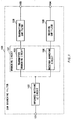
- Fig. 1 is the block diagram showing an example of the structure of the SAW branching filter described in the first embodiment of the present invention.
- the SAW branching filter 100 comprises of the antenna terminal 101, transmitting terminal 103 and receiving terminal 104.
- the impedance matching LC circuit 102 is connected to the antenna terminal 101.
- the transmitting side branching circuit (called the Tx-branching circuit from now on) 105 and the transmitting SAW filter 108 are connected between the impedance matching LC circuit 102 and the transmitting terminal 103.
- the receiving side branching circuit (called the Rx-branching circuit from now on) 106 and the receiving SAW filter 109 are connected between the impedance matching LC circuit 102 and the receiving SAW filter 109.
- the transmitting filter 108 and the receiving SAW filter 109 have different frequency passing band.
- the branching circuit 107 is constructed from the Tx-branching circuit 105 and the Rx-branching circuit 106, depending on the design requirements, Tx-branching circuit 105 does not have to be included.
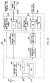
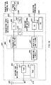
- Fig.2 and Fig.3 shows the concrete circuit structure diagram for the above SAW branching filter 100 which includes both the Tx-branching circuit 105 and the Rx-branching circuit 106.
- the transmitting SAW filter 108 comprises of a three stage ladder type SAW resonator made up from two serial arm SAW resonator and a parallel SAW resonator.
- the serial arm resonator consists of the first stage number 1 serial arm SAW resonator (TS1) 108a and the second stage number 2 serial arm SAW resonator (TS2) 108b, is connected between the Tx-branching circuit 105 and the transmitting terminal 103.
- the parallel arm SAW resonator consists of a) the first stage number 1 parallel arm SAW resonator (TP1) 108c, which is connected between the connection point of the first serial arm SAW resonator (TS1) 108a and the second serial arm SAW resonator (TS2) 108b, and the earth, b) the second stage number 2 parallel arm SAW resonator (TP2) 108d, which is connected between the transmitting terminal 103 and the earth.
- each serial arm SAW resonator and each parallel SAW resonator included in the transmitting SAW filter 108 comprises of two SAW resonators.
- the receiving SAW filter 109 comprises of a five stage ladder type SAW resonator made up from three serial arm SAW resonator and parallel arm SAW resonator.
- the serial arm SAW resonator is connected between the Rx-branching circuit 106 and receiving terminal 104, and consists of the first stage number 1 serial arm SAW resonator (RS1) 109a, the second stage number 2 serial arm SAW resonator (RS2)109b, and the third stage number 3 serial arm SAW resonator (RS3) 109c.
- the parallel arm SAW resonator consists of a) the first stage number 1 parallel arm SAW resonator (RP1) 109d which is connected between the connection point of the number 1 serial arm SAW resonator (RS1) 109a and number 2 serial arm SAW resonator (RS2) 109b, and the earth, b) the second stage number 2 parallel arm SAW resonator (RP2) 109e, which is connected between the connection point between the number 2 serial arm SAW resonator (RS2) 109b and the number 3 serial arm SAW resonator (RS3) 109c, and the earth, and c) the third stage number 3 parallel SAW resonator (RP3) 109f, which is connected between the transmitting terminal 104 and the earth.
- RP1 first stage number 1 parallel arm SAW resonator
- RS2 number 2 serial arm SAW resonator
- RS3 serial arm SAW resonator
- Tx-branching circuit 105 uses the serial arm type SAW resonator (T x S) 105a, and the Rx-branching circuit 106 uses the parallel SAW resonator (R x S) 106a.
- the impedance matching LC circuit 102 consists of capacitor C and Inductor L .
- the number 1 serial arm SAW resonator (TS1) 108a used by the transmitting SAW filter 108, and the serial arm SAW resonator (T x S) 105a of the Tx-branching circuit 105 are combined as a combination SAW resonator 108e.
- the number 1 serial arm SAW resonator (RS1) 109a used by the receiving SAW filter 109, and the parallel SAW resonator (R x S) 106a of the Rx-branching circuit 106 are combined to form the combined resonator 109g.
- Fig. 4A shows the perspective view of the package base board 111 which houses the piezo electric base board 110 on which the SAW branching filter 100 described above, consisting of the transmitting SAW filter 108 and the receiving SAW filter 109, is formed.
- the package base board resin base board, low temperature sintering based board, aluminum base board can be used.
- this package base board can be formed using multiple layered package base board. This will be described in detail in embodiment 2 to embodiment 4.
- Tx-in and Tx-out shown in Fig. 4A are the input terminal and the output terminal for the transmitting SAW filter 108 respectively.
- Rx-in and Rx-out are the input terminal and the output terminal for the receiving SAW filter 109.
- the output terminal of the transmitting SAW filter 108 and the input terminal of the receiving SAW filter 109 are not shown, they are both connected with the antenna terminal 101. Furthermore, the input terminal of the transmitting SAW filter 108 is related to the transmitting terminal 103 shown in Fig. 1, and the output terminal of the receiving SAW filter 109 is related to the receiving terminal 104 shown in Fig. 1 respectively.
- the branching circuit 107 and the frequency regulator LC element 102 are formed on the package base board 111, outside of the piezo electric base board 110.
- Fig. 4C shows the case in which the branching circuit 107, transmitting SAW filter 108, and the receiving SAW filter 109 are formed on the same piezo electric base board 110.
- the Tx-branching circuit 106 and the Rx-branching circuit 106 are included as branching circuit 107, both branching circuits should be housed on this piezo electric base board 110.
- the branching circuit 107 only includes the Rx-branching circuit 106, only the Rx-branching circuit 106 should be housed on the piezo electric base board 110.
- the necessary connection lines as well as the input and output terminals are omitted, and the Tx-branching circuit 105 is shown in dotted line, and the Rx-branching circuit 106 is shown in solid line.
- the impedance matching LC circuit 102 is housed outside of the piezo electric base board 110.
- Fig. 4C shows the case in which the impedance matching LC circuit 102, the branching circuit 107, the transmitting SAW filter 108 and the receiving SAW filter 109 are housed on the same piezo electric base board 110. Similar to the example shown in Fig. 4B, when the branching circuit includes the Tx-branching circuit 105 and the Rx-branching circuit, both branching circuits should be housed on the piezo electric base board 110.
- the Tx-branching circuit 105 is also housed according to the design described above. However, in Fig. 4C, the necessary connection circuits, and the input and output terminal are omitted.
- the Tx-branching circuit 105 and the Rx-branching circuit 106 which form the SAW branching filter 100, as shown in the above Fig. 4A to Fig. 4C, comprises of various serial arm SAW resonators.
- Fig. 5 shows the different functions of each components of the SAW branching filter 100 when it is activated for transmitting operation.
- Fig. 6 shows the different functions of each components of the SAW branching filter 100 when it is activated for receiving operations.
- Fig. 7 describes the impedance of the SAW branching filter 100.
- branching filter uses only one antenna. Therefore, when transmitting signal is transmitted and receiving signal is received, the antenna is shared by both sides and connected directly to both the transmitting related circuit and the receiving related circuits. Due to this reason, the performance of the branching filter has a very large impact on that of small mobile communication devices.
- the transmitting signal from the power amplifier 113 is sent to the transmitting SAW filter 108 through the transmitting terminal 103.
- the frequency band of the transmitting signal is first regulated by the transmitting SAW filter 108, and sent to antenna 112 via the antenna terminal 101, before it is transmitted.
- the receiving part circuit 114 which consists of the Rx-branching circuit 106, and the receiving SAW filter 109, together with antenna 112, can be viewed as a load circuit with a combined resistance R1.
- the signal received from antenna 112 is sent to the receiving SAW filter 109 via the antenna terminal 101.
- the frequency passing band of the received signal is regulated by the receiving SAW filter 109, and sent to the receiving part circuit 114 via the receiving terminal 104.
- the transmitting part circuit 115 which consists of the Tx-branching circuit 105 and the transmitting SAW filter 108, together with antenna 112, can be viewed as a load circuit with combined resistance P2.
- the SAW branching filter 100 during the transmitting operation and the receiving operation can be understood by study the diagrams shown in Fig. 5 and Fig. 6. As such, the SAW branching filter 100 must satisfy the following necessary conditions if it is to be considered as a high performance branching filter.
- the transmitting frequency band of mobile cellular phone is from 890MHz to 915Mhz, and the receiving frequency band to be from 935MHz to 960MHz, it is possible to set the receiving frequency passing band of the transmitting SAW filter 108, which is contained in the transmitting part circuit 115, to the hyper frequency range from 930MHz to 960 MHz, through the serial arm SAW resonator 108a and 108b. Due to this reason, the impedance of the transmitting SAW filter 108 can be made to satisfy the approximation equation (1-3).
- the transmitting frequency passing band of the receiving SAW filter 109 which is contained in the receiving part circuit 114, to the hyper frequency range of 890MHz to 915MHz, through the serial arm SAW resonator 109a to 109c.
- the input impedance of the receiving SAW filter 109 can not be made to satisfy the approximation equations (1-1) and (1-2).
- Fig. 8A shows the circuit diagram of the serial arm SAW resonator used by the SAW branching filter of the present invention.
- Fig. 8B is the LC equivalent circuit diagram of the serial arm SAW resonator shown in Fig. 8A.
- the branching filter described in the present convention has both transmitting SAW filter and the receiving SAW filter on the same piezo electric base board. Simulation to compare the impedance characteristic during the transmitting operation is conducted.
- the subject branching filters of this simulation are the SAW branching filter using the GSM type branching filter found in many mobile cellular phones.
- the GSM type branching filter does not contain the basic component Tx-branching circuit 105 and inductor L ANT but rather using the serial arm SAW resonator 106a as the Rx-branching circuit. Therefore, the frequencies used in this simulation are 890MHz, 915MHz, 935MHz, and 960MHz, within the range of 890MHz and 960MHz.
- the transmitting SAW filter for both the conventional branching filter and the GSM (Global System for Mobile communication) type branching filter used in the present invention are constructed in the same way as the transmitting SAW filter 108 shown in Fig. 2.
- Fig. 8 shows the cross length ( ⁇ m) and the electrode logarithm of the SAW resonator which forms the transmitting and receiving SAW filter in SAW branching filter 100.
- TS1 and TS2 are the serial arm SAW resonator 108a and 108b
- TP1 and TS2 are the parallel SAW resonator 108c and 108d, which form the transmitting SAW filter 108
- RS1 to RS3 are the serial arm SAW resonator 109a to 109c respectively
- RP1 and RP2 are the parallel arm SAW resonator 109d and 109e respectively, which form the receiving SAW filter 109.
- the branching filter used in the present invention are constructed using the serial arm SAW resonator 106a as the Rx-branching circuit 106.
- the conventional branching filter used in this simulation has the transmitting SAW filter and receiving SAW filter housed on different piezo electric base board.
- the Rx-branching circuit and the frequency regulating LC circuit are put on the package base board which carries the different piezo electric base board on which the transmitting SAW and the receiving SAW filter are formed.
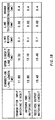
- Fig. 9 shows the type of branching filters, the required parameter and the impedance value of various branching circuit used to obtain the simulation results.
- symbol A and B denote branching filters with conventional construction
- symbol C to E denote branching filters constructed in the present invention.
- These branching filters are branching filters that uses SAW resonator and used for mobile cellular phones.
- the transmitting frequency band is from 890MHz to 915MHz
- the receiving frequency band is from 935MHz to 960MHz, which are used by the GSM type branching filter.
- the Tx-branching circuit 105 is not included as shown in the circuit diagram of Fig. 1. Therefore, the input terminal of the transmitting SAW filter is directly connected the impedance matching LC circuit 102.
- the serial arm SAW resonator 106a is included in the Rx-branching filter circuit 106.
- the serial arm SAW resonator 106a consists of the first stage serial arm SAW resonator 109a of the receiving SAW filter 109, and the combined resonator 109g.
- Fig. 10 the real part and the imaginary part of the input impedance Z r 117 and Z t 116 of the transmitting SAW filter 108 relating to both specific branching filter B (conventional) and branching filter D (the present invention) shown in Fig. 7, are shown respectively.
- the value of the input impedance of various transmitting and receiving SAW filter for frequencies of 890 MHz, 915 MHz, 935 MHz and 960 MHz are also shown.
- the unit of real part and the imaginary part values in Fig. 10 are ohms and standardized at 50 ohms.
- the input impedance Z r for the branching filter D of the present invention are 3.54 for the real part and 23.30 for the imaginary part.
- the branching filter of the present invention has improved the frequency characteristic to a very large extend.
- the transmitting frequency passing band is from 935 MHz to 960 MHz.
- the branching filter described in the present invention whose impedance characteristic was studied in the simulation, is the result of miniaturization due to the combining of the first stage serial arm SAW resonator of the receiving SAW filter in the Rx-branching circuit.
- the compound impedance Z in can be calculated according to equation (1-5).
- Z in Z t x Z r / (Z t + Z r )
- Z t (900) 0.863 - j0.626
- Z t (900) 0.0175 - j0.934
- the impedance Z in can be obtained from equation (1-8).
- Z in (Tr) (900) 0.2409 - j0.501
- Fig. 9 shows the results of impedance adjustment using only the inductor L ANT 102b at the transmitting frequency band range from 890 MHz to 915 MHz for branching filter D and E.
- the results of impedance adjustment using both inductor L ANT 102b and capacitor C ANT 102a at transmitting frequency band range from 890 MHz to 915 MHz for branching filter C.
- the characteristic of frequency passing band of the SAW branching filter can be improved using the impedance matching LC circuit 102 housed out side of the module.
- the transmitting SAW filter and the receiving SAW filter are formed on the same piezo electric base board, when dicing the transmitting and receiving SAW filter 108 and 109 in wafer conditions, it is not necessary to separate the transmitting SAW filter 108 and the receiving SAW filter 109.
- the impedance at the transmitting band range of the receiving SAW filter 109 becomes much larger due to the fact that the serial arm SAW resonator 106a is used for the branching circuit.
- This improvement is dependent on the impedance looking from the filter side at point C 118 as shown in Fig. 7. That is to say, it can be considered as the consequences of inserting the serial arm SAW resonator 106a in the input terminal of the receiving SAW filter 109 as the branching circuit.
- the frequency regulating LC circuit into a chip and house it on the transmitting and receiving filter package base board, or house it on the piezo electric base board on which the transmitting and receiving SAW filter are formed, it is possible to achieve further miniaturization and higher performance for branching filters which contains SAW resonators.
- the second to fourth embodiment of the present invention is explained using Fig. 9 to Fig. 12.
- Fig. 9 shows the structure diagram of the SAW branching filter 200 as described in the second embodiment of the present invention.
- the transmitting and receiving SAW filter 206 and 207 are formed on the same piezo electric base board 208.
- the multi layered package base board which houses the SAW branching filter described in the second embodiment is shown in Fig. 12A to Fig. 12C.
- the SAW branching filter 200 described in the second embodiment is constructed as follows. First, as shown in Fig. 9, the transmitting SAW filter 206 and the receiving SAW filter 207 are formed on the same piezo electric base board 208.
- the antenna terminal matching circuit 202 and the branching circuit 205 are located between the receiving SAW filter 207 and the antenna terminal 201, which is connected to antenna 221.
- the antenna terminal matching circuit 202 consists of a strip line L ANT 216 used as an inductor, and the open stab S ANT 217 used as a capacitor.
- the antenna matching circuit 202 is connected to the earth via terminal 218.
- the transmitting terminal 203 is connected to the output terminal of power amplifier 215 and the transmitting input matching circuit 213 is connected between the transmitting terminal 203 and the transmitting SAW filter 206.
- the transmitting input matching circuit 213 consists of a strip line L r 209 used as an inductor and a open stab S r 210 used as a capacitor.
- the transmitting input matching circuit 213 is connected to the earth via terminal 219.
- the receiving output matching circuit 214 is connected between the receiving terminal 204 and the receiving SAW filter 207.
- the receiving output matching circuit 214 consists of a strip line L R 211 as a inductor and a open stab S R 212 as a capacitor.
- the receiving output matching circuit 214 is connected to the earth via terminal 220.
- the multi layer package base board described in the present invention basically consists of package base board 600 to 800 as shown in Fig. 12A to Fig. 12C.
- a cavity 601 is located in order to provide space for the housing of peizo electric base board 208, which in turn is used to house the transmitting SAW filter 206 and 207.
- the electrode pad 602A to 602H, the transmitting terminal 603A, antenna terminal 603B, and the receiving terminal 603C are formed on package base board 600.
- the strip line 605 which is equivalent to the strip line L r 209 of the transmitting input matching circuit 213 is formed between the transmitting terminal 603A and the electrode pad 602H.
- the electrode pad 602H is connected to the terminal 806 in the multi layer package base board.
- the terminal 806 on package base board 800 is connected with the open stab 805, which in turn corresponds to the open stab ST210.
- the input terminal of the transmitting SAW filter 206 is connected to electrode pad 602H via methods such as wire bonding.
- the strip line 606A which is equivalent to the strip line L ANT 216 of the antenna matching circuit 202, is formed between the antenna terminal 603B and the electrode 602D.
- the antenna terminal 603B is connected to the output terminal of the transmitting SAW filter 206, via terminal 607, wiring 606B and electrode terminal 602D.
- terminal 607 is connected to terminal 803, and connected to terminal 804 via the branching circuit 801 which corresponds to branching circuit 205.
- Terminal 804 is connected to the electrode pad 602A located in the multi layer package base board, and the electrode pad 602A is further connected to the input terminal of the receiving SAW filter 207 using techniques such as wire bonding.
- the antenna terminal 603B is connected to terminal 802B of the package base board 800 located in the multi layer package base board.
- the open stab 807 which corresponds to open stab S ANT 217 of the antenna matching circuit 202 is formed on the package base board 800.
- the receiving terminal 603C is connected to terminal 802C in the multi layer package base board.
- the open stab 808 corresponds to open stab S R 212 is further formed in terminal 802C.
- the electrode pads 602C and 602G located on the package base board 600 are connected to terminal 701A and 701B that are located on the package base board 700 in the multi layer package base board.
- terminal 701A and 701B is located in the ground voltage pattern 701 which is connected to the ground voltage V SS via terminal 703A to 703C and 703H.
- the electrode pad 602C and 602G located in the package base board 600 is used as ground electrode pad.
- the electrode pad 602C is used as the ground voltage electrode pad 218 in the antenna terminal matching circuit 202
- the electrode pad 602G is used as ground voltage electrode pad 219 in the receiving input matching circuit 213.
- the electrode pads 602B and 602F located in the package base board 600 are connected to terminal 702A and 702B of the package base board 700 in the multi layer package base board.
- terminal 702A and 702B are located in the ground voltage pattern 702 which is connected to the ground voltage V SS via terminal 703D to 703G.
- the electrode pad 602B and 602F located in the package base board 600 is used as ground electrode pads.
- the electrode pad 602B is used as the ground voltage electrode pad 218 in the antenna terminal matching circuit 202
- the electrode pad 602F is used as ground voltage electrode pad 220 in the receiving input matching circuit 214.
- the piezo electric base board 208 on which the transmitting and receiving SAW filter 206 and 207 are formed, is housed in the chip housing area 704 on package base board 700.
- the ground voltage pattern 702 of the chip housing area 704 multiple through holes are provided. These through holes 705 are connected to the multiple through holes 809 located on the package base board 800 of the multi layer package base board.
- the transmitting SAW filter 206 and the receiving SAW filter 207 are formed on the same piezo electric base board 208.
- the piezo electric base board 208 By housing the piezo electric base board 208 on multi layer package base board, it is possible to achieve further miniaturization of the SAW branching filter.
- the strip line L r 209 (605) , L R 211 (608) and L ANT (606A) are formed on package base board 600, and the branching circuit 205 (801), open stab ST 210 (805), SR 212 (808) and SANT 217 (807) are formed on package base board 800.
- the strip line is formed on the branching circuit while the open stab is formed on other package base board the SAW branching filter as a whole can be further miniaturized.
- through hole 705 and 809 are arranged in the housing area to be used to house the piezo electric base board forming the transmitting SAW filter 206 and 207 in package base board 700 and 800, it is possible to radiate the heat generated from the transmitting and receiving SAW filter 206 and 207 efficiently. As such, the reliability of the SAW branching filter is improved.
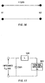
- Z O is the characteristic impedance of the connection circuit
- LL is the connection length (cm)
- CC 3.0 x 10 10 .
- the impedance Z ln of the branching circuit or the SAW filter including connection circuit shown in Fig. 14 can be calculated using equation (2-3).
- Z in (Z n + jWL) / (1+jWC(Z n + jWL))
- the impedance value Z in of SAW branching filter can be set as expected via the use of connection lines such as strip lines.
- the impedance in branching circuit 2.5 it is possible to have circuit with even lower loss by setting the impedance in branching circuit 2.5 to lower value.
- the characteristic impedance of the branching circuit in SAW branching filter 200 can be set to 40.2 ohm, achieve lower SAW branching filter loss.
- the open circuit (open stab S r 210) of the transmitting input matching circuit 213 in the second embodiment is explained concretely.
- the equivalent capacity C inf is 2.63 pF.
- Fig. 10 shows the structure diagram of the SAW branching filter 300 described by the third embodiment of the present invention.
- the branching circuit 305, transmitting SAW filter 306 and the receiving SAW filter 307 are formed on one piezo electric base board 308.
- the multi layer package base board which is used to house the SAW branching filter is explained through Fig. 12 (A) to Fig. 12 (C).
- the SAW branching filter 300 described in the third embodiment is constructed as follows. First, as shown in Fig. 10, the branching circuit 305, transmitting SAW filter 306, and receiving SAW filter 307 is formed on a single piezo electric base board 308. The branching circuit 305 is located between the antenna terminal 301, which is linked to antenna 321, and the receiving SAW filter 307. The antenna terminal matching circuit 303 is located between the antenna terminal 301 and the branching circuit 305.
- the antenna terminal matching circuit 302 consists of the strip line L ANT 316 used as an inductor and the open stab S ANT 317 used as a capacity. In addition, the antenna terminal matching circuit 302 is linked earth via terminal 318.
- the transmitting terminal 303 is connected t the output terminal of the power amplifier 315.
- the transmitting input matching circuit 313 is connected between the transmitting terminal 303 and the transmitting SAW filter 306.
- the transmitting input matching circuit 313 consists of the strip line L r 309 used as an inductor and the open stab S r 310 used as a capacity.
- the transmitting input matching circuit 313 is connected to the earth via terminal 319.
- the receiving output matching circuit 314 is connected between the receiving terminal 304 and the receiving SAW filter 307.
- the receiving output matching circuit 314 consists of the strip line L R 311 used as an inductor, and the open stab S R used as a capacitor.
- the receiving output matching circuit 314 is connected to the earth vial terminal 321.
- Fig. 12 shows the structure of SAW branching filter 300 described above when housed on a multi layer package base board and is explained as follows.
- the multi layer package base board described in the present invention, in foundation, is derived from the package base board 600 to 800.
- space and cavity 601 is formed to house the piezo electric base board 308 of the receiving SAW filter 306 and 307. Furthermore, the electrode pad 602A to 602H, transmitting terminal 603A, and antenna terminal 603A, atenna terminal 603B and receiving terminal 602C are formed on the package base board 600.
- the strip line 605 corresponding to the strip line L r 309 of the transmitting input matching circuit 313 is formed between the transmitting terminal 603A and the electrode pad 602H.
- the open stab 604 is connected to the transmitting terminal 603A in package base board 600, there is no need for such arrangement in embodiment 3.
- electrode pad 602H is connected to terminal 806 in side the multi layer package base board, and this terminal 806 is connected to the open stab 805 which corresponds to the open stab ST 310 in package base board 800.
- the electrode pad 602H is connected to the input terminal of the transmitting SAW filter 306 using wire bonding method.
- the strip line 606A which corresponds to strip line L ANT 316 of the antenna matching circuit 302, is connected between the antenna terminal 603B and the electrode pad 602D.
- the antenna terminal 603B is further connected to the output terminal of the transmitting SAW filter 306 via terminal 607, circuit 606B and electrode terminal 602D.
- the branching circuit 305 is formed on piezo electric base board 308 along with the transmitting and receiving SAW filter, there is no need to include branching circuit 601 similar to those shown in Fig. 12C.
- antenna terminal 603B is connected to terminal 802B of the package base board 800 in the multi layer package base board, and the open stab 807 which corresponds to the open stab S ANT 317 antenna end matching circuit 302 is formed in this package base board 800.
- the receiving terminal 603C is connected to terminal 802C in side the multi layer package base board.
- the open stab 808 corresponding to open stab S R 312 is formed in terminal 802C.
- the electrode pad 602C and 602G in package base board 600 are lined to terminal 701A and 701B of the package base board 700 in the multi layer package board 700 respectively.
- terminals 701A and 701B is set up in the earth voltage pattern 701 connected to the earth voltage V SS through terminal 703A to 703C and 703H.
- the electrode pad 602C and 602G in the package base board 600 can be used as earth voltage electrode pad.
- the electrode pad 602C is used as the earth voltage electrode pad 318 in antenna terminal matching circuit 302, and the electrode pad 602G is used as the earth voltage electrode pad 319 in the transmitting input matching circuit 313.
- the electrode pad 602B and 602F in package base board 600 are connected to terminal 702A and 702B in package base board 700 of the multi layer package board.
- terminals 702A and 702B are set up in side the earth voltage pattern 702 connected to the earth voltage V SS via terminal 703D to 703G respectively.
- the electrode pad 602B and 602F in package base board 600 are used as earth voltage electrode pads.
- the electrode pad 602B is used as earth voltage electrode pad 318 in antenna end matching circuit 302
- electrode pad 602F is used as the earth voltage electrode pad 320 in the receiving output matching circuit 314.
- the branching circuit 305, transmitting and receiving SAW filter 306 and 307 are formed on the piezo electric base board 308, housed on the chip housing area 704 on package base board 700.
- multiple through holes 705 are set up in the chip housing area 704 of earth voltage pattern 702, which through holes 705 are connected to the multiple through holes set up in the package base board 800 of the multi layer package base board.
- the branching filter circuit 305, transmitting SAW filter 306 and receiving SAW filter 307 are formed on a single piezo electric base board 308. Furthermore, the piezo electric base board 308 is housed in the multi layer package base board, thus enable further miniaturization of the whole SAW branching filter. Still more, the strip line L r 309 (605), L R 311 (608) and L ANT 316 (606A) are formed on package base board 700. On the other hand, open stab S r 310 (805), S R 312 (808) and S ANT 317 (807) are formed on package base board 800.
- the strip line are formed along with the branching circuit and the open stab on different package base board, thus achieving further miniaturization for the whole branching filter.
- the branching circuit 305 is formed on piezo electric base board 308 with small loss, it is possible to improve the frequency characteristic of SAW branching filter 300.
- the transmitting input matching circuit 313 and the receiving output matching circuit 314 and their related earth voltage pattern are separately setup, it is possible to control the worsening of the frequency characteristic of the SAW branching filter due to the interference between the transmitting SAW filter 306 and the receiving SAW filter 307.
- through hole 705 and 809 are setup in the housing area which is used to house the piezo electric base board forming the transmitting and receiving SAW filter 306 and 307 on package base board 700 and 800, it is possible to radiate the heat generated from the transmitting and receiving SAW filter 306 and 307 efficiently to the outside, and further improve the reliability of the SAW branching filter 300.
- Fig. 11 shows the structure diagram of the SAW branching filter 400 described in the fourth embodiment of the present invention.
- the transmitting SAW filter 406 and the receiving SAW filter 407 are formed on a single piezo electric base board 408.
- the multi layer package base board used to house the SAW branching filter are explained using Fig. 12A to Fig. 12C.
- the SAW branching filter 400 described in the fourth embodiment of the present invention as constructed as follows. First, as shown in Fig. 11, the transmitting SAW filter 406 and the receiving SAW filter 407 are formed on a single piezo electric base board 408.
- the antenna end matching circuit 402 and branching circuit 405 are set up between the receiving SAW filter 407 and the antenna terminal 401 connected to antenna 422.
- the antenna end matching circuit 402 consists of the strip line L ANT 417 used as an inductor, and the open stab S ANT 418 used as a capacitor.
- the antenna end matching circuit 402 is connected to the earth via terminal 419.
- the transmitting terminal 403 is connected to the output terminal of the power amplifier 416.
- the transmitting input matching circuit 412 is connected between the transmitting terminal 403 and the transmitting SAW filter 406.
- the transmitting input matching circuit 412 consists of the strip line L r 409 used as an inductor and open stab S r 410 used as a capacity, and S rs 411.
- the transmitting input matching circuit 412 is connected to the earth via terminal 420.
- l is the length of the open stab (mm)
- c the speed of light (300 x 10 6 m/s)
- f the frequency to be eliminated
- er is the specific inductive capacity.
- the receiving output matching circuit 415 is connected between the receiving terminal 404 and receiving SAW filter 407.
- the receiving output matching circuit 415 consists of strip line L R 413 used as an inductor and the open stab S R 414 used as a capacitor.
- the receiving output matching circuit 415 is connected to the earth via terminal 412.
- the SAW branching filter 400 constructed as described above when housed on the multi layer package base board is explained as follows.
- the multi layer package base board described in the present invention basically consists of boards similar to package base board 600 to 800.
- space and cavity 601 is formed to house the piezo electric base board 408 of the receiving SAW filter 406 and 407. Furthermore, the electrode pad 602A to 602H, transmitting terminal 603A, and antenna terminal 603B, atenna terminal 603B and receiving terminal 603C are formed on the package base board 600.
- the strip line 605 corresponding to strip line L r 409 of the receiving input matching circuit 412 is formed between the transmitting terminal 603A and the electrode pad 602H.
- the transmitting terminal 603A is connected to open stab 604 corresponding to open stab S RS 411 on package base board 600.
- electrode pad 602H is connected to terminal 806 of the multi layer package base board.
- the open stab 805 corresponding to open stab S r 410 is connected to this terminal 806 in the package base board 800.
- the input terminal of the transmitting SAW filter 406 is connected to the electric pad 602H using wire bonding methods.
- terminal 607 is connected to terminal 803, and connected to terminal 804 via the branching circuit 801 corresponding to branching circuit 405, and the electrode pad 602A is connected to the input terminal of the receiving filter 407 using wire bonding methods.
- the strip line 606A which corresponds to the strip line L ANT 417 of the antenna end matching circuit 402, is connected between the antenna terminal 603B and the electrode pad 602D.
- Antenna terminal 603B is connected to the output terminal of the transmitting SAW filter 406 via terminal 607, circuit 606B and electrode terminal 602D.
- the antenna terminal 603B is connected to terminal 802B of the package base board 800 in the multi layer package base board.
- the open stab 807 corresponding to the open stab S ANT 418 of the atenna end matching circuit 402 is also formed in this package base board 800.
- the receiving terminal 603 is connected to terminal 802C in side of the multi layer package base board.
- open stab 808 corresponding to open stab S R 414 is formed in terminal 802C.
- the electrode pad 602C and 602G in the package base board 600 are connected to terminal 701A and 701B of the package base board 700 respectively.
- terminals 701A and 701B are set up in the earth voltage pattern 701 connected to the earth voltage V SS via terminal 703A to 703C and 703H.
- the electrode pads 602C and 602G in package base board 600 can be used as earth voltage electrode pads.
- the electrode pad 602C is used as earth voltage electrode 419 in the antenna end matching circuit 402
- the electrode pad 602G is used as the earth voltage electrode pad 420 in the transmitting input matching circuit 412.
- the electrode pads 602B and 602F in the package base board 600 are connected to terminal 702A and 702B of the package base board 700 in the multi layer package base board.
- terminals 702A and 702B are set up in the earth voltage pattern 702 connected to the earth voltage V SS via terminal 703D to 703D.
- the electrode pads 602B and 602F in package base board 600 can be used as earth voltage electrode pads.
- the electrode pad 602B is used as earth voltage electrode 420 in the antenna end matching circuit 402
- the electrode pad 602F is used as the earth voltage electrode pad 421 in the transmitting input matching circuit 415.
- the branching circuit 405, transmitting and receiving SAW filter 406 and 407 are formed on the piezo electric base board 408, housed on the chip housing area 704 on package base board 700.
- multiple through holes 705 are setup. These through holes 705 are connected to the multiple through holes 809 set up in the package base board 800 of the multi layer package base board.
- the branching filter circuit 405, transmitting SAW filter 406 and receiving SAW filter 407 are formed on a single piezo electric base board 408. Furthermore, the piezo electric base board 408 is housed in the multi layer package base board, thus enable further miniaturization of the whole SAW branching filter. Still more, the strip line Lr 409 (605), L R 413 (608) and L ANT 417 (606A) are formed on package base board 700. On the other hand, open stab S r 410 (805), S R 414 (808) and S ANT 418 (807) are formed on package base board 800. That is to say, the strip line are formed along with the branching circuit and the open stab on different package base board, thus achieving further miniaturization for the whole branching filter.
- the transmitting input matching circuit 412 and the receiving output matching circuit 415 and their related earth voltage pattern are separately setup, it is possible to control the worsening of the frequency characteristic of the SAW branching filter due to the interference between the transmitting SAW filter 406 and the receiving SAW filter 407.
- through hole 705 and 809 are setup in the housing area which is used to house the piezo electric base board forming the transmitting and receiving SAW filter 406 and 407 on package base board 700 and 800, it is possible to radiate the heat generated from the transmitting and receiving SAW filter 406 and 407 efficiently to the outside, and further improve the reliability of the SAW branching filter 400.
- the open stab S rs 411 is set up in the transmitting input matching circuit 412, it is possible to set the spurious band attenuation in the SAW branching filter 400 to expected value.
Landscapes
- Physics & Mathematics (AREA)
- Acoustics & Sound (AREA)
- Surface Acoustic Wave Elements And Circuit Networks Thereof (AREA)
Abstract
Description

Claims (7)
- A branching filter package (100) comprising:a SAW filter chip housing area which houses a piezo electric base, on which a transmitting SAW filter (108) and a receiving SAW filter (109) having a different frequency passing band with each other, are formed;an impedance matching circuit (102) for said transmitting SAW filter (108) and said receiving SAW filter (109); anda branching circuit (107) for said transmitting SAW filter and said receiving SAW filter.
- A branching filter package as claimed in claim 1, wherein said impedance matching circuit (102) is formed by using a strip line circuit and an open circuit.
- A branching filter package as claimed in claim 2 further comprising:a first package base board and a second package base board, wherein said strip circuit is formed on said first package base board, and said open circuit and said branching circuit (107) are formed on said second package base board.
- A branching filter package as claimed in claim 2, wherein said branching circuit (107) has a characteristic impedance lower than 50 ohm.
- A branching filter package as claimed in one of claims 1 to 4 further comprising:a plurality of package base board, wherein an earth voltage pattern for said transmitting SAW filter (108) and said receiving filter (109) is formed separately on one of said plurality of package base boards.
- A branching filter package as claimed in one of claims 1 to 5 further comprising:a heat radiating opening which radiates a heat generated from said transmitting SAW filter (108) and said receiving SAW filter (109) out of said branching filter package.
- A branching filter package as claimed in one of claims 1 to 6 further comprising:a plurality of package base boards,
wherein a spurious eliminating open stab, which is used as said impedance matching circuit, is formed on one of said plurality of package base boards.
Applications Claiming Priority (2)
| Application Number | Priority Date | Filing Date | Title |
|---|---|---|---|
| JP11149959A JP2000068785A (en) | 1998-06-09 | 1999-05-28 | Duplexer and duplexer package |
| JP14995999 | 1999-05-28 |
Publications (2)
| Publication Number | Publication Date |
|---|---|
| EP1056201A2 true EP1056201A2 (en) | 2000-11-29 |
| EP1056201A3 EP1056201A3 (en) | 2008-02-20 |
Family
ID=15486352
Family Applications (1)
| Application Number | Title | Priority Date | Filing Date |
|---|---|---|---|
| EP00105052A Withdrawn EP1056201A3 (en) | 1999-05-28 | 2000-03-09 | Branching filter package |
Country Status (2)
| Country | Link |
|---|---|
| EP (1) | EP1056201A3 (en) |
| KR (2) | KR100746065B1 (en) |
Cited By (1)
| Publication number | Priority date | Publication date | Assignee | Title |
|---|---|---|---|---|
| WO2014179693A1 (en) * | 2013-05-03 | 2014-11-06 | Rfaxis, Inc. | Coupled resonator on-die filters for wifi applications |
Families Citing this family (3)
| Publication number | Priority date | Publication date | Assignee | Title |
|---|---|---|---|---|
| JP3900013B2 (en) * | 2001-07-30 | 2007-04-04 | 株式会社村田製作所 | Surface acoustic wave duplexer, communication device |
| JP4000960B2 (en) * | 2001-10-19 | 2007-10-31 | 株式会社村田製作所 | Duplexer, communication equipment |
| KR20030067901A (en) * | 2002-02-08 | 2003-08-19 | 텔레포스 주식회사 | Surface acoustic wave duplexer |
Family Cites Families (8)
| Publication number | Priority date | Publication date | Assignee | Title |
|---|---|---|---|---|
| JP3337073B2 (en) * | 1990-05-09 | 2002-10-21 | 株式会社村田製作所 | Surface acoustic wave device |
| JPH0716427A (en) * | 1993-06-22 | 1995-01-20 | Kaoru Umeya | Air purifier |
| JPH07226607A (en) * | 1994-02-10 | 1995-08-22 | Hitachi Ltd | Demultiplexer, demultiplexer module, and wireless communication device |
| JP3487692B2 (en) * | 1995-10-02 | 2004-01-19 | 富士通株式会社 | Duplexer |
| JPH10233648A (en) | 1997-02-21 | 1998-09-02 | Oki Electric Ind Co Ltd | Duplexer |
| JPH10322105A (en) | 1997-05-19 | 1998-12-04 | Oki Electric Ind Co Ltd | Duplexer |
| JP4331277B2 (en) | 1997-08-22 | 2009-09-16 | 日本無線株式会社 | Surface acoustic wave filter |
| JP2000068785A (en) * | 1998-06-09 | 2000-03-03 | Oki Electric Ind Co Ltd | Duplexer and duplexer package |
-
2000
- 2000-03-08 KR KR1020000011583A patent/KR100746065B1/en not_active Expired - Lifetime
- 2000-03-09 EP EP00105052A patent/EP1056201A3/en not_active Withdrawn
-
2007
- 2007-03-27 KR KR1020070029999A patent/KR100759737B1/en not_active Expired - Fee Related
Cited By (3)
| Publication number | Priority date | Publication date | Assignee | Title |
|---|---|---|---|---|
| WO2014179693A1 (en) * | 2013-05-03 | 2014-11-06 | Rfaxis, Inc. | Coupled resonator on-die filters for wifi applications |
| US9853620B2 (en) | 2013-05-03 | 2017-12-26 | Skyworks Solutions, Inc. | Coupled-resonator on-die filters for WiFi applications |
| US10516379B2 (en) | 2013-05-03 | 2019-12-24 | Skyworks Solutions, Inc. | Coupled resonator on-die filters for WiFi applications |
Also Published As
| Publication number | Publication date |
|---|---|
| EP1056201A3 (en) | 2008-02-20 |
| KR20070039025A (en) | 2007-04-11 |
| KR20010006758A (en) | 2001-01-26 |
| KR100746065B1 (en) | 2007-08-03 |
| KR100759737B1 (en) | 2007-09-20 |
Similar Documents
| Publication | Publication Date | Title |
|---|---|---|
| US7893794B2 (en) | Branching filter package | |
| US5554960A (en) | Branching filter, branching filter module and radio commnication apparatus | |
| US7941103B2 (en) | Duplexer | |
| JP3855842B2 (en) | Surface acoustic wave duplexer and communication apparatus having the same | |
| CN1663120B (en) | Electronic component comprising a multilayer substrate | |
| US7515879B2 (en) | Radio frequency circuit module | |
| US7053731B2 (en) | Duplexer using surface acoustic wave filters | |
| US6870440B2 (en) | Saw branching filter with a branching filter circuit formed on the package | |
| US9941859B2 (en) | Ladder-type filter, duplexer, and module | |
| KR100624554B1 (en) | Antenna switch circuit, and composite high frequency part and mobile communication device using the same | |
| EP1804377A2 (en) | SAW filter and portable terminal | |
| JP2000068785A (en) | Duplexer and duplexer package | |
| KR100759737B1 (en) | Branching filter package | |
| JPH08191230A (en) | Duplexer | |
| JP2008067413A (en) | Branching filter | |
| JP2003152590A (en) | Antenna switch module | |
| JP2008104219A (en) | Branching filter | |
| US6069541A (en) | High-frequency filter, with an inductor for forming a pole, complex electronic component using the same, and portable radio apparatus using the same | |
| US7106150B2 (en) | Surface acoustic wave filter | |
| JP2005168049A (en) | Branching filter | |
| JPH0818306A (en) | Dielectric filter | |
| JP2003163569A (en) | Antenna duplexer package | |
| JP2005136888A (en) | High frequency demultiplexing circuit, high frequency component, high frequency module and wireless communication device equipped with the same | |
| EP0944167A2 (en) | High-frequency filter, complex electronic component using the same, and portable radio apparatus using the same | |
| JP2006279554A (en) | High frequency module and wireless communication device using the same |
Legal Events
| Date | Code | Title | Description |
|---|---|---|---|
| PUAI | Public reference made under article 153(3) epc to a published international application that has entered the european phase |
Free format text: ORIGINAL CODE: 0009012 |
|
| AK | Designated contracting states |
Kind code of ref document: A2 Designated state(s): AT BE CH CY DE DK ES FI FR GB GR IE IT LI LU MC NL PT SE |
|
| AX | Request for extension of the european patent |
Free format text: AL;LT;LV;MK;RO;SI |
|
| PUAL | Search report despatched |
Free format text: ORIGINAL CODE: 0009013 |
|
| AK | Designated contracting states |
Kind code of ref document: A3 Designated state(s): AT BE CH CY DE DK ES FI FR GB GR IE IT LI LU MC NL PT SE |
|
| AX | Request for extension of the european patent |
Extension state: AL LT LV MK RO SI |
|
| 17P | Request for examination filed |
Effective date: 20080806 |
|
| 17Q | First examination report despatched |
Effective date: 20080922 |
|
| AKX | Designation fees paid |
Designated state(s): DE FR GB |
|
| STAA | Information on the status of an ep patent application or granted ep patent |
Free format text: STATUS: THE APPLICATION IS DEEMED TO BE WITHDRAWN |
|
| 18D | Application deemed to be withdrawn |
Effective date: 20091105 |