EP1055746A1 - Method of chemical vapor depositing tungsten films - Google Patents
Method of chemical vapor depositing tungsten films Download PDFInfo
- Publication number
- EP1055746A1 EP1055746A1 EP00304055A EP00304055A EP1055746A1 EP 1055746 A1 EP1055746 A1 EP 1055746A1 EP 00304055 A EP00304055 A EP 00304055A EP 00304055 A EP00304055 A EP 00304055A EP 1055746 A1 EP1055746 A1 EP 1055746A1
- Authority
- EP
- European Patent Office
- Prior art keywords
- gas flow
- per minute
- tungsten
- standard cubic
- centimeters per
- Prior art date
- Legal status (The legal status is an assumption and is not a legal conclusion. Google has not performed a legal analysis and makes no representation as to the accuracy of the status listed.)
- Withdrawn
Links
Images
Classifications
-
- C—CHEMISTRY; METALLURGY
- C23—COATING METALLIC MATERIAL; COATING MATERIAL WITH METALLIC MATERIAL; CHEMICAL SURFACE TREATMENT; DIFFUSION TREATMENT OF METALLIC MATERIAL; COATING BY VACUUM EVAPORATION, BY SPUTTERING, BY ION IMPLANTATION OR BY CHEMICAL VAPOUR DEPOSITION, IN GENERAL; INHIBITING CORROSION OF METALLIC MATERIAL OR INCRUSTATION IN GENERAL
- C23C—COATING METALLIC MATERIAL; COATING MATERIAL WITH METALLIC MATERIAL; SURFACE TREATMENT OF METALLIC MATERIAL BY DIFFUSION INTO THE SURFACE, BY CHEMICAL CONVERSION OR SUBSTITUTION; COATING BY VACUUM EVAPORATION, BY SPUTTERING, BY ION IMPLANTATION OR BY CHEMICAL VAPOUR DEPOSITION, IN GENERAL
- C23C16/00—Chemical coating by decomposition of gaseous compounds, without leaving reaction products of surface material in the coating, i.e. chemical vapour deposition [CVD] processes
- C23C16/06—Chemical coating by decomposition of gaseous compounds, without leaving reaction products of surface material in the coating, i.e. chemical vapour deposition [CVD] processes characterised by the deposition of metallic material
-
- C—CHEMISTRY; METALLURGY
- C23—COATING METALLIC MATERIAL; COATING MATERIAL WITH METALLIC MATERIAL; CHEMICAL SURFACE TREATMENT; DIFFUSION TREATMENT OF METALLIC MATERIAL; COATING BY VACUUM EVAPORATION, BY SPUTTERING, BY ION IMPLANTATION OR BY CHEMICAL VAPOUR DEPOSITION, IN GENERAL; INHIBITING CORROSION OF METALLIC MATERIAL OR INCRUSTATION IN GENERAL
- C23C—COATING METALLIC MATERIAL; COATING MATERIAL WITH METALLIC MATERIAL; SURFACE TREATMENT OF METALLIC MATERIAL BY DIFFUSION INTO THE SURFACE, BY CHEMICAL CONVERSION OR SUBSTITUTION; COATING BY VACUUM EVAPORATION, BY SPUTTERING, BY ION IMPLANTATION OR BY CHEMICAL VAPOUR DEPOSITION, IN GENERAL
- C23C16/00—Chemical coating by decomposition of gaseous compounds, without leaving reaction products of surface material in the coating, i.e. chemical vapour deposition [CVD] processes
- C23C16/02—Pretreatment of the material to be coated
- C23C16/0272—Deposition of sub-layers, e.g. to promote the adhesion of the main coating
-
- C—CHEMISTRY; METALLURGY
- C23—COATING METALLIC MATERIAL; COATING MATERIAL WITH METALLIC MATERIAL; CHEMICAL SURFACE TREATMENT; DIFFUSION TREATMENT OF METALLIC MATERIAL; COATING BY VACUUM EVAPORATION, BY SPUTTERING, BY ION IMPLANTATION OR BY CHEMICAL VAPOUR DEPOSITION, IN GENERAL; INHIBITING CORROSION OF METALLIC MATERIAL OR INCRUSTATION IN GENERAL
- C23C—COATING METALLIC MATERIAL; COATING MATERIAL WITH METALLIC MATERIAL; SURFACE TREATMENT OF METALLIC MATERIAL BY DIFFUSION INTO THE SURFACE, BY CHEMICAL CONVERSION OR SUBSTITUTION; COATING BY VACUUM EVAPORATION, BY SPUTTERING, BY ION IMPLANTATION OR BY CHEMICAL VAPOUR DEPOSITION, IN GENERAL
- C23C16/00—Chemical coating by decomposition of gaseous compounds, without leaving reaction products of surface material in the coating, i.e. chemical vapour deposition [CVD] processes
- C23C16/06—Chemical coating by decomposition of gaseous compounds, without leaving reaction products of surface material in the coating, i.e. chemical vapour deposition [CVD] processes characterised by the deposition of metallic material
- C23C16/08—Chemical coating by decomposition of gaseous compounds, without leaving reaction products of surface material in the coating, i.e. chemical vapour deposition [CVD] processes characterised by the deposition of metallic material from metal halides
- C23C16/14—Deposition of only one other metal element
-
- C—CHEMISTRY; METALLURGY
- C23—COATING METALLIC MATERIAL; COATING MATERIAL WITH METALLIC MATERIAL; CHEMICAL SURFACE TREATMENT; DIFFUSION TREATMENT OF METALLIC MATERIAL; COATING BY VACUUM EVAPORATION, BY SPUTTERING, BY ION IMPLANTATION OR BY CHEMICAL VAPOUR DEPOSITION, IN GENERAL; INHIBITING CORROSION OF METALLIC MATERIAL OR INCRUSTATION IN GENERAL
- C23C—COATING METALLIC MATERIAL; COATING MATERIAL WITH METALLIC MATERIAL; SURFACE TREATMENT OF METALLIC MATERIAL BY DIFFUSION INTO THE SURFACE, BY CHEMICAL CONVERSION OR SUBSTITUTION; COATING BY VACUUM EVAPORATION, BY SPUTTERING, BY ION IMPLANTATION OR BY CHEMICAL VAPOUR DEPOSITION, IN GENERAL
- C23C16/00—Chemical coating by decomposition of gaseous compounds, without leaving reaction products of surface material in the coating, i.e. chemical vapour deposition [CVD] processes
- C23C16/44—Chemical coating by decomposition of gaseous compounds, without leaving reaction products of surface material in the coating, i.e. chemical vapour deposition [CVD] processes characterised by the method of coating
- C23C16/458—Chemical coating by decomposition of gaseous compounds, without leaving reaction products of surface material in the coating, i.e. chemical vapour deposition [CVD] processes characterised by the method of coating characterised by the method used for supporting substrates in the reaction chamber
- C23C16/4582—Rigid and flat substrates, e.g. plates or discs
- C23C16/4583—Rigid and flat substrates, e.g. plates or discs the substrate being supported substantially horizontally
- C23C16/4586—Elements in the interior of the support, e.g. electrodes, heating or cooling devices
-
- H—ELECTRICITY
- H10—SEMICONDUCTOR DEVICES; ELECTRIC SOLID-STATE DEVICES NOT OTHERWISE PROVIDED FOR
- H10P—GENERIC PROCESSES OR APPARATUS FOR THE MANUFACTURE OR TREATMENT OF DEVICES COVERED BY CLASS H10
- H10P14/00—Formation of materials, e.g. in the shape of layers or pillars
- H10P14/20—Formation of materials, e.g. in the shape of layers or pillars of semiconductor materials
- H10P14/24—Formation of materials, e.g. in the shape of layers or pillars of semiconductor materials using chemical vapour deposition [CVD]
-
- H—ELECTRICITY
- H10—SEMICONDUCTOR DEVICES; ELECTRIC SOLID-STATE DEVICES NOT OTHERWISE PROVIDED FOR
- H10P—GENERIC PROCESSES OR APPARATUS FOR THE MANUFACTURE OR TREATMENT OF DEVICES COVERED BY CLASS H10
- H10P14/00—Formation of materials, e.g. in the shape of layers or pillars
- H10P14/20—Formation of materials, e.g. in the shape of layers or pillars of semiconductor materials
- H10P14/34—Deposited materials, e.g. layers
- H10P14/3402—Deposited materials, e.g. layers characterised by the chemical composition
- H10P14/3404—Deposited materials, e.g. layers characterised by the chemical composition being Group IVA materials
- H10P14/3411—Silicon, silicon germanium or germanium
-
- H—ELECTRICITY
- H10—SEMICONDUCTOR DEVICES; ELECTRIC SOLID-STATE DEVICES NOT OTHERWISE PROVIDED FOR
- H10P—GENERIC PROCESSES OR APPARATUS FOR THE MANUFACTURE OR TREATMENT OF DEVICES COVERED BY CLASS H10
- H10P14/00—Formation of materials, e.g. in the shape of layers or pillars
- H10P14/40—Formation of materials, e.g. in the shape of layers or pillars of conductive or resistive materials
- H10P14/42—Formation of materials, e.g. in the shape of layers or pillars of conductive or resistive materials using a gas or vapour
- H10P14/43—Chemical deposition, e.g. chemical vapour deposition [CVD]
-
- H—ELECTRICITY
- H10—SEMICONDUCTOR DEVICES; ELECTRIC SOLID-STATE DEVICES NOT OTHERWISE PROVIDED FOR
- H10P—GENERIC PROCESSES OR APPARATUS FOR THE MANUFACTURE OR TREATMENT OF DEVICES COVERED BY CLASS H10
- H10P14/00—Formation of materials, e.g. in the shape of layers or pillars
- H10P14/40—Formation of materials, e.g. in the shape of layers or pillars of conductive or resistive materials
- H10P14/42—Formation of materials, e.g. in the shape of layers or pillars of conductive or resistive materials using a gas or vapour
- H10P14/43—Chemical deposition, e.g. chemical vapour deposition [CVD]
- H10P14/432—Chemical deposition, e.g. chemical vapour deposition [CVD] using selective deposition
-
- H—ELECTRICITY
- H10—SEMICONDUCTOR DEVICES; ELECTRIC SOLID-STATE DEVICES NOT OTHERWISE PROVIDED FOR
- H10W—GENERIC PACKAGES, INTERCONNECTIONS, CONNECTORS OR OTHER CONSTRUCTIONAL DETAILS OF DEVICES COVERED BY CLASS H10
- H10W20/00—Interconnections in chips, wafers or substrates
- H10W20/01—Manufacture or treatment
- H10W20/031—Manufacture or treatment of conductive parts of the interconnections
- H10W20/056—Manufacture or treatment of conductive parts of the interconnections by filling conductive material into holes, grooves or trenches
Definitions
- This invention relates to the field of semiconductor manufacturing, and more particularly, this invention relates to the chemical vapor deposition of a tungsten film on a semiconductor substrate.
- Tungsten (W) films are deposited as a blanket layer using chemical vapor deposition (CVD) techniques during semiconductor manufacturing.
- the tungsten can be deposited through a chemical reduction of tungsten hexafluoride (WF 6 ) using a hydrogen (H 2 ) or silane (SiH 4 ).
- the tungsten is deposited at temperatures ranging from 425°C to as high as 475°C, such as disclosed in the upper range of temperatures in U.S. Patent No. 5,795,824.
- tungsten film is grown on a semiconductor substrate by positioning the semiconductor substrate within a chemical vapor deposition chamber having a number of different pedestals that are heated.
- Initiation gases such as hydrogen and silane
- Initiation gases are provided to initiate a growth at temperature ranges of 350 to 475°C, followed by nucleation with a gas flow that replaces the initiation gases, where tungsten film is formed at a rate in excess of approximately 100 NM/MIN on the surface.
- the hydrogen and silane gas flow occurs without argon gas at a first pedestal.
- the substrate is repositioned at a second deposition station or pedestal within the deposition chamber, followed by successive positioning at other pedestals.
- a method for depositing tungsten on a semiconductor substrate comprises the step of receiving the semiconductor substrate at a first deposition station within a chemical vapor deposition chamber having a plurality of discrete deposition stations.
- the semiconductor substrate is heated to a temperature between about 360 and about 390°C.
- Initiation gases are introduced into the first deposition station to form an amorphous, monolayer of silicon.
- the initiation gases comprise a silane (SiH 4 ) gas that flows at a rate of about 40 to about 48 standard cubic centimeters per minute.
- Nucleation gases are introduced into the first deposition station to form a silane reduced tungsten layer. These nucleation gases comprise a silane gas flow of about 20 to about 30 standard cubic centimeters per minute and a tungsten hexafluoride (WF 6 ) gas that flows at a rate of about 300 to about 350 standard cubic centimeters per minute.
- WF 6 tungsten hexafluoride
- the hydrogen reducing gas flow is introduced to form a layer of hydrogen reduced bulk tungsten.
- the hydrogen reducing gas flow comprises a hydrogen gas flow of about 7,000 to about 8,500 standard cubic centimeters per minute gas flow and a tungsten hexafluoride gas flow of about 300 to about 350 standard cubic centimeters per minute.
- a bulk hydrogen reduced tungsten is then deposited at successive deposition stations.
- a continuous flow of argon is introduced with the initiation and nucleation gas flows.
- Argon can be introduced in a continuous flow rate of about 10,000 to about 12,000 standard cubic centimeters per minute with the initiation and nucleation gas flows.
- the total tungsten film thickness can be about 3,000 angstroms.
- Hydrogen gas flow can also be introduced at a gas flow of about 7,000 to about 8,500 standard cubic centimeters per minute with the initiation gas flow.
- the semiconductor substrate is heated to about 375°C.
- the process for depositing tungsten on a semiconductor substrate comprises the steps of receiving the semiconductor substrate at a first deposition station within a chemical vapor deposition chamber having a plurality of discrete deposition stations.
- the semiconductor substrate is heated to a temperature between about 360 and about 390°C.
- Initiation gases are introduced for about 10 seconds into the first deposition station to form an amorphous, monolayer of silicon.
- the initiation gases comprise a silane (SiH 4 ) gas flow at a rate of about 40 to about 48 standard cubic centimeters per minute.
- Nucleation gases are then introduced for about 10 seconds into the first deposition station to form a silane reduced tungsten layer of about 400 angstroms.
- the nucleation gases comprise a silane gas flow of about 20 to about 30 standard cubic centimeters per minute and a tungsten hexafluoride (WF 6 ) gas flow of about 300 to about 350 standard cubic centimeters per minute.
- a hydrogen reducing gas flow is introduced for about 20 seconds into the first deposition station to form a layer of hydrogen reduced bulk tungsten of about 370 angstroms.
- the hydrogen reducing gas flow comprises a hydrogen gas flow of about 7,000 to about 8,500 standard cubic centimeters per minute gas flow, and a tungsten hexafluoride gas flow rate of about 300 to about 350 standard cubic centimeters per minute.
- the semiconductor substrate is then received into successive deposition stations.
- a gas flow is introduced for about 30 seconds to deposit a bulk, hydrogen reduced tungsten.
- the gas flow comprises a tungsten hexafluoride gas flowing at a rate of about 300 to about 350 standard cubic centimeters per minute and hydrogen flowing at a rate of about 7,000 to about 8,500 standard cubic centimeters per minute.
- the semiconductor substrate is received on a heated platen at a first deposition station within a chemical vapor deposition chamber that has a plurality of discrete deposition stations with heated platens.
- the heated platens heat the semiconductor substrate to between about 360 to about 390°C, and preferably to about 375°C.
- a backside gas flow is introduced against the semiconductor substrate and heated platen for preventing backside deposition and preventing front side edge deposition, e.g., edge exclusion, and maintaining the backside gas flow in subsequent processing.
- the present invention is advantageous because it now permits the tungsten chemical vapor deposition of devices containing low-K dielectrics at low temperatures, such as around 360°C to about 390°C, and preferably around 375°C.
- the present invention is also advantageous because the low temperatures form grain sizes of tungsten that more readily fill the voids. Also, there are no major hardware modifications necessary for the practice of the present invention. These dielectrics have low thermal budgets and cannot be processed by those well known techniques and methods of prior art using higher temperature tungsten deposition temperatures of about 425°C to about 450°C.
- chemical vapor deposited tungsten plugs can now be fabricated with a semiconductor material having a low-K dielectric material, such as those organic spin-on dielectrics known to those skilled in the art. These dielectrics can be integrated into the process of the present invention.
- these low-K organic spin-on dielectrics and other similar dielectrics have a thermal stability problem above about 375°C to about 390°C.
- the resultant film structure of the present invention reduces the propensity to defects caused by gas phase nucleation of tungsten and ensures robustness against WF 6 attack on Ti under layers (volcanos), and provides a low stress film. These factors provide a CVD-W deposition process that is necessary for a successful integration of a low-K dielectric material that loses stability if used in conjunction with prior art tungsten deposition processes.
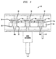
- FIG. 1 illustrates a chemical vapor deposition chamber 10 that can be used with the present invention.
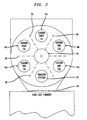
- the chamber 10 uses multi-station sequential deposition architecture, such as shown in FIG. 2, where five pedestals 12a-e are positioned in a circular arrangement to form five deposition stations 14a-e corresponding to the respective five pedestals.
- Each pedestal is formed as a platen for holding the semiconductor substrate or wafer indicated by a "W". Multiple wafers can be processed sequentially and receive a portion of their total deposition thickness at the separate and discrete deposition stations.
- An example of the type of chemical vapor deposition chamber that can be used in the present invention is a Novellus Altus Concept Two chemical vapor deposition chamber.
- Multi-station sequential deposition architecture is advantageous and it is possible to work with sub 0.25 micro technology. Wafers can be produced in excess of 110 wafers per hour (WPH) for thin films.
- the chamber includes a dual load lock and advanced wafer handling to increase system throughput.
- the chemical vapor deposition chamber 10 communicates with a load lock chamber 20 where wafers are introduced and received into and from the chamber 10 .
- the five deposition or process stations 14a-e are located within the chamber.
- a transfer station 22 allows transfer of wafers from the load lock chamber 20 to the chamber 10 and onto the platens .
- the chamber includes appropriate venting ports for gases.
- Each deposition station includes the pedestal 12a-e that is heated by a heater assembly shown at 24 , to provide heat to the platen semiconductor substrate.
- a gas dispersion head 30 also called a shower head in the industry, is positioned above each pedestal 12a-e and introduces the process gases over the wafer.
- Each pedestal, or platen supports the wafer.
- a pedestal base 32 supports the heater assembly 24 for heating the platen and supplying heat to the wafer.
- a pin lift mechanism is indicated by the dotted lines at 32 and formed to raise and lower wafers of the platens to process and work in conjunction with a wafer transport mechanism 34 that moves wafers to the pedestals in succession.
- the wafer transport mechanism could be formed as rotary arms 36 (FIG. 2) that lift and move the wafers into successive stations.
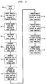
- the process begins (block 100) and the wafer enters the load lock chamber and is transferred onto the transfer pedestal or station (block 102).
- the semiconductor substrate or wafer is then transferred and received at the first deposition station onto the pedestal within the chamber (block 104).
- the semiconductor substrate is heated to a temperature between about 360°C and about 390°C and preferably about 375°C via the heater assembly and platen (block 106).
- the platen is set at a temperature about 15 degrees greater than the semiconductor wafer, i.e., substrate.
- An initiation gas is introduced for about ten seconds into the first deposition station onto the semiconductor substrate to form an amorphous, monolayer of silicon (block 108).
- This initiation gas comprises a silane (SiH 4 ) gas flow at a rate of about 40 to about 48 standard cubic centimeters per minute. Additionally, argon is continuously flowing at a rate of about 10,000 to about 12,000 standard cubic centimeters per minute.
- This sequence forms the first of seven layers. The first three layers occur at the first station 14a .
- This first, self-limiting, amorphous silicon layer is required to prevent long incubation times of chemically vapor deposited tungsten atop a titanium nitride (TiN) seed layer. This first layer also increases the subsequent tungsten film deposition rate and film uniformity and decreases subsequent film stress.
- a backside gas flow is introduced against a semiconductor substrate via heated platen for preventing backside deposition and front side edge deposit.
- This backside gas flow is maintained in subsequent processing.
- This backside gas flow is produced at all deposition stations 14a-e at all pedestals.
- the backside gas flow comprises an argon gas flow and a hydrogen gas flow, as known to those skilled in the art.
- the amount of argon gas flow flowing from the shower head can vary and can be used to control the rate of reaction.
- an argon gas flow at a rate of about 10,000 to about 12,000 standard cubic centimeters per minute has been found advantageous.
- the initiation gas is then terminated and a nucleation gas (block 110) introduced at the first deposition station to form a silane reduced tungsten layer.
- the nucleation gas comprises a silane gas flow of about 20 to about 30 standard cubic centimeters per minute, and a tungsten hexafluoride (WF 6 ) gas flow at a rate of about 300 to about 350 standard cubic centimeters per minute. This gas flow rate occurs for about ten seconds.
- WF 6 tungsten hexafluoride
- This gas flow rate occurs for about ten seconds.
- the use of silane during tungsten growth helps prevent the reaction between tungsten hexafluoride and titanium suicide.
- hydrogen also flows and is introduced at a rate of about 7,000 to about 8,500 standard cubic centimeters per minute.
- a third layer of seven layers is produced at the first deposition station 14a at pedestal one 12a and is the first layer of a hydrogen reduced bulk tungsten deposition layer (block 112).
- a 370 angstrom tungsten film is formed via a 20 second reduction of tungsten hexafluoride by flowing 300 to 350 standard cubic centimeters per minute of tungsten hexafluoride and hydrogen flowing at 7,000 to 8,500 standard cubic centimeters per minute.
- the wafer transport mechanism then moves the semiconductor substrate into respective deposition stations at pedestals 2-5 where layers 4-7 receive a bulk tungsten deposition (blocks 114, 116, 118 and 120).
- a bulk tungsten deposition blocks 114, 116, 118 and 120.
- a 560 angstrom film of bulk, hydrogen reduced, tungsten is deposited.
- Tungsten hexafluoride can be introduced at a flow rate of 300 to 350 standard cubic centimeters per minute, and hydrogen can flow at a rate of 7,000 to 8,500 standard cubic centimeters per minute, each for about 30 seconds. This 30 second rate is based on a 3,000 angstrom total tungsten film thickness. However, by linearly increasing or decreasing the bulk fill duration, it is possible to increase or decrease the tungsten thickness respectively, as will be known to those skilled in the art.
- the present invention is advantageous and provides a new and unobvious process that allows low temperature tungsten chemical vapor deposition in a multi-station sequential deposition system.
- it is now possible to reduce the propensity of defects caused by gas phase nucleation of tungsten and ensure robustness against WF 6 attack of Ti under layers (volcanos), and provide a low stress film at low temperature applications.
- Process Parameters Low temperature Standard Pedestal temperature 390°C 425°C Approx wafer temperature 375°C 410°C Front side argon 10,000-12,000 sccms 7,500 sccms Front side hydrogen 7,000-8,500 sccms 6,000 sccms Silane (initiation layer) 40-48 sccms 40 sccms Silane (seed layer) 20-30 sccms 40 sccms Tungsten hexafluoride 300-350 sccms 400 sccms Seed layer duration 10 seconds 8 seconds Total station deposition time 30 seconds 15 seconds 15 seconds
Landscapes
- Chemical & Material Sciences (AREA)
- General Chemical & Material Sciences (AREA)
- Chemical Kinetics & Catalysis (AREA)
- Engineering & Computer Science (AREA)
- Materials Engineering (AREA)
- Mechanical Engineering (AREA)
- Metallurgy (AREA)
- Organic Chemistry (AREA)
- Chemical Vapour Deposition (AREA)
- Electrodes Of Semiconductors (AREA)
Abstract
A method of depositing tungsten on a semiconductor
substrate is disclosed. The semiconductor substrate is
heated to between about 360°C and about 390°C and
preferably about 375°C. Initiation gases are introduced
into a first deposition station of a chemical vapor
deposition chamber to form an amorphous, monolayer of
silicon. Initiation gas comprises a silane gas flow at a
rate of about 40 to about 48 standard cubic centimeters per
minute. A nucleation gas flow rate formed of silane of
about 20 to about 30 standard cubic centimeters per minute
and a tungsten hexafluoride gas flow at a rate of about 300
to about 350 standard cubic standard centimeters per minute
is next introduced. A hydrogen reducing gas flow rate is
then introduced to form a layer of hydrogen reduced bulk
tungsten. This reduced gas flow comprises a hydrogen gas
flow at a rate of about 7,000 to about 8,500 standard cubic
centimeters per minute gas flow, and a tungsten hexafluoride
gas flow at a rate of about 300 to about 350 standard cubic
centimeters per minute. A bulk hydrogen reduced tungsten is
deposited at successive deposition stations.
Description
- This invention relates to the field of semiconductor manufacturing, and more particularly, this invention relates to the chemical vapor deposition of a tungsten film on a semiconductor substrate.
- Tungsten (W) films are deposited as a blanket layer using chemical vapor deposition (CVD) techniques during semiconductor manufacturing. The tungsten can be deposited through a chemical reduction of tungsten hexafluoride (WF6) using a hydrogen (H2) or silane (SiH4). Usually, the tungsten is deposited at temperatures ranging from 425°C to as high as 475°C, such as disclosed in the upper range of temperatures in U.S. Patent No. 5,795,824. In this prior art process, tungsten film is grown on a semiconductor substrate by positioning the semiconductor substrate within a chemical vapor deposition chamber having a number of different pedestals that are heated. Initiation gases, such as hydrogen and silane, are provided to initiate a growth at temperature ranges of 350 to 475°C, followed by nucleation with a gas flow that replaces the initiation gases, where tungsten film is formed at a rate in excess of approximately 100 NM/MIN on the surface. The hydrogen and silane gas flow occurs without argon gas at a first pedestal. The substrate is repositioned at a second deposition station or pedestal within the deposition chamber, followed by successive positioning at other pedestals.
- However, the current chemical vapor deposition tungsten processes are not adaptable for use with low-K dielectrics because the stability of dielectrics are compromised by the high tungsten deposition temperatures of 425 to 450°C. Thus, those processes that can be used with these higher temperatures are not adaptable for use with the low-K dielectrics requiring low temperature applications. It is difficult to fabricate any chemical vapor deposition tungsten plugs at temperatures around 375°C without extensive hardware modifications. More optimal gas species combinations, gas flows and gas flow sequences are required in the chemical vapor deposition chambers, such that a low resistivity, high reflectivity, and smaller grain size tungsten plug could be obtained at the lower temperatures compared to the prior art using the 425 to 450°C range. It would also be advantageous if there could be little hardware changes to existing chemical vapor deposition chambers. Instead, changes in the gas flow and gas species combinations and gas flow sequences are the better design choice.
- It is therefore an object of the present invention to provide a method for depositing tungsten at low temperatures of about 360 to about 390°C onto a semiconductor substrate having low-K dielectric materials.
- In accordance with the present invention, a method for depositing tungsten on a semiconductor substrate comprises the step of receiving the semiconductor substrate at a first deposition station within a chemical vapor deposition chamber having a plurality of discrete deposition stations. The semiconductor substrate is heated to a temperature between about 360 and about 390°C. Initiation gases are introduced into the first deposition station to form an amorphous, monolayer of silicon. The initiation gases comprise a silane (SiH4) gas that flows at a rate of about 40 to about 48 standard cubic centimeters per minute.
- Nucleation gases are introduced into the first deposition station to form a silane reduced tungsten layer. These nucleation gases comprise a silane gas flow of about 20 to about 30 standard cubic centimeters per minute and a tungsten hexafluoride (WF6) gas that flows at a rate of about 300 to about 350 standard cubic centimeters per minute.
- The hydrogen reducing gas flow is introduced to form a layer of hydrogen reduced bulk tungsten. The hydrogen reducing gas flow comprises a hydrogen gas flow of about 7,000 to about 8,500 standard cubic centimeters per minute gas flow and a tungsten hexafluoride gas flow of about 300 to about 350 standard cubic centimeters per minute. A bulk hydrogen reduced tungsten is then deposited at successive deposition stations.
- In another aspect of the present invention, a continuous flow of argon is introduced with the initiation and nucleation gas flows. Argon can be introduced in a continuous flow rate of about 10,000 to about 12,000 standard cubic centimeters per minute with the initiation and nucleation gas flows. In one aspect of the present invention, there are five deposition stations and argon is introduced at a continuous flow rate of about 10,000 to about 12,000 standard cubic centimeters per minute at all deposition stations. The total tungsten film thickness can be about 3,000 angstroms. Hydrogen gas flow can also be introduced at a gas flow of about 7,000 to about 8,500 standard cubic centimeters per minute with the initiation gas flow. In still another aspect of the present invention, the semiconductor substrate is heated to about 375°C.
- In still another aspect of the present invention, the process for depositing tungsten on a semiconductor substrate comprises the steps of receiving the semiconductor substrate at a first deposition station within a chemical vapor deposition chamber having a plurality of discrete deposition stations. The semiconductor substrate is heated to a temperature between about 360 and about 390°C. Initiation gases are introduced for about 10 seconds into the first deposition station to form an amorphous, monolayer of silicon. The initiation gases comprise a silane (SiH4) gas flow at a rate of about 40 to about 48 standard cubic centimeters per minute.
- Nucleation gases are then introduced for about 10 seconds into the first deposition station to form a silane reduced tungsten layer of about 400 angstroms. The nucleation gases comprise a silane gas flow of about 20 to about 30 standard cubic centimeters per minute and a tungsten hexafluoride (WF6) gas flow of about 300 to about 350 standard cubic centimeters per minute. A hydrogen reducing gas flow is introduced for about 20 seconds into the first deposition station to form a layer of hydrogen reduced bulk tungsten of about 370 angstroms. The hydrogen reducing gas flow comprises a hydrogen gas flow of about 7,000 to about 8,500 standard cubic centimeters per minute gas flow, and a tungsten hexafluoride gas flow rate of about 300 to about 350 standard cubic centimeters per minute.
- The semiconductor substrate is then received into successive deposition stations. At each successive deposition station, a gas flow is introduced for about 30 seconds to deposit a bulk, hydrogen reduced tungsten. The gas flow comprises a tungsten hexafluoride gas flowing at a rate of about 300 to about 350 standard cubic centimeters per minute and hydrogen flowing at a rate of about 7,000 to about 8,500 standard cubic centimeters per minute.
- In yet another aspect of the present invention, the semiconductor substrate is received on a heated platen at a first deposition station within a chemical vapor deposition chamber that has a plurality of discrete deposition stations with heated platens. The heated platens heat the semiconductor substrate to between about 360 to about 390°C, and preferably to about 375°C. At the same time, a backside gas flow is introduced against the semiconductor substrate and heated platen for preventing backside deposition and preventing front side edge deposition, e.g., edge exclusion, and maintaining the backside gas flow in subsequent processing.
- Other objects, features and advantages of the present invention will become apparent from the detailed description of the invention which follows, when considered in light of the accompanying drawings in which:
- FIG. 1 is a schematic, cross-sectional view of a multi-station, sequential chemical vapor deposition chamber that could be used for the present invention.
- FIG. 2 is a schematic, top plan view of the chemical vapor deposition chamber shown in FIG. 1.
- FIG. 3 is a flow chart illustrating the basic process of the present invention.
-
- The present invention is advantageous because it now permits the tungsten chemical vapor deposition of devices containing low-K dielectrics at low temperatures, such as around 360°C to about 390°C, and preferably around 375°C. The present invention is also advantageous because the low temperatures form grain sizes of tungsten that more readily fill the voids. Also, there are no major hardware modifications necessary for the practice of the present invention. These dielectrics have low thermal budgets and cannot be processed by those well known techniques and methods of prior art using higher temperature tungsten deposition temperatures of about 425°C to about 450°C. With the method of the present invention, chemical vapor deposited tungsten plugs can now be fabricated with a semiconductor material having a low-K dielectric material, such as those organic spin-on dielectrics known to those skilled in the art. These dielectrics can be integrated into the process of the present invention.
- As known to those skilled in the art, these low-K organic spin-on dielectrics and other similar dielectrics have a thermal stability problem above about 375°C to about 390°C. The resultant film structure of the present invention reduces the propensity to defects caused by gas phase nucleation of tungsten and ensures robustness against WF6 attack on Ti under layers (volcanos), and provides a low stress film. These factors provide a CVD-W deposition process that is necessary for a successful integration of a low-K dielectric material that loses stability if used in conjunction with prior art tungsten deposition processes.
- FIG. 1 illustrates a chemical
vapor deposition chamber 10 that can be used with the present invention. Thechamber 10 uses multi-station sequential deposition architecture, such as shown in FIG. 2, where fivepedestals 12a-e are positioned in a circular arrangement to form fivedeposition stations 14a-e corresponding to the respective five pedestals. Each pedestal is formed as a platen for holding the semiconductor substrate or wafer indicated by a "W". Multiple wafers can be processed sequentially and receive a portion of their total deposition thickness at the separate and discrete deposition stations. An example of the type of chemical vapor deposition chamber that can be used in the present invention is a Novellus Altus Concept Two chemical vapor deposition chamber. - As any wafers move to
successive stations 14a-e, a new wafer is introduced into the chemicalvapor deposition chamber 10, while a completed wafer is removed. Each wafer is exposed to the same processing environment at each station. This type of multi-station sequential deposition architecture allows reproducibility on a fine scale. Because the tungsten film is deposited slowly over the successive steps at eitherstations 14a-e, this type of architecture averages out random process variations and yields uniform films. If any flaws are produced at one pedestal, e.g., where a partial deposition occurs only, the next pedestal deposition will even out the deposition flows and correct the defects. - Multi-station sequential deposition architecture is advantageous and it is possible to work with sub 0.25 micro technology. Wafers can be produced in excess of 110 wafers per hour (WPH) for thin films. The chamber includes a dual load lock and advanced wafer handling to increase system throughput.
- As shown in the schematic cross-sectional view of FIG. 1 and the top plan view of FIG. 2, the chemical
vapor deposition chamber 10 communicates with aload lock chamber 20 where wafers are introduced and received into and from thechamber 10. The five deposition orprocess stations 14a-e are located within the chamber. Atransfer station 22 allows transfer of wafers from theload lock chamber 20 to thechamber 10 and onto the platens . Naturally, the chamber includes appropriate venting ports for gases. - Each deposition station includes the
pedestal 12a-e that is heated by a heater assembly shown at 24, to provide heat to the platen semiconductor substrate. Agas dispersion head 30, also called a shower head in the industry, is positioned above eachpedestal 12a-e and introduces the process gases over the wafer. Each pedestal, or platen, supports the wafer. Apedestal base 32 supports theheater assembly 24 for heating the platen and supplying heat to the wafer. A pin lift mechanism is indicated by the dotted lines at 32 and formed to raise and lower wafers of the platens to process and work in conjunction with awafer transport mechanism 34 that moves wafers to the pedestals in succession. The wafer transport mechanism could be formed as rotary arms 36 (FIG. 2) that lift and move the wafers into successive stations. - An example of various types of chamber designs that could be used with the present invention are those types of designs shown in U.S. Patent Nos. 5,374,594, 5,679,405, and 5,882,417, the disclosures which are hereby incorporated by reference in their entirety. During gas flow processing, a backside gas flow is introduced through backside gas
flow discharge port 40 and throughchannels 40a onto the backside of the wafer to prevent backside deposition and front side edge deposit, as known to those skilled in the art. - Referring now to the flow chart of FIG. 3, the basic method of the present invention is illustrated. For purposes of clarity, the term wafer and semiconductor substrate will be used interchangeably. In accordance with the process and method of the present invention, the process begins (block 100) and the wafer enters the load lock chamber and is transferred onto the transfer pedestal or station (block 102). The semiconductor substrate or wafer is then transferred and received at the first deposition station onto the pedestal within the chamber (block 104). The semiconductor substrate is heated to a temperature between about 360°C and about 390°C and preferably about 375°C via the heater assembly and platen (block 106). The platen is set at a temperature about 15 degrees greater than the semiconductor wafer, i.e., substrate. An initiation gas is introduced for about ten seconds into the first deposition station onto the semiconductor substrate to form an amorphous, monolayer of silicon (block 108). This initiation gas comprises a silane (SiH4) gas flow at a rate of about 40 to about 48 standard cubic centimeters per minute. Additionally, argon is continuously flowing at a rate of about 10,000 to about 12,000 standard cubic centimeters per minute. This sequence forms the first of seven layers. The first three layers occur at the
first station 14a. This first, self-limiting, amorphous silicon layer is required to prevent long incubation times of chemically vapor deposited tungsten atop a titanium nitride (TiN) seed layer. This first layer also increases the subsequent tungsten film deposition rate and film uniformity and decreases subsequent film stress. - At the same time, a backside gas flow is introduced against a semiconductor substrate via heated platen for preventing backside deposition and front side edge deposit. This backside gas flow is maintained in subsequent processing. This backside gas flow is produced at all
deposition stations 14a-e at all pedestals. The backside gas flow comprises an argon gas flow and a hydrogen gas flow, as known to those skilled in the art. Naturally, the amount of argon gas flow flowing from the shower head can vary and can be used to control the rate of reaction. However, for the present invention, an argon gas flow at a rate of about 10,000 to about 12,000 standard cubic centimeters per minute has been found advantageous. - The initiation gas is then terminated and a nucleation gas (block 110) introduced at the first deposition station to form a silane reduced tungsten layer. The nucleation gas comprises a silane gas flow of about 20 to about 30 standard cubic centimeters per minute, and a tungsten hexafluoride (WF6) gas flow at a rate of about 300 to about 350 standard cubic centimeters per minute. This gas flow rate occurs for about ten seconds. The use of silane during tungsten growth helps prevent the reaction between tungsten hexafluoride and titanium suicide. During this step, hydrogen also flows and is introduced at a rate of about 7,000 to about 8,500 standard cubic centimeters per minute.
- Because this reaction between silane and tungsten hexafluoride occurs rapidly, it has been found necessary to move to a slower reaction of hydrogen reduction of tungsten hexafluoride. A third layer of seven layers is produced at the
first deposition station 14a at pedestal one 12a and is the first layer of a hydrogen reduced bulk tungsten deposition layer (block 112). A 370 angstrom tungsten film is formed via a 20 second reduction of tungsten hexafluoride by flowing 300 to 350 standard cubic centimeters per minute of tungsten hexafluoride and hydrogen flowing at 7,000 to 8,500 standard cubic centimeters per minute. - Once this third layer is completed, the wafer transport mechanism then moves the semiconductor substrate into respective deposition stations at pedestals 2-5 where layers 4-7 receive a bulk tungsten deposition (
blocks pedestal chamber 10. - The present invention is advantageous and provides a new and unobvious process that allows low temperature tungsten chemical vapor deposition in a multi-station sequential deposition system. Thus, it is now possible to reduce the propensity of defects caused by gas phase nucleation of tungsten and ensure robustness against WF6 attack of Ti under layers (volcanos), and provide a low stress film at low temperature applications.
- The following table shows a some of the operating parameters of the low temperature process versus a standard prior art process as could be used with the present invention.
Process Parameters Low temperature Standard Pedestal temperature 390°C 425°C Approx wafer temperature 375°C 410°C Front side argon 10,000-12,000 sccms 7,500 sccms Front side hydrogen 7,000-8,500 sccms 6,000 sccms Silane (initiation layer) 40-48 sccms 40 sccms Silane (seed layer) 20-30 sccms 40 sccms Tungsten hexafluoride 300-350 sccms 400 sccms Seed layer duration 10 seconds 8 seconds Total station deposition time 30 seconds 15 seconds
Claims (14)
- A method for depositing tungsten on a semiconductor substrate comprising the steps of:receiving the semiconductor substrate at a first deposition station within a chemical vapor deposition chamber having a plurality of discrete deposition stations;heating the semiconductor substrate to a temperature between about 360 and about 390 degrees centigrade;introducing initiation gases into the first deposition station to form an amorphous, monolayer of silicon, wherein the initiation gases comprise a silane (SiH4) gas flow of about 40 to about 48 standard cubic centimeters per minute;introducing nucleation gases into the first deposition station to form a silane reduced tungsten layer, wherein the nucleation gases comprise a silane gas flow of about 20 to about 30 standard cubic centimeters per minute and a tungsten hexafluoride (WF6) gas flow of about 300 to about 350 standard cubic centimeters per minute;introducing a hydrogen reducing gas flow to form a layer of hydrogen reduced bulk tungsten, wherein the hydrogen reducing gas flow comprises a hydrogen gas flow of about 7,000 to about 8,500 standard cubic centimeters per minute and a tungsten hexafluoride gas flow of about 300 to about 350 standard cubic centimeters per minute; anddepositing at successive deposition stations a bulk, hydrogen reduced tungsten.
- A method for depositing tungsten on a semiconductor substrate comprising the steps of:receiving the semiconductor substrate at a first deposition station within a chemical vapor deposition chamber having a plurality of discrete deposition stations;heating the semiconductor substrate to a temperature between about 360 and about 390 degrees centigrade;introducing initiation gases for about 10 seconds into the first deposition station to form an amorphous, monolayer of silicon, wherein the initiation gases comprise a silane (SiH4) gas flow of about 40 to about 48 standard cubic centimeters per minute;introducing nucleation gases for about 10 seconds into the first deposition station to form a silane reduced tungsten layer of about 400 angstroms thickness, wherein the nucleation gases comprise a silane gas flow of about 20 to about 30 standard cubic centimeters per minute and a tungsten hexafluoride (WF6) gas flow of about 300 to about 350 standard cubic centimeters per minute;introducing a hydrogen reducing gas flow for about 20 seconds into the first deposition station to form a layer of hydrogen reduced bulk tungsten of about 370 angstroms, wherein the hydrogen reducing gas flow comprises a hydrogen gas flow of about 7,000 to about 8,500 standard cubic centimeters per minute and a tungsten hexafluoride gas flow of about 300 to about 350 standard cubic centimeters per minute;receiving the semiconductor substrate into successive deposition stations; andintroducing at each successive deposition station a gas flow for about 30 seconds to deposit a bulk, hydrogen reduced tungsten, said gas flow comprising tungsten hexafluoride flow of about 300 to about 350 standard cubic centimeters per minute and hydrogen flow of about 7,000 to about 8,500 standard cubic centimeters per minute.
- A method according to claim 2, wherein each deposition station comprises a heated platen on which the semiconductor substrate is positioned.
- A method according to claim 3, and further comprising the step of introducing a backside gas flow against the semiconductor substrate and heated platen for preventing backside deposition and front side edge deposit.
- A method for depositing tungsten on a semiconductor substrate comprising the steps of:receiving the semiconductor substrate on a heated platen at a first deposition station within a chemical vapor deposition chamber having a plurality of discrete deposition stations, each deposition chamber having a heated platen that heats the semiconductor substrate to between about 360 and about 390 degrees centigrade;introducing initiation gases into the first deposition station to form an amorphous, monolayer of silicon, wherein the initiation gases comprise a silane (SiH4) gas flow of about 40 to about 48 standard cubic centimeters per minute while also introducing a backside gas flow against the semiconductor substrate and heated platen for preventing backside deposition and front side edge deposit and maintaining the backside gas flow in subsequent processing;introducing nucleation gases into the first deposition station to form a silane reduced tungsten layer, wherein the nucleation gases comprise a silane gas flow of about 20 to about 30 standard cubic centimeters per minute and a tungsten hexafluoride (WF6) gas flow of about 300 to about 350 standard cubic centimeters per minute;introducing a hydrogen reducing gas flow to form a layer of hydrogen reduced bulk tungsten, wherein the hydrogen reducing gas flow, comprises a hydrogen gas flow of about 7,000 to about 8,500 standard cubic centimeters per minute and a tungsten hexafluoride gas flow of about 300 to about 350 standard cubic centimeters per minute; anddepositing at successive deposition stations a bulk, hydrogen reduced tungsten.
- A method according to any of the preceding claims, and further comprising the step of introducing a continuous flow of argon with the initiation and nucleation gas flows.
- A method according to claim 6, and further comprising the step of introducing argon in a continuous flow rate of about 10,000 to about 12,000 standard cubic centimeters per minute with the initiation and nucleation gas flows.
- A method according to claim 6, and further comprising the step of introducing argon in a continuous flow rate of about 10,000 to about 12,000 standard cubic centimeters per minute at all deposition stations.
- A method according to any of the preceding claims, wherein said deposition chamber comprises five deposition stations.
- A method according to any of the preceding claims, and further comprising the step of introducing a hydrogen gas flow of about 7,000 to about 8,500 standard cubic centimeters per minute with the nucleation gas flow.
- A method according to claim 4 or claim 5, wherein the backside gas flow comprises an argon and hydrogen gas flow.
- A method according to claim 9, wherein each semiconductor substrate is heated to about 375 degrees centigrade.
- A method according to any of the preceding claims, and further comprising the step of forming a 3,000 angstrom total tungsten film thickness.
- A method according to claim 13 wherein said total tungsten film thickness is formed in seven layers.
Applications Claiming Priority (4)
| Application Number | Priority Date | Filing Date | Title |
|---|---|---|---|
| US13556499P | 1999-05-24 | 1999-05-24 | |
| US135564P | 1999-05-24 | ||
| US09/517,965 US6294468B1 (en) | 1999-05-24 | 2000-03-03 | Method of chemical vapor depositing tungsten films |
| US517965 | 2000-03-03 |
Publications (1)
| Publication Number | Publication Date |
|---|---|
| EP1055746A1 true EP1055746A1 (en) | 2000-11-29 |
Family
ID=26833447
Family Applications (1)
| Application Number | Title | Priority Date | Filing Date |
|---|---|---|---|
| EP00304055A Withdrawn EP1055746A1 (en) | 1999-05-24 | 2000-05-15 | Method of chemical vapor depositing tungsten films |
Country Status (4)
| Country | Link |
|---|---|
| US (1) | US6294468B1 (en) |
| EP (1) | EP1055746A1 (en) |
| JP (1) | JP2001007048A (en) |
| KR (1) | KR20000077359A (en) |
Cited By (13)
| Publication number | Priority date | Publication date | Assignee | Title |
|---|---|---|---|---|
| KR100379108B1 (en) * | 2001-03-30 | 2003-04-07 | 삼성전자주식회사 | CONTROL OF ABNORMAL GROWTH IN DICHLORO SILANE(DCS) BASED CVD POLYCIDE WSix FILMS |
| US8835317B2 (en) | 2009-08-04 | 2014-09-16 | Novellus Systems, Inc. | Depositing tungsten into high aspect ratio features |
| US9034768B2 (en) | 2010-07-09 | 2015-05-19 | Novellus Systems, Inc. | Depositing tungsten into high aspect ratio features |
| US9082826B2 (en) | 2013-05-24 | 2015-07-14 | Lam Research Corporation | Methods and apparatuses for void-free tungsten fill in three-dimensional semiconductor features |
| US9240347B2 (en) | 2012-03-27 | 2016-01-19 | Novellus Systems, Inc. | Tungsten feature fill |
| US9548228B2 (en) | 2009-08-04 | 2017-01-17 | Lam Research Corporation | Void free tungsten fill in different sized features |
| US9589835B2 (en) | 2008-12-10 | 2017-03-07 | Novellus Systems, Inc. | Method for forming tungsten film having low resistivity, low roughness and high reflectivity |
| US9972504B2 (en) | 2015-08-07 | 2018-05-15 | Lam Research Corporation | Atomic layer etching of tungsten for enhanced tungsten deposition fill |
| CN108039497A (en) * | 2017-12-20 | 2018-05-15 | 北京理工大学 | One kind has the preparation method of the tungsten coating of high { 110 } crystal face share |
| US9978610B2 (en) | 2015-08-21 | 2018-05-22 | Lam Research Corporation | Pulsing RF power in etch process to enhance tungsten gapfill performance |
| US10256142B2 (en) | 2009-08-04 | 2019-04-09 | Novellus Systems, Inc. | Tungsten feature fill with nucleation inhibition |
| US10566211B2 (en) | 2016-08-30 | 2020-02-18 | Lam Research Corporation | Continuous and pulsed RF plasma for etching metals |
| US12444651B2 (en) | 2009-08-04 | 2025-10-14 | Novellus Systems, Inc. | Tungsten feature fill with nucleation inhibition |
Families Citing this family (39)
| Publication number | Priority date | Publication date | Assignee | Title |
|---|---|---|---|---|
| KR100326253B1 (en) * | 1999-12-28 | 2002-03-08 | 박종섭 | Method for forming capacitor in semiconductor device |
| US7262125B2 (en) * | 2001-05-22 | 2007-08-28 | Novellus Systems, Inc. | Method of forming low-resistivity tungsten interconnects |
| US7955972B2 (en) * | 2001-05-22 | 2011-06-07 | Novellus Systems, Inc. | Methods for growing low-resistivity tungsten for high aspect ratio and small features |
| US7141494B2 (en) * | 2001-05-22 | 2006-11-28 | Novellus Systems, Inc. | Method for reducing tungsten film roughness and improving step coverage |
| US9076843B2 (en) | 2001-05-22 | 2015-07-07 | Novellus Systems, Inc. | Method for producing ultra-thin tungsten layers with improved step coverage |
| US7589017B2 (en) * | 2001-05-22 | 2009-09-15 | Novellus Systems, Inc. | Methods for growing low-resistivity tungsten film |
| US7005372B2 (en) * | 2003-01-21 | 2006-02-28 | Novellus Systems, Inc. | Deposition of tungsten nitride |
| US6635965B1 (en) * | 2001-05-22 | 2003-10-21 | Novellus Systems, Inc. | Method for producing ultra-thin tungsten layers with improved step coverage |
| US6844258B1 (en) | 2003-05-09 | 2005-01-18 | Novellus Systems, Inc. | Selective refractory metal and nitride capping |
| US7754604B2 (en) * | 2003-08-26 | 2010-07-13 | Novellus Systems, Inc. | Reducing silicon attack and improving resistivity of tungsten nitride film |
| KR100890047B1 (en) * | 2007-06-28 | 2009-03-25 | 주식회사 하이닉스반도체 | Wiring Formation Method of Semiconductor Device |
| US7655567B1 (en) | 2007-07-24 | 2010-02-02 | Novellus Systems, Inc. | Methods for improving uniformity and resistivity of thin tungsten films |
| US8049178B2 (en) * | 2007-08-30 | 2011-11-01 | Washington State University Research Foundation | Semiconductive materials and associated uses thereof |
| US7772114B2 (en) | 2007-12-05 | 2010-08-10 | Novellus Systems, Inc. | Method for improving uniformity and adhesion of low resistivity tungsten film |
| US8053365B2 (en) | 2007-12-21 | 2011-11-08 | Novellus Systems, Inc. | Methods for forming all tungsten contacts and lines |
| US8062977B1 (en) | 2008-01-31 | 2011-11-22 | Novellus Systems, Inc. | Ternary tungsten-containing resistive thin films |
| US8058170B2 (en) * | 2008-06-12 | 2011-11-15 | Novellus Systems, Inc. | Method for depositing thin tungsten film with low resistivity and robust micro-adhesion characteristics |
| US8551885B2 (en) * | 2008-08-29 | 2013-10-08 | Novellus Systems, Inc. | Method for reducing tungsten roughness and improving reflectivity |
| US9159571B2 (en) | 2009-04-16 | 2015-10-13 | Lam Research Corporation | Tungsten deposition process using germanium-containing reducing agent |
| US8623733B2 (en) * | 2009-04-16 | 2014-01-07 | Novellus Systems, Inc. | Methods for depositing ultra thin low resistivity tungsten film for small critical dimension contacts and interconnects |
| US8119527B1 (en) * | 2009-08-04 | 2012-02-21 | Novellus Systems, Inc. | Depositing tungsten into high aspect ratio features |
| US8207062B2 (en) * | 2009-09-09 | 2012-06-26 | Novellus Systems, Inc. | Method for improving adhesion of low resistivity tungsten/tungsten nitride layers |
| US8709948B2 (en) | 2010-03-12 | 2014-04-29 | Novellus Systems, Inc. | Tungsten barrier and seed for copper filled TSV |
| US9034760B2 (en) | 2012-06-29 | 2015-05-19 | Novellus Systems, Inc. | Methods of forming tensile tungsten films and compressive tungsten films |
| US8975184B2 (en) | 2012-07-27 | 2015-03-10 | Novellus Systems, Inc. | Methods of improving tungsten contact resistance in small critical dimension features |
| US8853080B2 (en) | 2012-09-09 | 2014-10-07 | Novellus Systems, Inc. | Method for depositing tungsten film with low roughness and low resistivity |
| US9153486B2 (en) | 2013-04-12 | 2015-10-06 | Lam Research Corporation | CVD based metal/semiconductor OHMIC contact for high volume manufacturing applications |
| US9589808B2 (en) | 2013-12-19 | 2017-03-07 | Lam Research Corporation | Method for depositing extremely low resistivity tungsten |
| US9997405B2 (en) | 2014-09-30 | 2018-06-12 | Lam Research Corporation | Feature fill with nucleation inhibition |
| US9953984B2 (en) | 2015-02-11 | 2018-04-24 | Lam Research Corporation | Tungsten for wordline applications |
| US9978605B2 (en) | 2015-05-27 | 2018-05-22 | Lam Research Corporation | Method of forming low resistivity fluorine free tungsten film without nucleation |
| US9613818B2 (en) | 2015-05-27 | 2017-04-04 | Lam Research Corporation | Deposition of low fluorine tungsten by sequential CVD process |
| US9754824B2 (en) | 2015-05-27 | 2017-09-05 | Lam Research Corporation | Tungsten films having low fluorine content |
| KR20250073535A (en) | 2017-08-14 | 2025-05-27 | 램 리써치 코포레이션 | Metal fill process for three-dimensional vertical nand wordline |
| WO2019213604A1 (en) | 2018-05-03 | 2019-11-07 | Lam Research Corporation | Method of depositing tungsten and other metals in 3d nand structures |
| JP7649741B2 (en) | 2018-12-14 | 2025-03-21 | ラム リサーチ コーポレーション | Atomic Layer Deposition on 3D NAND Structures |
| US12002679B2 (en) | 2019-04-11 | 2024-06-04 | Lam Research Corporation | High step coverage tungsten deposition |
| JP2022533834A (en) | 2019-05-22 | 2022-07-26 | ラム リサーチ コーポレーション | Tungsten deposition without nucleation |
| US12077858B2 (en) | 2019-08-12 | 2024-09-03 | Lam Research Corporation | Tungsten deposition |
Citations (6)
| Publication number | Priority date | Publication date | Assignee | Title |
|---|---|---|---|---|
| JPH01160011A (en) * | 1987-12-17 | 1989-06-22 | Fujitsu Ltd | Manufacture of semiconductor device |
| EP0372861A2 (en) * | 1988-12-09 | 1990-06-13 | AT&T Corp. | Semiconductor integrated-circuit device metallization |
| EP0651436A1 (en) * | 1993-10-22 | 1995-05-03 | AT&T Corp. | Tungsten conductors formation process for semiconductor integrated circuits |
| US5489552A (en) * | 1994-12-30 | 1996-02-06 | At&T Corp. | Multiple layer tungsten deposition process |
| EP0857795A1 (en) * | 1997-02-06 | 1998-08-12 | Siemens Aktiengesellschaft | Method for coating a surface |
| US5840366A (en) * | 1994-09-09 | 1998-11-24 | Anelva Corporation | Method of forming thin film |
Family Cites Families (6)
| Publication number | Priority date | Publication date | Assignee | Title |
|---|---|---|---|---|
| US5230741A (en) | 1990-07-16 | 1993-07-27 | Novellus Systems, Inc. | Gas-based backside protection during substrate processing |
| US5133284A (en) | 1990-07-16 | 1992-07-28 | National Semiconductor Corp. | Gas-based backside protection during substrate processing |
| US5843233A (en) | 1990-07-16 | 1998-12-01 | Novellus Systems, Inc. | Exclusion guard and gas-based substrate protection for chemical vapor deposition apparatus |
| US5470768A (en) * | 1992-08-07 | 1995-11-28 | Fujitsu Limited | Method for fabricating a thin-film transistor |
| JPH09232423A (en) * | 1996-02-21 | 1997-09-05 | Nec Corp | Semiconductor device and manufacturing method thereof |
| US5795824A (en) | 1997-08-28 | 1998-08-18 | Novellus Systems, Inc. | Method for nucleation of CVD tungsten films |
-
2000
- 2000-03-03 US US09/517,965 patent/US6294468B1/en not_active Expired - Lifetime
- 2000-05-15 EP EP00304055A patent/EP1055746A1/en not_active Withdrawn
- 2000-05-20 KR KR1020000027214A patent/KR20000077359A/en not_active Withdrawn
- 2000-05-23 JP JP2000151544A patent/JP2001007048A/en active Pending
Patent Citations (6)
| Publication number | Priority date | Publication date | Assignee | Title |
|---|---|---|---|---|
| JPH01160011A (en) * | 1987-12-17 | 1989-06-22 | Fujitsu Ltd | Manufacture of semiconductor device |
| EP0372861A2 (en) * | 1988-12-09 | 1990-06-13 | AT&T Corp. | Semiconductor integrated-circuit device metallization |
| EP0651436A1 (en) * | 1993-10-22 | 1995-05-03 | AT&T Corp. | Tungsten conductors formation process for semiconductor integrated circuits |
| US5840366A (en) * | 1994-09-09 | 1998-11-24 | Anelva Corporation | Method of forming thin film |
| US5489552A (en) * | 1994-12-30 | 1996-02-06 | At&T Corp. | Multiple layer tungsten deposition process |
| EP0857795A1 (en) * | 1997-02-06 | 1998-08-12 | Siemens Aktiengesellschaft | Method for coating a surface |
Non-Patent Citations (1)
| Title |
|---|
| PATENT ABSTRACTS OF JAPAN vol. 013, no. 429 (E - 823) 25 September 1989 (1989-09-25) * |
Cited By (18)
| Publication number | Priority date | Publication date | Assignee | Title |
|---|---|---|---|---|
| KR100379108B1 (en) * | 2001-03-30 | 2003-04-07 | 삼성전자주식회사 | CONTROL OF ABNORMAL GROWTH IN DICHLORO SILANE(DCS) BASED CVD POLYCIDE WSix FILMS |
| US9589835B2 (en) | 2008-12-10 | 2017-03-07 | Novellus Systems, Inc. | Method for forming tungsten film having low resistivity, low roughness and high reflectivity |
| US10103058B2 (en) | 2009-08-04 | 2018-10-16 | Novellus Systems, Inc. | Tungsten feature fill |
| US8835317B2 (en) | 2009-08-04 | 2014-09-16 | Novellus Systems, Inc. | Depositing tungsten into high aspect ratio features |
| US12444651B2 (en) | 2009-08-04 | 2025-10-14 | Novellus Systems, Inc. | Tungsten feature fill with nucleation inhibition |
| US9548228B2 (en) | 2009-08-04 | 2017-01-17 | Lam Research Corporation | Void free tungsten fill in different sized features |
| US9653353B2 (en) | 2009-08-04 | 2017-05-16 | Novellus Systems, Inc. | Tungsten feature fill |
| US10256142B2 (en) | 2009-08-04 | 2019-04-09 | Novellus Systems, Inc. | Tungsten feature fill with nucleation inhibition |
| US9034768B2 (en) | 2010-07-09 | 2015-05-19 | Novellus Systems, Inc. | Depositing tungsten into high aspect ratio features |
| US9240347B2 (en) | 2012-03-27 | 2016-01-19 | Novellus Systems, Inc. | Tungsten feature fill |
| US9082826B2 (en) | 2013-05-24 | 2015-07-14 | Lam Research Corporation | Methods and apparatuses for void-free tungsten fill in three-dimensional semiconductor features |
| US9972504B2 (en) | 2015-08-07 | 2018-05-15 | Lam Research Corporation | Atomic layer etching of tungsten for enhanced tungsten deposition fill |
| US11069535B2 (en) | 2015-08-07 | 2021-07-20 | Lam Research Corporation | Atomic layer etch of tungsten for enhanced tungsten deposition fill |
| US9978610B2 (en) | 2015-08-21 | 2018-05-22 | Lam Research Corporation | Pulsing RF power in etch process to enhance tungsten gapfill performance |
| US10395944B2 (en) | 2015-08-21 | 2019-08-27 | Lam Research Corporation | Pulsing RF power in etch process to enhance tungsten gapfill performance |
| US10566211B2 (en) | 2016-08-30 | 2020-02-18 | Lam Research Corporation | Continuous and pulsed RF plasma for etching metals |
| CN108039497A (en) * | 2017-12-20 | 2018-05-15 | 北京理工大学 | One kind has the preparation method of the tungsten coating of high { 110 } crystal face share |
| CN108039497B (en) * | 2017-12-20 | 2020-11-06 | 北京理工大学 | Preparation method of tungsten coating with high {110} crystal face share |
Also Published As
| Publication number | Publication date |
|---|---|
| KR20000077359A (en) | 2000-12-26 |
| US6294468B1 (en) | 2001-09-25 |
| JP2001007048A (en) | 2001-01-12 |
Similar Documents
| Publication | Publication Date | Title |
|---|---|---|
| US6294468B1 (en) | Method of chemical vapor depositing tungsten films | |
| US9583385B2 (en) | Method for producing ultra-thin tungsten layers with improved step coverage | |
| US6635965B1 (en) | Method for producing ultra-thin tungsten layers with improved step coverage | |
| US11594415B2 (en) | PECVD tungsten containing hardmask films and methods of making | |
| US6548402B2 (en) | Method of depositing a thick titanium nitride film | |
| EP0644951B1 (en) | Method of nucleating tungsten on titanium nitride by cvd without silane | |
| US6797340B2 (en) | Method for depositing refractory metal layers employing sequential deposition techniques | |
| US20190259652A1 (en) | Oxidative Volumetric Expansion Of Metals And Metal Containing Compounds | |
| US7405158B2 (en) | Methods for depositing tungsten layers employing atomic layer deposition techniques | |
| US6555183B2 (en) | Plasma treatment of a titanium nitride film formed by chemical vapor deposition | |
| US5240505A (en) | Method of an apparatus for forming thin film for semiconductor device | |
| US7655567B1 (en) | Methods for improving uniformity and resistivity of thin tungsten films | |
| EP0134645B1 (en) | Method of forming thin film | |
| US20030127043A1 (en) | Pulsed nucleation deposition of tungsten layers | |
| US20080226822A1 (en) | Precoat film forming method, idling method of film forming device, loading table structure, film forming device and film forming method | |
| JP2008523640A (en) | Process sequence of deep trench doped silicon filling | |
| JP4126165B2 (en) | Multi-deposition SACVD reactor | |
| US6436820B1 (en) | Method for the CVD deposition of a low residual halogen content multi-layered titanium nitride film having a combined thickness greater than 1000 Å | |
| JP3381774B2 (en) | Method of forming CVD-Ti film | |
| US10854511B2 (en) | Methods of lowering wordline resistance | |
| US5849629A (en) | Method of forming a low stress polycide conductors on a semiconductor chip | |
| US6387445B1 (en) | Tungsten layer forming method and laminate structure of tungsten layer | |
| US6180513B1 (en) | Apparatus and method for manufacturing a semiconductor device having a multi-wiring layer structure | |
| JPH06291042A (en) | Selective vapor growth method and device |
Legal Events
| Date | Code | Title | Description |
|---|---|---|---|
| PUAI | Public reference made under article 153(3) epc to a published international application that has entered the european phase |
Free format text: ORIGINAL CODE: 0009012 |
|
| AK | Designated contracting states |
Kind code of ref document: A1 Designated state(s): DE FR GB IT NL |
|
| AX | Request for extension of the european patent |
Free format text: AL;LT;LV;MK;RO;SI |
|
| 17P | Request for examination filed |
Effective date: 20010529 |
|
| AKX | Designation fees paid |
Free format text: DE FR GB IT NL |
|
| STAA | Information on the status of an ep patent application or granted ep patent |
Free format text: STATUS: THE APPLICATION IS DEEMED TO BE WITHDRAWN |
|
| 18D | Application deemed to be withdrawn |
Effective date: 20021203 |