EP1054406A2 - Ferroelectric non-volatile memory device - Google Patents
Ferroelectric non-volatile memory device Download PDFInfo
- Publication number
- EP1054406A2 EP1054406A2 EP00109433A EP00109433A EP1054406A2 EP 1054406 A2 EP1054406 A2 EP 1054406A2 EP 00109433 A EP00109433 A EP 00109433A EP 00109433 A EP00109433 A EP 00109433A EP 1054406 A2 EP1054406 A2 EP 1054406A2
- Authority
- EP
- European Patent Office
- Prior art keywords
- transistor
- gate electrode
- memory device
- capacitors
- ferroelectric
- Prior art date
- Legal status (The legal status is an assumption and is not a legal conclusion. Google has not performed a legal analysis and makes no representation as to the accuracy of the status listed.)
- Granted
Links
Images


Classifications
-
- G—PHYSICS
- G11—INFORMATION STORAGE
- G11C—STATIC STORES
- G11C11/00—Digital stores characterised by the use of particular electric or magnetic storage elements; Storage elements therefor
- G11C11/21—Digital stores characterised by the use of particular electric or magnetic storage elements; Storage elements therefor using electric elements
- G11C11/22—Digital stores characterised by the use of particular electric or magnetic storage elements; Storage elements therefor using electric elements using ferroelectric elements
- G11C11/221—Digital stores characterised by the use of particular electric or magnetic storage elements; Storage elements therefor using electric elements using ferroelectric elements using ferroelectric capacitors
-
- G—PHYSICS
- G11—INFORMATION STORAGE
- G11C—STATIC STORES
- G11C11/00—Digital stores characterised by the use of particular electric or magnetic storage elements; Storage elements therefor
- G11C11/21—Digital stores characterised by the use of particular electric or magnetic storage elements; Storage elements therefor using electric elements
- G11C11/22—Digital stores characterised by the use of particular electric or magnetic storage elements; Storage elements therefor using electric elements using ferroelectric elements
- G11C11/225—Auxiliary circuits
- G11C11/2273—Reading or sensing circuits or methods
-
- G—PHYSICS
- G11—INFORMATION STORAGE
- G11C—STATIC STORES
- G11C11/00—Digital stores characterised by the use of particular electric or magnetic storage elements; Storage elements therefor
- G11C11/21—Digital stores characterised by the use of particular electric or magnetic storage elements; Storage elements therefor using electric elements
- G11C11/22—Digital stores characterised by the use of particular electric or magnetic storage elements; Storage elements therefor using electric elements using ferroelectric elements
- G11C11/225—Auxiliary circuits
- G11C11/2275—Writing or programming circuits or methods
-
- H—ELECTRICITY
- H10—SEMICONDUCTOR DEVICES; ELECTRIC SOLID-STATE DEVICES NOT OTHERWISE PROVIDED FOR
- H10B—ELECTRONIC MEMORY DEVICES
- H10B53/00—Ferroelectric RAM [FeRAM] devices comprising ferroelectric memory capacitors
-
- G—PHYSICS
- G11—INFORMATION STORAGE
- G11C—STATIC STORES
- G11C11/00—Digital stores characterised by the use of particular electric or magnetic storage elements; Storage elements therefor
- G11C11/21—Digital stores characterised by the use of particular electric or magnetic storage elements; Storage elements therefor using electric elements
- G11C11/22—Digital stores characterised by the use of particular electric or magnetic storage elements; Storage elements therefor using electric elements using ferroelectric elements
- G11C11/223—Digital stores characterised by the use of particular electric or magnetic storage elements; Storage elements therefor using electric elements using ferroelectric elements using MOS with ferroelectric gate insulating film
Abstract
Description
- The present invention relates to a ferroelectric non-volatile memory device and, more particularly, to a ferroelectric non-volatile memory device having a ferroelectric capacitor connected to the gate of a MOS (Metal Oxide Semiconductor) or MIS (Metal Insulator Semiconductor) field effect transistor.
- Forming a junction between a semiconductor and a ferroelectric is expected to create, depending on the polarization direction of the ferroelectric, a state in which electrons are induced to the semiconductor surface, or a state in which holes are induced. Attempts have already been made to manufacture non-volatile memory devices which hold memory contents even after power-off operation by using a ferroelectric for the gate insulator film of a MOS field effect transistor and making the two states correspond to "0" and "1". However, no practical devices have been realized yet. Devices with this structure are difficult to manufacture because of the following main reason. If a semiconductor and ferroelectric are joined to each other, an interface state is formed to capture electrons and holes. This stops flowing a necessary current through the source-drain path of a field effect transistor.
- To solve this problem, an MFIS (M: Metal or Conductor, F: Ferroelectric, I: Insulator, S: Semiconductor) structure and an MFMIS structure are proposed. In the MFIS structure, a dielectric (paraelectric) film such as a silicon dioxid (SiO2) film that hardly forms any interface state with a semiconductor is inserted between a ferroelectric film and a semiconductor substrate. In the MFMIS structure, a conductive layer is further sandwiched between a ferroelectric film and a dielectric film. However, if the series structure of ferroelectric and dielectric films is used as the gate insulator film of the field effect transistor, new problems arise: (1) the data write-in voltage rises, and (2) the data retention time is shortened. These problems will be explained.
- The rise in the write-in voltage will be explained by exemplifying a structure. In this case, the semiconductor substrate is made of Si, the ferroelectric film is made of lead zirconate titanate (PZT: PbZr1-xTixO3), and the dielectric film is made of SiO2. The MFIS structure may be adopted as the structure of the gate electrode, but the MFMIS structure is adopted for these materials in order to prevent mutual diffusion of Pb atoms in the PZT film and Si atoms in the SiO2 film. The relative dielectric constant of SiO2 is 3.9. The relative dielectric constant of PZT takes a value ranging from 200 to 600 depending on the composition ratio of Zr and Ti, and is assumed to be 390 for descriptive convenience. In general, the thickness of the SiO2 film is 1/10 that of the PZT film.
- Since the capacitance of the capacitor is proportional to the relative dielectric constant and inversely proportional to the film, the ferroelectric capacitor and the dielectric capacitor have a capacitance ratio of 10 : 1. When two capacitors are series-connected, and a voltage is applied to them, the voltage applied to each capacitor is inversely proportional to the capacitance of the capacitor. The voltage applied to the ferroelectric capacitor is 1/10 that to the dielectric capacitor, i.e., 1/11 the total voltage. Assume that an MFS structure in which the PZT film is directly deposited on the Si substrate is formed, and the polarization of the film can be inverted at 5V. An MFMIS structure formed at the same film thickness requires a high voltage of 55V for polarization inversion.
- The short data retention time will be explained with reference to FIGS. 9A and 9B. The equivalent circuit of the MFMIS structure is shown in FIG. 9A. In FIG. 9A, reference symbol CF denotes a ferroelectric capacitor; CI, a dielectric capacitor. In this case, the whole semiconductor is kept at the ground potential without considering the capacitance of the depletion layer of the semiconductor.
- If a voltage V is applied to an upper electrode, voltages VF and VI are applied to the two capacitors. The voltages VF and VI satisfy
- The relationship between Q and VF of the ferroelectric capacitor exhibits hysteresis, as shown in FIG. 9B. This relation given by equation (2) is overlapped in FIG. 9B to obtain a straight line in FIG. 9B. An intersection between the lines represents a voltage applied to the ferroelectric and the amount of electric charges appearing in the capacitor electrode. A point A in FIG. 9B represents Q and VF when the voltage is kept at V after a large voltage is positively applied, and a point B represents Q and VF when the voltage is kept at V after a large voltage is negatively applied.
- If the voltage is reset to 0 after a large voltage is positively applied, Q and VF of the ferroelectric capacitor change to a point C in FIG. 9B, and the polarization direction and electric field direction are opposite. In other words, if the gate voltage is reset to 0 to hold data after data is written by applying a positive voltage to the gate electrode of a field effect transistor having the MFIS or MFMIS gate structure, an electric field opposite to the polarization direction is applied to the ferroelectric, and the remanent polarization disappears within a short time. Particularly when the capacitance of the series-inserted dielectric capacitor is small, the magnitude of an inverse electric field comes close to the coercive electric field (electric field necessary for resetting the polarization to 0) of the ferroelectric, and the polarization retention time becomes very short.
- The short retention time may not be ignored not only in the MFIS and MFMIS structures but also in the MFS structure. Even if an interface with low trapping state density can be formed between a ferroelectric film and a semiconductor film, and a field effect transistor having a fine MFS gate structure can be manufactured, the ferroelectric capacitor and the capacitance of a depletion layer formed in the semiconductor surface form a series capacitor to pose almost the same problem as shown in FIG. 9B.
- For this reason, a conventional non-volatile memory device using a ferroelectric for the gate insulator film of a MOS field effect transistor must adopt the MFIS or MFMIS structure so as not to form an interface state between a semiconductor substrate and the ferroelectric film. However, this type of structure increases the data write-in voltage and shortens the data retention time.
- It is an object of the present invention to provide a ferroelectric non-volatile memory device capable of decreasing the data write-in voltage and prolonging the data retention time in a memory cell structure using a ferroelectric capacitor.
- According to the present invention, there is provided a ferroelectric non-volatile memory device comprising a MOS or MIS cell transistor, and two ferroelectric capacitors which are connected to a gate electrode of the transistor and have substantially the same remanent polarization, wherein data is stored by polarizing ferroelectric thin films of the capacitors in opposite directions with respect to the gate electrode of the transistor, and a selector transistor is formed on one side of one capacitor.
- According to the present invention, there is provided a ferroelectric non-volatile memory device comprising a MOS or MIS cell transistor, two ferroelectric capacitors each of which has one terminal connected to a gate electrode of the cell transistor and has substantially the same remanent polarization, and a selector transistor connected to the other terminal of one of the ferroelectric capacitors, wherein data is stored by polarizing ferroelectric thin films of the capacitors in opposite directions with respect to the gate electrode of the cell transistor.
- Preferable aspects of the present invention include the following arrangements.
- (1) One of the capacitors has one terminal connected to the gate electrode of the cell transistor and the other terminal connected to a bit line via the selector transistor, the other capacitor has one terminal connected to the gate electrode of the cell transistor and the other terminal connected to a plate line, and the gate electrode of the selector transistor is connected to a word line.
- (2) In arrangement (1), the source of the cell transistor is grounded, and its drain is connected to the word line.
- (3) In arrangement (1), the source of the cell transistor is grounded, and its drain is connected to the bit line.
-
- According to the present invention, a memory cell structure is formed by connecting two ferroelectric capacitors having almost the same remanent polarization to the gate electrode of a MOS or MIS cell transistor. Data is stored in accordance with the polarization direction and remanent polarization of the ferroelectric thin film. In storing data, the ferroelectric thin films of the capacitors are polarized in opposite directions with respect to the gate electrode of the cell transistor. Electric charges generated upon polarization of the ferroelectric thin film are not induced to the semiconductor surface of the channel region of the cell transistor.
- In this case, since the voltage is directly applied to the ferroelectric thin film, the data write-in voltage can be decreased. Since the internal electric fields of the two ferroelectric capacitors are 0 regardless of whether data is held in a "0" or "1" state, the data retention time can be prolonged. That is, in a memory cell structure using the ferroelectric capacitors, the data write-in voltage can be decreased, and the data retention time can be prolonged.
- In addition, since the selector transistor is connected to a side of one ferroelectric capacitor opposite to the cell transistor, an unselected cell can be prevented from being influenced by the write-in voltage.
- This summary of the invention does not necessarily describe all necessary features so that the invention may also be a sub-combination of these described features.
- The invention can be more fully understood from the following detailed description when taken in conjunction with the accompanying drawings, in which:
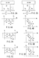
- FIGS. 1A and 1B are equivalent circuit diagrams, respectively, showing the memory cell structure of a ferroelectric non-volatile memory device;
- FIG. 2A is a circuit diagram showing a circuit arrangement of a memory operation analyzer using a MOSFET;
- FIG. 2B is a graph showing a change in drain current upon application of a read-out voltage;
- FIGS. 3A and 3B are equivalent circuit diagrams each showing the memory cell structure of the ferroelectric non-volatile memory device according to the embodiment of the present invention;
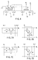
- FIGS. 4A and 4B are circuit diagrams each showing a state in which the memory cell of FIG. 3A or 3B is connected to a bit line BL, word line WL, and plate line PL;
- FIGS. 5A to 5D are circuit diagrams each showing a state in which a cell transistor is connected to lines in the cell structure of FIG. 4A or 4B;
- FIG. 6 is a sectional view showing an element structure for realizing the circuit arrangement shown in FIG. 5D;
- FIGS. 7A to 7D are circuit diagrams each showing a connection example when no common ground point exists;
- FIGS. 8A to 8D are plan views, respectively, showing cell arrangements for realizing the circuit arrangements of FIGS. 7A to 7D; and
- FIGS. 9A and 9B are a circuit diagram and a graph, respectively, for explaining the problem of a conventional ferroelectric non-volatile memory device.
-
- There will now be described a ferroelectric non-volatile memory device referring to FIGS. 1A and 1B.
- In an equivalent circuit representing the memory cell structure of a ferroelectric non-volatile memory device shown in FIGS. 1A and 1B, one terminal of each of two ferroelectric capacitors CA and CB having the same remanent polarization is connected to the gate of a cell transistor (MOSFET) Tr having a MOS structure. The other terminal of the capacitor CA is connected to a terminal A, whereas the other terminal of the capacitor CB is connected to a terminal B. The transistor Tr and the capacitors CA and CB constitute one memory cell. The ferroelectric films of the capacitors CA and CB are made of PZT, and have the same area and film thickness.
- The memory cell of this structure can also be used for an analog memory device. However, for descriptive convenience, the operation will be described by exemplifying a case in which the memory cell is used for a digital memory device. Although not shown, memory cells are arranged in a matrix to form a memory array.
- To write data "0" or "1" in the memory cell of this structure, the terminal B is grounded, and a positive or negative voltage is applied to the terminal A. When the influence of the potential on the semiconductor side cannot be ignored owing to a large gate capacitance of the transistor Tr, 1/2 the voltage applied to the terminal A is applied to set the potential of the semiconductor to a floating state or an intermediate potential between two series-connected ferroelectric capacitors.
- In this description, "1" is a state in which a positive voltage is applied to the terminal A to make the polarization direction of the ferroelectric capacitor CA downward and the polarization direction of the ferroelectric capacitor CB upward, as shown in FIG. 1A. "0" is a state in which a negative voltage is applied to the terminal A to make the polarization direction of the ferroelectric capacitor CA upward and the polarization direction of the ferroelectric capacitor CB downward, as shown in FIG. 1B.
- When the voltage of the terminal A is reset to 0 after "0" or "1" is written, no electric charges are induced to the gate electrode of the transistor Tr and the semiconductor surface of the channel region because the two ferroelectric capacitors CA and CB have the same remanent polarization. Accordingly, VG is kept to 0V from the relation of
- To read data written in the memory cell, the terminal A is opened, the semiconductor substrate is grounded, and a positive voltage is applied to the terminal B. In this case, when written data is "1", as shown in FIG. 1A, the polarization amount of the ferroelectric capacitor CB greatly changes, and the electric charges QG of the gate electrode change from 0. Letting P be the polarization amount of the ferroelectric thin film upon application of a positive voltage,
- When written data is "0", no polarization reversal of the ferroelectric thin film occurs. Even for a sufficiently large positive application voltage, only (PS - Pr)S electric charges QG are generated in the gate electrode. Since the difference between PS and Pr is generally small, almost no negative electric charges are induced to the semiconductor surface. In this case, the source-drain path of the transistor Tr does not flow any current.
- Thus, data can be read by applying a pulse voltage to the terminal B and measuring the drain current of the MOSFET at this time. In read, the voltage is applied through the gate insulator film of the MOSFET, and the read-out voltage may rise. However, this read-out voltage need not be applied until
- After read, both the terminals A and B are reset to 0V. For written data "0", QG = 0 holds, and the state returns to one before read. For written data "1", the polarization does not perfectly return to the original one when the read-out voltage is reset to 0. For this reason, data "1" is rewritten based on read-out data at a proper frequency.
- In this structure, the terminal B is grounded, a positive or negative voltage is applied to the terminal A, and the ferroelectric thin films of the ferroelectric capacitors CA and CB are polarized in opposite directions with respect to the gate electrode. Data can be stored in accordance with the polarization direction and remanent polarization of the ferroelectric thin film without inducing electric charges generated upon polarization of the ferroelectric thin film to the channel region. Since the internal electric fields of the two ferroelectric capacitors CA and CB are 0 regardless of whether data is held in a "0" or "1" state, the data retention time can be prolonged. Since the voltage is directly applied to the ferroelectric thin film, the data write-in voltage can be decreased.
- The results of analyzing the characteristics of a transistor with this structure using a circuit simulator SPICE will be described. FIG. 2A shows a circuit used for operation analysis, and FIG. 2B shows a change in drain current upon application of a read-out pulse.
- While switches SW0, SW1, and SW2 are OFF, ON, and OFF, respectively, a positive or negative voltage is applied to a terminal n2 to store data "0' or "1". The switches SW0, SW1, and SW2 are respectively turned off, on, and on, thereby holding the memory state. The switches SW0, SW1, and SW2 are respectively turned on, off, and off, and a voltage is applied to a terminal n0 to read out data. From FIGS. 2A and 2B, data "0" or "1" can be easily read out by measuring the drain current.
- An embodiment of the present invention will be described in detail with reference to the several views of the accompanying drawing.
- This embodiment adds, to the structure of FIGS. 1A and 1B, a selector transistor comprised of a MOSFET so as not to influence an unselected cell by the write-in voltage.
- The MOSFET serving as a switch for selective write operation is connected to the portion (FIG. 3A) of the terminal A (or terminal B) in FIGS. 1A and 1B, or at a portion (FIG. 3B) between the gate and one capacitor. In other words, in the structure shown in FIG. 3A, the gate of a cell transistor Q1 is connected to the node of the capacitors CA and CB connected in series to each other. A selector transistor Q2 is connected between a capacitor CB and a terminal b. The terminals a, b and c are connected a driver DR. In the structure shown in FIG. 3B, a selector transistor Q2 is between the gate of the cell transistor Q1 and the capacitor CB.
- Regardless of whether the selector transistor is connected to either of the two positions shown in FIGS. 3A and 3B, the same effects can be obtained as far as the selector transistor is kept off when the cell is not selected. In terms of the manufacture, the structure of FIG. 3A is superior because two capacitors can be directly formed on the floating gate electrode of the cell transistor. This embodiment will examine an arrangement in which the structure of FIG. 3A is processed as a unit cell.
- According to the structure shown in FIG. 3A, in write, a voltage applied to the terminal c turns on/off the selector transistor Q2 to control whether a voltage appearing between the terminals a and b is actually applied to the ferroelectric capacitors CA and CB. Accordingly, voltages at the terminals a, b, and c must be independently controlled from a peripheral circuit. Constituting this memory cell array requires at least three control lines a', b', and c'. If the lines b' and c' are parallel to each other, cells connected to them similarly operate, and do not play the role as a selector switch. Hence, the lines b' and c' must cross each other, and the three lines are arranged as shown in FIG. 4A or 4B. According to convention, the lines a', b', and c' will be referred to as a plate line (PL), bit line (BL), and word line (WL).
- In FIG. 4A, one terminal of the capacitor CA is connected to the gate electrode of the cell transistor Q1, and the other terminal is connected to the plate line PL. One terminal of the capacitor CB is connected to the gate electrode of the cell transistor Q1, and the other terminal is connected to the bit line BL via the selector transistor Q2. The gate electrode of the selector transistor Q2 is connected to the word line WL. In FIG. 4B, the connection is the same except that the plate line PL is parallel to the word line WL.
- Read operation will be explained. In read, the terminal of one capacitor is opened, the polarization of the other capacitor is reversed, and a current flowing through the d-e path at this time is detected. A new current detection line may be arranged, which is not preferable for a high cell arrangement density. Thus, the terminal d is connected to one of the word line WL, bit line BL, and plate line PL, and the terminal e is grounded. A case in which no common ground point exists, like an SOI (Si film on an insulator) substrate, will also be considered at last.
- When the polarization is reversed via the plate line PL without the mediacy of the selector transistor Q2 for cell selection, the line connected to the terminal d must cross the plate line PL. On the other hand, when the polarization is reversed via the bit line BL, the plate line PL must be open, and thus the terminal d cannot be connected to the plate line PL. Therefore, available connection methods are limited to four methods shown in FIGS. 5A to 5D.
- In FIG. 5A, in addition to the structure of FIG. 4A, the source of the cell transistor Q1 is grounded, and its drain is connected to the word line WL. In FIG. 5B, in addition to the structure of FIG. 4B, the source of the cell transistor Q1 is grounded, and its drain is connected to the bit line BL. In FIG. 5C, in addition to the structure of FIG. 4A, the source of the cell transistor Q1 is grounded, and its drain is connected to the bit line BL. In FIG. 5D, in addition to the structure of FIG. 4B, the source of the cell transistor Q1 is grounded, and its drain is connected to the word line WL.
- A structure in which the source of the cell transistor Q1 is grounded, and its drain is connected to the word line WL, like the connection of FIG. 5D, is shown in the sectional view of a device structure in FIG. 6. An n-channel MOS transistor (cell transistor) Q1 made up of n-
type diffusion regions 62 and agate electrode 63, and an n-channel MOS transistor (selector transistor) Q2 made up of n-type diffusion regions 64 and agate electrode 65 are formed on a p-type Si substrate 61 so as to be adjacent to each other.Capacitor electrodes gate electrode 63 of the cell transistor Q1 via aferroelectric film 66 and formed of ferroelectric thin films, thereby constituting the two ferroelectric capacitors CA and CB. - If no common ground point exists, like an SOI substrate, a line grounded in read can be used. Connection methods in this case are shown in FIGS. 7A to 7D. In FIGS. 7A to 7D, some of the methods use the line of an adjacent cell in consideration of an actual arrangement.
- In FIG. 7A, unlike FIG. 5A, the source of the cell transistor Q1 is not grounded but is connected to a bit line BL2 of an adjacent cell parallel to a bit line BL1 connected to the selector transistor Q2. In FIG. 7B, unlike FIG. 5B, the source of the cell transistor Q1 is not grounded but is connected to the word line WL. In FIG. 7C, unlike FIG. 5C, the source of the cell transistor Q1 is not grounded but is connected to the word line WL. In FIG. 7D, unlike FIG. 5D, the source of the cell transistor Q1 is not grounded but is connected to the bit line BL2 of an adjacent cell parallel to the bit line BL1 connected to the selector transistor Q2.
- Examples of the cell arrangement in this case are shown in FIGS. 8A to 8D. FIGS. 8A to 8D correspond to FIGS. 7A to 7D, respectively. As is apparent from FIGS. 8A to 8D, circuit arrangements as shown in FIGS. 7A to 7D can be laid out on the substrate without any change.
- According to this embodiment, in addition to the cell structure as shown in FIG. 1, the selector transistor Q2 is connected to the terminal of the ferroelectric capacitor CB opposite to the cell transistor, i.e., between the ferroelectric capacitor CB and the bit line BL. As a result, the data retention time can be prolonged, and the data write-in voltage can be decreased. Moreover, an unselected cell can be prevented from being influenced by the write-in voltage. As a result, the reliability of the memory cell can be improved.
- The present invention is not limited to the above-described embodiment. This embodiment uses PZT as the ferroelectric material of the ferroelectric capacitor, but the ferroelectric material is not limited to this. Any ferroelectric material can be used. Two ferroelectric capacitors connected to the gate electrode of a MOS transistor may have different ferroelectric film thicknesses, but their material and area must be the same.
- The field effect transistor is not limited to a MOS transistor, and can be a MIS transistor using a gate insulator film instead of a gate oxide film. Further, the Si stripe is not limited to an npn stripe, and may be a pnp stripe for formation of a p-channel transistor.
- As has been described above in detail, according to the present invention, a memory cell structure is formed by connecting two ferroelectric capacitors having almost the same remanent polarization to the gate electrode of a MOS or MIS field effect transistor. Data is stored by polarizing the ferroelectric thin films of the capacitors in opposite directions with respect to the gate electrode of the transistor. Since the voltage is directly applied to the ferroelectric thin film, the data write-in voltage can be decreased. At the same time, electric charges generated upon polarization of the ferroelectric thin film are not induced to the semiconductor surface of the channel region of the transistor. Since the internal electric fields of the two ferroelectric capacitors are 0 in a steady state after data is stored, the data retention time can be prolonged.
- In addition, since the selector transistor is connected to one ferroelectric capacitor opposite to the cell transistor, an unselected cell can be prevented from being influenced by the write-in voltage.
Claims (18)
- A ferroelectric non-volatile memory device characterized by comprising:a MOS or MIS cell transistor (Q1) having a gate electrode;two ferroelectric capacitors (CA, CB) which are connected to the gate electrode of said cell transistor and have substantially the same remanent polarization; anda selector transistor (Q2) connected to one of said capacitors,
wherein data is stored by polarizing ferroelectric thin films of said capacitors in opposite directions with respect to the gate electrode of said cell transistor. - The memory device according to claim 1, characterized in that one of said capacitors (CA, CB) has one terminal connected to the gate electrode of said cell transistor (Q1) and the other terminal connected to a bit line (BL) via said selector transistor (Q2), the other capacitor has one terminal connected to the gate electrode of said cell transistor and the other terminal connected to a plate line (PL), and the gate electrode of said selector transistor is connected to a word line (WL).
- A ferroelectric non-volatile memory device characterized by comprising:a cell transistor (Q1) constituted by a field effect transistor having a gate electrode;two ferroelectric capacitors (CA, CB) which are series-connected to each other, connected to the gate electrode of said cell transistor, and have substantially the same remanent polarization;a selector transistor (Q2) connected to one of said capacitors; anda driver (DR) for polarizing ferroelectric thin films of said capacitors in opposite directions with respect to the gate electrode of said cell transistor to store data.
- The memory device according to claim 3, characterized in that in data write, said driver (DR) applies a voltage to the gate electrode of said selector transistor (Q2) in order to turn on said selector transistor, and generates a voltage for causing polarization corresponding to the data in said capacitors (CA, CB) via said selector transistor.
- The memory device according to claim 4, characterized in that in data read, said driver (DR) applies a voltage pulse to one terminal of each capacitor via said selector transistor (Q2) in order to read out data corresponding to a polarization direction of said capacitor.
- The memory device according to claim 3, characterized in that said selector transistor (Q2) is connected between one terminal of one of said capacitors (CA, CB) and the gate electrode of said cell transistor (Q1).
- The memory device according to claim 3, characterized in that said selector transistor (Q2) is connected between one terminal of one of said capacitors (CA, CB) and a feeding terminal.
- The memory device according to claim 3, characterized in that said memory device further comprises a plate line (PL), a bit line (BL), and a word line (WL), said capacitors include first and second capacitors (CA, CB), said first capacitor (CA) has one terminal connected to the gate electrode of said cell transistor (Q1) and the other terminal connected to said plate line (PL), said second capacitor (CB) has one terminal connected to the gate electrode of said cell transistor and the other terminal connected to said bit line via said selector transistor, and the gate electrode of said selector transistor (Q2) is connected to said word line (WL).
- The memory device according to claim 8, characterized in that said bit line (BL) and said plate line (PL) are arranged to be parallel to each other, and cross said word line (WL).
- The memory device according to claim 8, characterized in that said word line (WL) and said plate line (PL) are arranged to be parallel to each other, and cross said bit line (BL).
- The memory device according to claim 9 or 10, characterized in that said cell transistor (Q1) has a grounded source and a drain connected to said word line (WL).
- The memory device according to claim 9 or 10, characterized in that said cell transistor (Q1) has a grounded source and a drain connected to said bit line (BL).
- The memory device according to claim 9 or 10, characterized in that said cell transistor (Q1) has a source connected to said word line (WL) and a drain connected to said bit line (BL).
- The memory device according to claim 9 or 10, characterized in that said cell transistor (Q1) has a source connected to another bit line (BL2) adjacent to said bit line (BL1), and a drain connected to said word line (WL).
- A ferroelectric non-volatile memory device characterized by comprising:a cell transistor (Q1) constituted by an n-channel MOS transistor having a p-type silicon substrate (61), a pair of first n-type diffusion regions (62) formed in the p-type silicon substrate, and a gate electrode (63) placed, with an insulating intermediate layer, over the p-type silicon substrate between the first n-type diffusion regions;a selector transistor (Q2) which is adjacent to said cell transistor (Q1), and is constituted by an n-channel MOS transistor having a pair of second n-type diffusion regions (64) formed in the p-type substrate, and a second gate electrode (65) placed, with an insulating intermediate layer, over the p-type silicon substrate between the second n-type diffusion regions; andtwo capacitors constituted by a ferroelectric film (66) formed on the gate electrode of said cell transistor, and two capacitor electrodes (67, 68) formed on said ferroelectric film,
wherein one of said capacitors is connected to one of the second n-type diffusion regions of said selector transistor. - The memory device according to claim 15, characterized in that said memory device further comprises a plate line (PL) connected to the capacitor electrode of the other capacitor, a word line (WL) connected to the second gate electrode of said selector transistor (Q2), and a bit line (BL) connected to the other of the second n-type diffusion regions (64) of said selector transistor, and the first n-type diffusion regions (62) of said cell transistor are respectively grounded and connected to said word line.
- The memory device according to claim 15, further comprising a driver for polarizing the ferroelectric thin films (67, 68) of said capacitors in opposite directions with respect to the gate electrode of said cell transistor to store data.
- The memory device according to claim 17, characterized in that said driver comprises a driver unit for, in data write, applying a voltage to the gate electrode (65) of said selector transistor (Q2) to cause polarization corresponding to the data in said capacitors via said selector transistor in order to turn on said selector transistor, and in data read, applying a voltage pulse to one terminal of each capacitor via said selector transistor in order to read out data corresponding to a polarization direction of said capacitor.
Priority Applications (1)
| Application Number | Priority Date | Filing Date | Title |
|---|---|---|---|
| EP04017770A EP1473736A3 (en) | 1999-05-19 | 2000-05-03 | Ferroelectric non-volatile memory device |
Applications Claiming Priority (2)
| Application Number | Priority Date | Filing Date | Title |
|---|---|---|---|
| JP13851599A JP3377762B2 (en) | 1999-05-19 | 1999-05-19 | Ferroelectric nonvolatile memory |
| JP13851599 | 1999-05-19 |
Related Child Applications (1)
| Application Number | Title | Priority Date | Filing Date |
|---|---|---|---|
| EP04017770A Division EP1473736A3 (en) | 1999-05-19 | 2000-05-03 | Ferroelectric non-volatile memory device |
Publications (3)
| Publication Number | Publication Date |
|---|---|
| EP1054406A2 true EP1054406A2 (en) | 2000-11-22 |
| EP1054406A3 EP1054406A3 (en) | 2001-01-17 |
| EP1054406B1 EP1054406B1 (en) | 2005-04-06 |
Family
ID=15223961
Family Applications (2)
| Application Number | Title | Priority Date | Filing Date |
|---|---|---|---|
| EP04017770A Withdrawn EP1473736A3 (en) | 1999-05-19 | 2000-05-03 | Ferroelectric non-volatile memory device |
| EP00109433A Expired - Lifetime EP1054406B1 (en) | 1999-05-19 | 2000-05-03 | Ferroelectric non-volatile memory device |
Family Applications Before (1)
| Application Number | Title | Priority Date | Filing Date |
|---|---|---|---|
| EP04017770A Withdrawn EP1473736A3 (en) | 1999-05-19 | 2000-05-03 | Ferroelectric non-volatile memory device |
Country Status (6)
| Country | Link |
|---|---|
| US (2) | US6327172B1 (en) |
| EP (2) | EP1473736A3 (en) |
| JP (1) | JP3377762B2 (en) |
| KR (1) | KR100355779B1 (en) |
| DE (1) | DE60019191T2 (en) |
| TW (1) | TW454338B (en) |
Families Citing this family (25)
| Publication number | Priority date | Publication date | Assignee | Title |
|---|---|---|---|---|
| DE10031947B4 (en) * | 2000-06-30 | 2006-06-14 | Infineon Technologies Ag | Circuit arrangement for balancing different voltages on cable runs in integrated semiconductor circuits |
| US6720596B2 (en) | 2000-10-17 | 2004-04-13 | Matsushita Electric Industrial Co., Ltd. | Semiconductor device and method for driving the same |
| JP2002203913A (en) * | 2000-12-28 | 2002-07-19 | Hitachi Ltd | Semiconductor storage device and method of manufacturing the same |
| JP3522248B2 (en) * | 2001-10-15 | 2004-04-26 | ローム株式会社 | Semiconductor integrated circuit device |
| JP3740577B2 (en) * | 2001-12-20 | 2006-02-01 | 松下電器産業株式会社 | Negative potential generating circuit, negative potential generating device, and semiconductor device using the same |
| JP2003209179A (en) * | 2002-01-15 | 2003-07-25 | Fujitsu Ltd | Capacitative element and method for manufacturing the same |
| JP2003263886A (en) * | 2002-03-08 | 2003-09-19 | Fujitsu Ltd | Ferroelectric memory in which bit line capacity can be optimized |
| DE102004011432A1 (en) * | 2004-03-09 | 2005-09-29 | Infineon Technologies Ag | Semiconductor memory cell e.g. for field effect transistors, has ferroelectric material zone designed with different remanent ferroelectric polarization states |
| KR100660901B1 (en) * | 2005-12-22 | 2006-12-26 | 삼성전자주식회사 | Eeprom device having single gate structure, operation method of the eeprom and fabrication method of the eeprom |
| FR2904464A1 (en) | 2006-07-27 | 2008-02-01 | St Microelectronics Sa | EEPROM LOAD RETENTION CIRCUIT FOR TIME MEASUREMENT |
| FR2904463A1 (en) * | 2006-07-27 | 2008-02-01 | St Microelectronics Sa | PROGRAMMING A LOAD RETENTION CIRCUIT FOR TIME MEASUREMENT |
| JP5371752B2 (en) | 2006-07-27 | 2013-12-18 | エス テ マイクロエレクトロニクス エス アー | Circuit to read charge holding elements for time measurement |
| WO2008012459A2 (en) * | 2006-07-27 | 2008-01-31 | Stmicroelectronics Sa | Charge retention circuit for time measurement |
| US7991041B2 (en) * | 2006-11-15 | 2011-08-02 | Qualcomm, Incorporated | Iterative detection and cancellation for wireless communication |
| US8781043B2 (en) * | 2006-11-15 | 2014-07-15 | Qualcomm Incorporated | Successive equalization and cancellation and successive mini multi-user detection for wireless communication |
| US7700985B2 (en) * | 2008-06-24 | 2010-04-20 | Seagate Technology Llc | Ferroelectric memory using multiferroics |
| WO2011063567A1 (en) | 2009-11-27 | 2011-06-03 | Qualcomm Incorporated | Interference cancellation for non-orthogonal channel sets |
| US8867256B2 (en) * | 2012-09-25 | 2014-10-21 | Palo Alto Research Center Incorporated | Systems and methods for writing and non-destructively reading ferroelectric memories |
| US20160005749A1 (en) * | 2014-07-01 | 2016-01-07 | Qualcomm Incorporated | Series ferroelectric negative capacitor for multiple time programmable (mtp) devices |
| US11088170B2 (en) | 2019-11-25 | 2021-08-10 | Sandisk Technologies Llc | Three-dimensional ferroelectric memory array including integrated gate selectors and methods of forming the same |
| US11335391B1 (en) | 2020-10-30 | 2022-05-17 | Ferroelectric Memory Gmbh | Memory cell arrangement and method thereof |
| US11527551B2 (en) * | 2020-10-30 | 2022-12-13 | Ferroelectric Memory Gmbh | Memory cell arrangements and methods thereof |
| US11380695B2 (en) | 2020-10-30 | 2022-07-05 | Ferroelectric Memory Gmbh | Memory cell arrangement and method thereof |
| WO2022094814A1 (en) * | 2020-11-04 | 2022-05-12 | 华为技术有限公司 | Ferroelectric memory and storage device |
| US20230326923A1 (en) * | 2021-11-01 | 2023-10-12 | KYOCERA AVX Components Corporation | Combined MOS/MIS Capacitor Assembly |
Citations (3)
| Publication number | Priority date | Publication date | Assignee | Title |
|---|---|---|---|---|
| US5523964A (en) * | 1994-04-07 | 1996-06-04 | Symetrix Corporation | Ferroelectric non-volatile memory unit |
| US5856688A (en) * | 1997-05-09 | 1999-01-05 | Samsung Electronics Co., Ltd. | Integrated circuit memory devices having nonvolatile single transistor unit cells therein |
| US6046929A (en) * | 1998-04-06 | 2000-04-04 | Fujitsu Limited | Memory device with two ferroelectric capacitors per one cell |
Family Cites Families (9)
| Publication number | Priority date | Publication date | Assignee | Title |
|---|---|---|---|---|
| JP2788265B2 (en) | 1988-07-08 | 1998-08-20 | オリンパス光学工業株式会社 | Ferroelectric memory, driving method and manufacturing method thereof |
| JP3021614B2 (en) | 1990-11-06 | 2000-03-15 | オリンパス光学工業株式会社 | Memory element |
| JPH07122661A (en) | 1993-10-27 | 1995-05-12 | Olympus Optical Co Ltd | Ferroelectric memory device |
| WO1995026570A1 (en) | 1994-03-29 | 1995-10-05 | Olympus Optical Co., Ltd. | Ferroelectric memory device |
| JPH08180673A (en) | 1994-12-27 | 1996-07-12 | Nec Corp | Ferroelectric memory cell and access device therefor |
| JPH1117123A (en) | 1997-06-23 | 1999-01-22 | Rohm Co Ltd | Non-volatile memory element |
| JPH1117112A (en) | 1997-06-24 | 1999-01-22 | Oki Electric Ind Co Ltd | Chip layout method for semiconductor integrated circuit |
| JP3495905B2 (en) * | 1998-02-19 | 2004-02-09 | シャープ株式会社 | Semiconductor storage device |
| US6198652B1 (en) * | 1998-04-13 | 2001-03-06 | Kabushiki Kaisha Toshiba | Non-volatile semiconductor integrated memory device |
-
1999
- 1999-05-19 JP JP13851599A patent/JP3377762B2/en not_active Expired - Fee Related
-
2000
- 2000-05-03 DE DE60019191T patent/DE60019191T2/en not_active Withdrawn - After Issue
- 2000-05-03 EP EP04017770A patent/EP1473736A3/en not_active Withdrawn
- 2000-05-03 EP EP00109433A patent/EP1054406B1/en not_active Expired - Lifetime
- 2000-05-05 TW TW089108596A patent/TW454338B/en not_active IP Right Cessation
- 2000-05-08 KR KR1020000024357A patent/KR100355779B1/en not_active IP Right Cessation
- 2000-05-09 US US09/567,865 patent/US6327172B1/en not_active Expired - Fee Related
-
2001
- 2001-10-04 US US09/971,988 patent/US6584008B2/en not_active Expired - Fee Related
Patent Citations (3)
| Publication number | Priority date | Publication date | Assignee | Title |
|---|---|---|---|---|
| US5523964A (en) * | 1994-04-07 | 1996-06-04 | Symetrix Corporation | Ferroelectric non-volatile memory unit |
| US5856688A (en) * | 1997-05-09 | 1999-01-05 | Samsung Electronics Co., Ltd. | Integrated circuit memory devices having nonvolatile single transistor unit cells therein |
| US6046929A (en) * | 1998-04-06 | 2000-04-04 | Fujitsu Limited | Memory device with two ferroelectric capacitors per one cell |
Also Published As
| Publication number | Publication date |
|---|---|
| EP1054406B1 (en) | 2005-04-06 |
| DE60019191D1 (en) | 2005-05-12 |
| DE60019191T2 (en) | 2006-03-09 |
| TW454338B (en) | 2001-09-11 |
| EP1054406A3 (en) | 2001-01-17 |
| EP1473736A2 (en) | 2004-11-03 |
| KR100355779B1 (en) | 2002-10-19 |
| KR20000077182A (en) | 2000-12-26 |
| US20020012264A1 (en) | 2002-01-31 |
| US6327172B1 (en) | 2001-12-04 |
| JP3377762B2 (en) | 2003-02-17 |
| US6584008B2 (en) | 2003-06-24 |
| EP1473736A3 (en) | 2006-10-04 |
| JP2000331484A (en) | 2000-11-30 |
Similar Documents
| Publication | Publication Date | Title |
|---|---|---|
| EP1054406B1 (en) | Ferroelectric non-volatile memory device | |
| US6188600B1 (en) | Memory structure in ferroelectric nonvolatile memory and readout method therefor | |
| US5523964A (en) | Ferroelectric non-volatile memory unit | |
| US6370056B1 (en) | Ferroelectric memory and method of operating same | |
| US6714435B1 (en) | Ferroelectric transistor for storing two data bits | |
| US7215567B2 (en) | Ferroelectric memory device | |
| US6898105B2 (en) | Ferroelectric non-volatile memory device having integral capacitor and gate electrode, and driving method of a ferroelectric non-volatile memory device | |
| US7123503B2 (en) | Writing to ferroelectric memory devices | |
| US6285577B1 (en) | Non-volatile memory using ferroelectric capacitor | |
| WO2010097862A1 (en) | Semiconductor memory cells and manufacturing method therefor as well as semiconductor memory devices | |
| US7167386B2 (en) | Ferroelectric memory and operating method therefor | |
| US6456520B1 (en) | Semiconductor memory and method for driving the same | |
| US6344991B1 (en) | Nonvolatile semiconductor memory device | |
| US6888736B2 (en) | Ferroelectric transistor for storing two data bits | |
| KR100478259B1 (en) | Nonvolatile memory and method of driving nonvolatile memory | |
| JP3131340B2 (en) | Ferroelectric memory element | |
| US6455883B2 (en) | Nonvolatile semiconductor memory | |
| Tsai et al. | Mechanism for slow switching effect in advanced low-voltage, high-speed Pb (Zr/sub 1-x/Ti/sub x/) O/sub 3/ferroelectric memory |
Legal Events
| Date | Code | Title | Description |
|---|---|---|---|
| PUAI | Public reference made under article 153(3) epc to a published international application that has entered the european phase |
Free format text: ORIGINAL CODE: 0009012 |
|
| 17P | Request for examination filed |
Effective date: 20000503 |
|
| AK | Designated contracting states |
Kind code of ref document: A2 Designated state(s): DE FR |
|
| AX | Request for extension of the european patent |
Free format text: AL;LT;LV;MK;RO;SI |
|
| PUAL | Search report despatched |
Free format text: ORIGINAL CODE: 0009013 |
|
| AK | Designated contracting states |
Kind code of ref document: A3 Designated state(s): AT BE CH CY DE DK ES FI FR GB GR IE IT LI LU MC NL PT SE |
|
| AX | Request for extension of the european patent |
Free format text: AL;LT;LV;MK;RO;SI |
|
| RIC1 | Information provided on ipc code assigned before grant |
Free format text: 7G 11C 11/22 A, 7G 11C 27/02 B |
|
| AKX | Designation fees paid |
Free format text: AT BE |
|
| RBV | Designated contracting states (corrected) |
Designated state(s): DE FR |
|
| REG | Reference to a national code |
Ref country code: DE Ref legal event code: 8566 |
|
| 17Q | First examination report despatched |
Effective date: 20040122 |
|
| GRAP | Despatch of communication of intention to grant a patent |
Free format text: ORIGINAL CODE: EPIDOSNIGR1 |
|
| GRAS | Grant fee paid |
Free format text: ORIGINAL CODE: EPIDOSNIGR3 |
|
| GRAA | (expected) grant |
Free format text: ORIGINAL CODE: 0009210 |
|
| AK | Designated contracting states |
Kind code of ref document: B1 Designated state(s): DE FR |
|
| REF | Corresponds to: |
Ref document number: 60019191 Country of ref document: DE Date of ref document: 20050512 Kind code of ref document: P |
|
| PLBE | No opposition filed within time limit |
Free format text: ORIGINAL CODE: 0009261 |
|
| STAA | Information on the status of an ep patent application or granted ep patent |
Free format text: STATUS: NO OPPOSITION FILED WITHIN TIME LIMIT |
|
| ET | Fr: translation filed | ||
| 26N | No opposition filed |
Effective date: 20060110 |
|
| PGFP | Annual fee paid to national office [announced via postgrant information from national office to epo] |
Ref country code: DE Payment date: 20070730 Year of fee payment: 8 |
|
| PG25 | Lapsed in a contracting state [announced via postgrant information from national office to epo] |
Ref country code: DE Free format text: LAPSE BECAUSE OF THE APPLICANT RENOUNCES Effective date: 20080103 |
|
| PGFP | Annual fee paid to national office [announced via postgrant information from national office to epo] |
Ref country code: FR Payment date: 20070426 Year of fee payment: 8 |
|
| REG | Reference to a national code |
Ref country code: FR Ref legal event code: ST Effective date: 20090119 |
|
| PG25 | Lapsed in a contracting state [announced via postgrant information from national office to epo] |
Ref country code: FR Free format text: LAPSE BECAUSE OF NON-PAYMENT OF DUE FEES Effective date: 20080602 |