EP1050816A2 - Microcomputer having built-in nonvolatile memory and check system thereof - Google Patents
Microcomputer having built-in nonvolatile memory and check system thereof Download PDFInfo
- Publication number
- EP1050816A2 EP1050816A2 EP00303065A EP00303065A EP1050816A2 EP 1050816 A2 EP1050816 A2 EP 1050816A2 EP 00303065 A EP00303065 A EP 00303065A EP 00303065 A EP00303065 A EP 00303065A EP 1050816 A2 EP1050816 A2 EP 1050816A2
- Authority
- EP
- European Patent Office
- Prior art keywords
- microcomputer
- nonvolatile memory
- test
- built
- test program
- Prior art date
- Legal status (The legal status is an assumption and is not a legal conclusion. Google has not performed a legal analysis and makes no representation as to the accuracy of the status listed.)
- Ceased
Links
Images



Classifications
-
- G—PHYSICS
- G06—COMPUTING OR CALCULATING; COUNTING
- G06F—ELECTRIC DIGITAL DATA PROCESSING
- G06F11/00—Error detection; Error correction; Monitoring
- G06F11/22—Detection or location of defective computer hardware by testing during standby operation or during idle time, e.g. start-up testing
- G06F11/26—Functional testing
-
- G—PHYSICS
- G06—COMPUTING OR CALCULATING; COUNTING
- G06F—ELECTRIC DIGITAL DATA PROCESSING
- G06F11/00—Error detection; Error correction; Monitoring
- G06F11/22—Detection or location of defective computer hardware by testing during standby operation or during idle time, e.g. start-up testing
- G06F11/26—Functional testing
- G06F11/263—Generation of test inputs, e.g. test vectors, patterns or sequences ; with adaptation of the tested hardware for testability with external testers
- G06F11/2635—Generation of test inputs, e.g. test vectors, patterns or sequences ; with adaptation of the tested hardware for testability with external testers using a storage for the test inputs, e.g. test ROM, script files
-
- G—PHYSICS
- G01—MEASURING; TESTING
- G01R—MEASURING ELECTRIC VARIABLES; MEASURING MAGNETIC VARIABLES
- G01R31/00—Arrangements for testing electric properties; Arrangements for locating electric faults; Arrangements for electrical testing characterised by what is being tested not provided for elsewhere
- G01R31/28—Testing of electronic circuits, e.g. by signal tracer
- G01R31/317—Testing of digital circuits
- G01R31/3181—Functional testing
- G01R31/319—Tester hardware, i.e. output processing circuits
- G01R31/31917—Stimuli generation or application of test patterns to the device under test [DUT]
- G01R31/31926—Routing signals to or from the device under test [DUT], e.g. switch matrix, pin multiplexing
-
- G—PHYSICS
- G06—COMPUTING OR CALCULATING; COUNTING
- G06K—GRAPHICAL DATA READING; PRESENTATION OF DATA; RECORD CARRIERS; HANDLING RECORD CARRIERS
- G06K19/00—Record carriers for use with machines and with at least a part designed to carry digital markings
- G06K19/06—Record carriers for use with machines and with at least a part designed to carry digital markings characterised by the kind of the digital marking, e.g. shape, nature, code
- G06K19/067—Record carriers with conductive marks, printed circuits or semiconductor circuit elements, e.g. credit or identity cards also with resonating or responding marks without active components
- G06K19/07—Record carriers with conductive marks, printed circuits or semiconductor circuit elements, e.g. credit or identity cards also with resonating or responding marks without active components with integrated circuit chips
-
- G—PHYSICS
- G06—COMPUTING OR CALCULATING; COUNTING
- G06K—GRAPHICAL DATA READING; PRESENTATION OF DATA; RECORD CARRIERS; HANDLING RECORD CARRIERS
- G06K19/00—Record carriers for use with machines and with at least a part designed to carry digital markings
- G06K19/06—Record carriers for use with machines and with at least a part designed to carry digital markings characterised by the kind of the digital marking, e.g. shape, nature, code
- G06K19/067—Record carriers with conductive marks, printed circuits or semiconductor circuit elements, e.g. credit or identity cards also with resonating or responding marks without active components
- G06K19/07—Record carriers with conductive marks, printed circuits or semiconductor circuit elements, e.g. credit or identity cards also with resonating or responding marks without active components with integrated circuit chips
- G06K19/073—Special arrangements for circuits, e.g. for protecting identification code in memory
-
- G—PHYSICS
- G06—COMPUTING OR CALCULATING; COUNTING
- G06K—GRAPHICAL DATA READING; PRESENTATION OF DATA; RECORD CARRIERS; HANDLING RECORD CARRIERS
- G06K7/00—Methods or arrangements for sensing record carriers, e.g. for reading patterns
- G06K7/0095—Testing the sensing arrangement, e.g. testing if a magnetic card reader, bar code reader, RFID interrogator or smart card reader functions properly
-
- G—PHYSICS
- G11—INFORMATION STORAGE
- G11C—STATIC STORES
- G11C29/00—Checking stores for correct operation ; Subsequent repair; Testing stores during standby or offline operation
- G11C29/52—Protection of memory contents; Detection of errors in memory contents
Definitions
- the present invention relates to a microcomputer having a built-in nonvolatile memory, an IC card packing the same, and a check system thereof.
- microcomputers having built-in nonvolatile memories are used extensively in electric appliances and OA (Office Automation) systems as data memories or program memories.
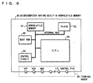
- a conventional typical microcomputer 80 comprises a nonvolatile memory 81, a RAM 82, a CPU 83, a control circuit 84, and a boot ROM 85, which are interconnected to each other via an internal bus.
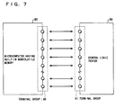
- a general logic tester or the like is used to test the above-arranged microcomputer 80. More specifically, as shown in Figure 7, a plurality of test terminals (terminal group 91) of a general logic tester 90 (hereinafter, referred to simply as tester 90) are connected to a plurality of test terminals (terminal group 86) of the microcomputer 80 in a one-to-one correspondence. Then, the microcomputer 80 is switched to the test mode by a signal from the tester 90, and a test is conducted on the internal circuits.
- test program is stored in the tester 90, and for this reason, in order to enable the tester 90 to give a data signal, an address signal, a clock signal, a control signal, etc. to the microcomputer 80, connecting means composed of at least tens of pins is necessary ( Figure 7).
- this test method using the tester 90 can not be applied when conducting a final test on the memory section of the completed product prior to shipment.
- a final check can be conducted only by a so-called actual test, by which the completed product is actually operated for a check-up.
- the check-up items available by the above test method are limited to writing, reading, and erasing with respect to the nonvolatile memory 81, and there is a problem that detailed check-up items, such as a shift quantity of a Vth voltage in each memory cell, can not be tested.
- the microcomputer 80 packed in the product could be connected to the tester 90 through connecting means composed of tens of pins, there arises another problem that the general tester can test only one chip at a time.
- the most advanced general logic tester can test more than one chip, but the number of chips is limited to a few at most.
- the nonvolatile memory 81 is to be tested in detail with high accuracy, the time required for the test and the number of check-up items are increased markedly compared with the conventional test method. Thus, it is essential to test a greater number of chips simultaneously to save the cost of the test.
- the IC card is defined as a card including a information data recording memory represented by a nonvolatile memory, and a microcomputer which controls the memory, wherein data and programs are stored in the memory while data is read out or written into the memory when necessary.
- EEPROMs Electrically Erasable and Programmable Read Only Memories
- Typical EEPROMs have a memory capacity of 8-16 Kbytes and data can be overwritten up to 10,000 times.
- the IC cards are used in diversified fields including electronic settlements of accounts, public transportation, medical, distributions, etc. For this reason, not only higher reliability, but also higher security against forgery are required for the IC cards.
- test is generally conducted on the chip per se, and another test is conducted further on the memory packed in the card.
- a generally adopted test method for the memory is as follows. That is, a test program is stored in the built-in ROM or test ROM during the manufacturing process, so that when a test command is entered from an external check device, the CPU starts to run the test program on the test ROM, whereby the test is conducted on the memory.
- Japanese Laid-open Patent Application No. 3082/1985 Japanese Laid-open Patent Application No. 3082/1985 (Japanese Official Gazette, Tokukaisho No . 60-3082 , publishing date: January 9, 1985) discloses a technique which realizes the test on the memory packed in the IC card. More specifically, an IC card is set in a certain check device and a test command signal is sent to the IC card from the check device, whereupon the CPU starts to run the test program prestored in the built-in ROM, thereby making it possible to conduct a test on the memory packed in the IC card.
- Japanese Laid-open Patent Application No. 193056/1985 Japanese Laid-open Patent Application No. 193056/1985 (Japanese Official Gazette, Tokukaisho No . 60-193056 , publishing date: October 1, 1985) discloses a similar technique.
- the above conventional technique essentially uses the test program written into the ROM, and therefore, the IC card has to additionally include the test ROM or secure a program area for the test program in the built-in ROM.
- the capacity secured for the test program is limited, there is a problem that a test can not be conducted in a satisfactory manner to ensure the reliability of the memory.
- the number of the tests conducted on the nonvolatile memory should be increased with the increasing reliability.
- a test should be conducted on the writing/reading/erasing margins by checking the Vth voltage in each memory cell.
- test program written into the ROM can not be overwritten.
- a capacity of the ROM has to be increased markedly.
- the check device and chip communicate in a one-to-one correspondence in the final stage.
- a large number of chips can not be tested at a time.
- a microcomputer having a built-in nonvolatile memory of the present invention is characterized by being furnished with:
- the test program for the nonvolatile memory is sent from the external check system through the communication circuit.
- the test program is run on the RAM, and the nonvolatile memory is tested in accordance with the test program.
- the test program for the nonvolatile memory is conventionally stored in the built-in ROM or test ROM during the manufacturing process so as to cut the check time shorter and make the check system simpler.
- the above conventional arrangement has a following problem. That is, the program written into the ROM can not be overwritten whereas a number of test programs should be written into the ROM but the ROM has a limited capacity. Hence, a sufficient number of programs can not be written into the ROM, thereby making it impossible to conduct a test in a satisfactory manner to prove high reliability of the nonvolatile memory.
- the program data is created and written into the ROM during the manufacturing process, the data can be readily analyzed.
- the conventional method that is, storing the test program in the ROM, is virtually exposing the security of the IC card to danger.
- the test program for the nonvolatile memory is sent from the external check system and run on the RAM.
- a number of test programs can be transferred temporarily to the RAM and run thereon without using a ROM in which the test programs has been written in advance. Consequently, a highly reliable test having a sufficient number of check-up items can be conducted without any restriction from a limited capacity of the ROM.
- test program transferred onto the RAM is erased as soon as the test is completed and the supply of the power source voltage is stopped.
- the test program is not left in the completed product, unauthorized analysis of the test program can be prevented.
- the foregoing is particularly effective for a product that requires high reliability and security, such as the IC card packing the microcomputer having a nonvolatile memory.
- a check system of the present invention of the microcomputer having a built-in nonvolatile memory is characterized by being furnished with:
- the external communication device and the microcomputer having a built-in nonvolatile memory are connected to each other in such a manner so as to allow a communication in a one-to-one correspondence.
- the external communication device stores the test program for the built-in nonvolatile memory in the microcomputer, and sends the same to the microcomputer having a built-in nonvolatile memory.
- test program it is not necessary to write the test program in the built-in ROM or test ROM in the microcomputer having a built-in nonvolatile memory in advance, because the test program can be sent from the external communication device. Consequently, a highly reliable test having a sufficient number of check-up items can be conducted without any restriction from a limited capacity of the ROM.
- a check system of a microcomputer 10 having a built-in nonvolatile memory of the present embodiment (hereinafter, referred to simply as microcomputer 10) comprises an external communication device 20 and a control computer 30.
- a check-up of a built-in nonvolatile memory 11 in the microcomputer 10 is conducted by connecting the external communication device 20 to both the microcomputer 10 and control computer 30 so as to allow mutual communications.
- the microcomputer 10 comprises the nonvolatile memory 11, a RAM (Random Access Memory) 12, a CPU (Central Processing Unit) 13, a communication circuit 14, a control circuit 15, and a boot ROM (Read Only Memory) 16, which are interconnected to each other via an internal bus.
- the microcomputer 10 further comprises a terminal group 17 including a VPP terminal 17a, a VCC terminal 17b, a GND terminal 17c, a RST terminal 17d, a CLK terminal 17e, and an I/O (Input/Output) terminal 17f.
- the CPU 13 runs a program stored in the boot ROM 16 and RAM 12.
- the communication circuit 14 and control circuit 15 mainly control communications with the external communication device 20 as to a flowing rate, protocols, etc.
- the boot ROM 16 positions (stores) only a program to operate the communication circuit 14 in such a manner so as to be run by the CPU 13. More specifically, the boot ROM 16 stores a program for the following jobs of:
- the test program for the nonvolatile memory 11 is transferred to the RAM 12 from the external communication device 20, stored in the RAM 12 and run by the CPU 13 in order to conduct a check-up of the nonvolatile memory 11.
- the external communication device 20 comprises a communication microcomputer 21, a communication control circuit 22, a power source circuit 23, and a storage device 25, which are interconnected to each other via an internal bus.
- the external communication device 20 further comprises a terminal group 24 including a VPP terminal 24a, a VCC terminal 24b, a GND terminal 24c, a RST terminal 24d, a CLK terminal 24e, and an I/O terminal 24f.
- the external communication device 20 and microcomputer 10 are connected to each other through the terminal group 17 and terminal group 24 in such a manner that the terminals in each group are connected to each other in a one-to-one correspondence.
- Power is supplied respectively from the VPP terminal 24a to the VPP terminal 17a and from the VCC terminal 24b to the VCC terminal 17b, and a clock is supplied from the CLK terminal 24e to the CLK terminal 17e.
- data communication is allowed between the I/O terminals 17f and 24f when necessary.
- the communication microcomputer 21 and communication control circuit 22 mainly control communications with the microcomputer 10 and control computer 30 as to a communication rate, protocols, etc.
- the power source circuit 23 is a power source which supplies a driving power to the external communication device 20 and the microcomputer 10 connected thereto through the VPP terminals 24a and 17a and VCC terminals 24b and 17b.
- the power necessary for the microcomputer 10 during the check-up of the nonvolatile memory 11 is supplied from the power source circuit 23 in the external communication device 20.
- a power source voltage currently supplied from the power source circuit 23 in the external communication device 20 is stopped, whereupon the test program stored in the RAM 12 is erased automatically.
- the storage device 25 is a memory which stores the test program for the built-in nonvolatile memory 11 in the microcomputer 10. In order to conduct the check-up of the nonvolatile memory 11, the test program is read out from the storage device 25 and sent to the microcomputer 10. The test program may be sent to the external communication device 20 from the control computer 30 and stored temporarily in the storage device 25 each time a check-up of the nonvolatile memory 11 is conducted.
- the external communication device 20 is controlled by an external device, namely, the control computer 30.
- the external communication device 20 may be controlled directly by the communication microcomputer 21.
- a plurality of external communication devices 20 may be connected to one control computer 30, so that a plurality of microcomputers 10 can be tested simultaneously.
- the IC card 1 is furnished with, on its surface, a terminal group 17' connected to the terminal group 17 in the microcomputer 10 in such a manner that the terminals in each group are connected to each other in a one-to-one correspondence.
- the external communication device 20 is connected to the terminal group 17 through connection between the terminals in the terminal group 24 and terminal group 17' in a one-to-one correspondence, whereby a communication with the microcomputer 10 is allowed.
- a plurality of the external communication devices 20 may be connected to one control computer 30, so that a plurality of IC cards 1 can be tested simultaneously.
- the microcomputer 10 is electrically connected to the external communication device 20 through the terminal groups 17 and 24 (terminal groups 17' and 24).
- the electrical connection may be established by means of direct physical contact or electric waves, such as electromagnetic waves, as long as communications are allowed.
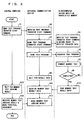
- control microcomputer 30 sends a command to the external communication device 20 to start the transfer of the test program for the nonvolatile memory 11 to the microcomputer 10 (S1 and S2).
- the external communication device 20 sends a signal (command) to the I/O terminal 17f of the microcomputer 10 to start the transfer of the test program (S3).
- the microcomputer 10 Upon receipt of the signal (test program transfer start command) (S4), the microcomputer 10 sets the conditions necessary for the transfer, such as area allocation in the RAM 12 for the transferred test program, whereby the microcomputer 10 becomes ready to receive data (test program).
- the test program is sent to the microcomputer 10 from the external communication device 20 through the I/O terminals 24f and 17f, and the microcomputer 10 stores the received test program in the RAM 12 (S5 and S6).
- the series of operations thus far are carried out by the CPU 13 as it runs the prestored program in the boot ROM 16 in the microcomputer 10.
- the CPU 13 confirms the completion of the transfer of the test program and switches the control onto a specific address in the RAM area, and starts to run the test program on the RAM 12 (S7). More specifically, the CPU 13 sets the nonvolatile memory 11 to the test mode, completes the check-up items one by one, and creates test result data including the test result, a fail log, etc.
- the CPU 13 Upon conformation of the completion of the memory test (S8), the CPU 13 sends the result data of the memory test to the external communication device 20 which has been waiting for the same (S9, S10, S11).
- the external communication device 20 makes the pass/fail judgment of the nonvolatile memory 11 based on the result data of the memory test sent from the microcomputer 10, and sends the judging result of the memory test to the control computer 30 which has been waiting for the same (S12, S13, S14).
- the test on the nonvolatile memory 11 is completed when the control microcomputer 30 receives the pass/fail judgement from the microcomputer 10 (S14).
- microcomputer 10 makes the pass/fail judgment by the self based on the test result data which had been created by the self or the control computer 30 does so based on the received test result data.
- the microcomputer having a built-in nonvolatile memory of the present embodiment comprises:
- the nonvolatile memory is switched to the test mode on the RAM, and consequently, highly reliable and secure test can be conducted on the built-in nonvolatile memory in the microcomputer.
- a plurality kinds of tests can be conducted by temporarily transferring the same on the RAM without using a conventionally essential exclusive-use ROM having stored the test program. Consequently, a highly reliable test, such as a margin test for the memory cell, can be conducted on the nonvolatile memory.
- test program transferred onto the RAM is erased as soon as the test is completed and the supply of the power source voltage is stopped.
- the test program is not left in the completed product, unauthorized analysis of the test program can be prevented. This is particularly effective for a product that requires high reliability and security, such as the IC card packing the foregoing microcomputer having a nonvolatile memory.
- a check system of a microcomputer 40 having a built-in nonvolatile memory (hereinafter, referred to simply as DUT (Device Under Test) 40) comprises a communication control microcomputer 50 (hereinafter referred to simply as microcomputer 50) and a control computer 30.
- DUT Device Under Test
- microcomputer 50 a communication control microcomputer 50
- a check-up of the built-in nonvolatile memory 11 in the DUT 40 is conducted when pairs of the DUTs 40 and microcomputers 50 are provided on a test board 60 in such a manner that (1) the DUT 40 and microcomputer 50 in each pair are connected to each other so as to allow mutual communications, and (2) all the DUTs 40 are connected to one control computer 30 so as to allow mutual communications.
- the DUT 40 and microcomputer 50 of the present embodiment are of the same structures as those of the microcomputer 10 and external communication device 20 of Embodiment 1, respectively.
- a plurality of microcomputers 50 and DUTs 40 are connected in such a manner so as to allow mutual communications in a one-to-one correspondence in each pair, and aligned in parallel on the test board 60.
- Each microcomputer 50 is connected to the computer 30 in such a manner so as to allow mutual communications individually.
- the check system is arranged in such a manner that it can additionally conduct a burn-in test by providing the DUTs 40 in a heater block 61. It does not cause any problem if the heat block 61 is realized by connecting the DUTs 40 and microcomputers 50 to each other through cables and placing the DUTs 40 in a hot temperature bath.
- FIG 5 is a view explaining the check system which checks IC card modules 41 instead of the DUTs 40 of Figure 4.
- Each IC card module 41 is of the same structure as that of the IC card 1 of Embodiment 1.
- the check system is arranged in such a manner that it can additionally conduct a burn-in test by providing the IC card modules 41 in the heater block 61. It does not cause any problem if the heat block 61 is realized by connecting the IC card modules 41 and microcomputers 50 to each other through cables and placing the IC card modules 41 in a hot temperature bath.
- the control computer 30 sends a test command to all the microcomputers 50 connected thereto simultaneously to start the transfer of the test program for the nonvolatile memory 11 to the DUTs 40 (S1).
- each microcomputer 50 Upon receipt of the test command, each microcomputer 50 processes the command, and confirms that the received command is the test command (S2).
- each microcomputer 50 Upon conformation of the test command, each microcomputer 50 sends a signal (command) to the corresponding DUT 40 to start the transfer of the necessary test program (S3).
- the DUT 40 Upon receipt of the signal (test program transfer start command) (S4), the DUT 40 sets the necessary conditions, such as area allocation for the transferred test program on the RAM 12, whereby it becomes ready to receive data (test program).
- each microcomputer 50 starts to send the test program, and the DUT 40 stores the received test program in the RAM 12 (S5, S6). It does not make any difference whether the test program is sent from the control computer 30 or the memory (equivalent to the storage device 25) in each microcomputer 50.
- the series of operations thus far are carried out by the CPU 13 as it runs the program prestored in the boot ROM 16 in the DUT 40.
- the CPU 13 in each DUT 40 confirms the completion of the transfer of the test program, and switches the control to a specific address in the RAM area, whereupon the CPU 13 starts to run the test program on the RAM 12 (S7). More specifically, the CPU 13 sets the nonvolatile memory to the test mode, carries out the check-up items one by one, and creates the test result data including the test result, a fail log, etc.
- the CPU 13 Upon confirming the completion of the memory test (S8), the CPU 13 sends the result data of the memory test to the microcomputer 50 which has been waiting for the same (S9, S10, S11).
- Each microcomputer 50 makes the pass/fail judgment of the nonvolatile memory 11 based on the result data of the memory test received from the corresponding DUT 40, and sends the judging result of the memory test to the control computer 30 which has been waiting for the same (S12, S13, S14).
- the control computer 30 completes the test on the nonvolatile memory 11 (S14).
- a plurality of the microcomputers equivalent to the external communication device of Embodiment 1 are aligned in parallel on the same test board, and all the microcomputers are connected to one system control computer.
- the check system of the IC card packing the microcomputer having a built-in nonvolatile memory a microcomputer different from the external communication device in the check system of Embodiment 1 is used as the external communication device, a plurality of external communication devices are aligned on the same board, and all the external communication devices are controlled intensively by connecting the same to another communication device (control computer). Consequently, the check system is arranged in such a manner that a plurality of microcomputers each having a built-in nonvolatile memory and a plurality of IC cards packing the same are tested simultaneously.
- the DUTs and microcomputers aligned on the same test board are controlled intensively, thereby making it possible to test a plurality of chips simultaneously. Consequently, the cost of the test can be saved markedly.
- the microcomputer having a built-in nonvolatile memory in each of Embodiments 1 and 2 is a microcomputer having an at least partially erasable built-in nonvolatile memory, which may be arranged in such a manner that, when a nonvolatile memory section is tested:
- the check system of the microcomputer having a nonvolatile memory in each of Embodiments 1 and 2 may be arranged in such a manner that, when a nonvolatile memory section of the above-arranged microcomputer having a nonvolatile memory is tested:
- a check system of the microcomputer having a nonvolatile memory in each of Embodiments 1 and 2 may be arranged in such a manner that, when a nonvolatile memory section of the above-arranged microcomputer having a nonvolatile memory is tested:
- a plurality of microcomputers each having a built-in nonvolatile memory can be tested simultaneously.
- the microcomputer having a built-in nonvolatile memory in each of Embodiments 1 and 2 may be packed in an IC card.
- a check system of the microcomputer having a nonvolatile memory in each of Embodiments 1 and 2 may be arranged in such a manner that, when a nonvolatile memory section in the above-arranged IC card is tested:
- a check system of the microcomputer having a nonvolatile memory in each of Embodiments 1 and 2 may be arranged in such a manner that, when a nonvolatile memory section of the microcomputer having a nonvolatile memory packed in the above-arranged IC card is tested:
- a plurality of the IC cards each packing the microcomputer having a built-in nonvolatile memory can be tested simultaneously.
- a microcomputer having a built-in nonvolatile memory of the present invention may comprise:
- a check system of the present invention of a microcomputer having a built-in nonvolatile memory may include an external communication device including:
- the microcomputer having a built-in nonvolatile memory receives the test program for the nonvolatile memory from the check system and stores the same in the RAM in accordance with the control program prestored in the boot ROM at a test command issued from the check system, and runs the test program, after which the microcomputer having a built-in nonvolatile memory sends the test result to the check system.
- the check system sends the test command from the external communication device to the microcomputer having a nonvolatile memory together with the test program stored in the storage device.
- the test program is run after the nonvolatile memory is switched to the test mode by the test program on the RAM, whereby a highly reliable and secure test can be conducted.
- a highly reliable test such as a margin test for the memory cell, can be conducted on the nonvolatile memory.
- test program transferred to the RAM is erased as soon as the test is completed and the supply of the power source voltage is stopped.
- the test program is not left in the completed product, unauthorized analysis of the test program can be prevented. This is particularly effective for a product that requires high reliability and security, such as the IC card packing the microcomputer having a nonvolatile memory.
- the microcomputer having a built-in nonvolatile memory and the check system thereof can conduct a highly reliable and secure test at a low cost without using the general tester and leaving the test program on the chip.
- the check system is arranged in such a manner that a plurality of external communication devices are controlled intensively by the control computer.
- the cost of the test can be saved significantly as an effect.
- the check system of the present invention of the microcomputer having a built-in nonvolatile memory may comprise:
- the built-in nonvolatile memories in a plurality of microcomputers are controlled intensively by the control computer, thereby making it possible to check a plurality of chips simultaneously.
- the costs of the check-up of the nonvolatile memory can be saved significantly.
- the foregoing effects are especially important for the IC cards each packing the microcomputer having a built-in nonvolatile memory of a large capacity for storing various kinds of information.
- An IC card of the present invention may be arranged to pack the above microcomputer having a built-in nonvolatile memory.
- a check system of the IC card packing the microcomputer having a built-in nonvolatile memory may comprise an external communication device including:
- the microcomputer having a built-in nonvolatile memory packed in the IC card receives the test program for the nonvolatile memory from the check system and stores the same in the RAM at a test command issued from the check system in accordance with the control program prestored in the boot ROM, and runs the test program, after which the microcomputer having a built-in nonvolatile memory sends the test result to the check system.
- the check system sends the test command to the microcomputer having a built-in nonvolatile memory packed in the IC card from the external communication device together with the test program stored in the storage device.
- a highly reliable and secure test can be conducted by switching the nonvolatile memory to the test mode by the test program on the RAM.
- a plurality kinds of tests can be conducted by temporarily transferring the same on the RAM without using a conventionally essential exclusive-use ROM having stored the test program. Consequently, a highly reliable test, such as a margin test for the memory cell, can be conducted on the nonvolatile memory.
- test program transferred to the RAM is erased as soon as the test is completed and the supply of the power source voltage is stopped.
- the test program is not left in the completed product, unauthorized analysis of the test program can be prevented. This is particularly effective for a product that requires high reliability and security, such as the IC card packing the microcomputer having a nonvolatile memory.
- the IC card packing the microcomputer having a nonvolatile memory and the check system thereof can conduct a highly reliable and secure test at a low cost without using the general tester and leaving the test program on the chip.
- the check system of the present invention of the IC card packing a microcomputer having a built-in nonvolatile memory may be arranged in such a manner so as to include a control computer, connected to a plurality of external communication devices, for intensively controlling a check-up of the IC cards connected to the plurality of the external communication devices, respectively.
- the built-in nonvolatile memories in a plurality of microcomputers packed in the IC cards are controlled intensively by using the control computer, thereby making it possible to check a plurality of the IC cards simultaneously.
- the cost of the check-up of the nonvolatile memory packed in the IC card can be saved significantly.
Landscapes
- Engineering & Computer Science (AREA)
- Theoretical Computer Science (AREA)
- Physics & Mathematics (AREA)
- General Physics & Mathematics (AREA)
- General Engineering & Computer Science (AREA)
- Computer Hardware Design (AREA)
- Microelectronics & Electronic Packaging (AREA)
- Quality & Reliability (AREA)
- Computer Security & Cryptography (AREA)
- Computer Networks & Wireless Communication (AREA)
- Artificial Intelligence (AREA)
- Computer Vision & Pattern Recognition (AREA)
- Test And Diagnosis Of Digital Computers (AREA)
- Credit Cards Or The Like (AREA)
- Microcomputers (AREA)
- Techniques For Improving Reliability Of Storages (AREA)
- For Increasing The Reliability Of Semiconductor Memories (AREA)
Abstract
Description
wherein the boot ROM has stored a control program for following jobs of:
Claims (15)
- A microcomputer having a built-in nonvolatile memory including:a communication circuit (14) for receiving a test program for a nonvolatile memory (11) from an external check system; anda RAM (12) on which said test program is run.
- The microcomputer having a built-in nonvolatile memory of Claim 1, further including a boot ROM (16) in which a control program for enabling receiving of said test program through said communication circuit (14) and running of said test program on said RAM (12).
- A microcomputer having a built-in nonvolatile memory including:a nonvolatile memory (11);a boot ROM (16);a RAM (12):a CPU (13) for running a program stored in said boot ROM (16) and RAM (12); anda communication circuit (14) for controlling a communication with a check system,said boot ROM (16) storing a control program for jobs of:receiving a test program for said nonvolatile memory (11) from said check system to be stored in said RAM (12) at a test command issued from said check system;running said test program; andsending a test result to said check system.
- A check system of a microcomputer having a built-in nonvolatile memory furnished with:at least one external communication device (20, 50) connected to said microcomputer (10, 40) in such a manner so as to allow a communication in a one-to-one correspondence,each external communication device (20, 50) including,a storage device (25) having stored a test program for a built-in nonvolatile memory (11) in said microcomputer (10, 40), anda communication microcomputer (21) for sending said test program to said microcomputer (10, 40).
- The check system of Claim 4, further furnished with a control computer (30), connected to a plurality of external communication devices (20, 50), for intensively controlling a check-up of a plurality of microcomputers (10, 40) each having a built-in nonvolatile memory and connected to said plurality of external communication devices (20, 50), respectively.
- A check system of a microcomputer having a built-in nonvolatile memory furnished with an external communication device (20, 50) including:a storage device (25) having stored a test program for said microcomputer (10, 40) having a built-in nonvolatile memory (11);a communication control circuit (22) for controlling a communication with said microcomputer (10, 40); anda communication microcomputer (21) for sending said test program to said microcomputer (10, 40) when checking the built-in nonvolatile memory (11) therein.
- The check system of Claim 6, further furnished with a control computer (30), connected to a plurality of external communication devices (20, 50), for intensively controlling a check-up of a plurality of microcomputers (10, 40) each having a built-in nonvolatile memory and connected to said plurality of external communication devices (20, 50), respectively.
- An IC card packing a microcomputer having a built-in nonvolatile memory including:a communication circuit (14) for receiving a test program for a nonvolatile memory (11) from an external check system; anda RAM (12) on which said test program is run.
- The IC card of Claim 8, further including a boot ROM (16) in which a control program for enabling receiving of said test program through said communication circuit (14) and running of said test program on said RAM (12).
- An IC card packing a microcomputer having a built-in nonvolatile memory including:a nonvolatile memory (11);a boot ROM (16);a RAM (12);a CPU (13) for running a program stored in said boot ROM (16) and RAM (12); anda communication circuit (14) for controlling a communication with a check system,said boot ROM (16) storing a control program for jobs of:receiving a test program for said nonvolatile memory (11) from said check system to be stored in said RAM (12) at a test command issued from said check system;running said test program; andsending a test result to said check system.
- A check system of an IC card packing a microcomputer having a built-in nonvolatile memory furnished with:at least one external communication device (20, 50) connected to said microcomputer (10, 40) packed in said IC card (1, 41) in such a manner so as to allow a communication in a one-to-one correspondence,each external communication device (20, 50) including,a storage device (25) having stored a test program for a built-in nonvolatile memory (11) in said microcomputer (10, 40), anda communication microcomputer (21) for sending said test program to said IC card (1, 41).
- The check system of Claim 11, further furnished with a control computer (30), connected to a plurality of external communication devices (20, 50), for intensively controlling a check-up of a plurality of IC cards (1, 41) connected to said plurality of external communication devices (20, 50), respectively.
- A check system of an IC card packing a microcomputer having a built-in nonvolatile memory furnished with an external communication device (20, 50) including:a storage device (25) having stored a test program for a built-in nonvolatile memory (11) in said microcomputer (10, 40) packed in said IC card (1, 41);a communication control circuit (22) for controlling a communication with said IC card (1, 41); anda communication microcomputer (21) for sending said test program to said IC card (1, 41) when checking said built-in nonvolatile memory (11).
- The check system of Claim 13, further furnished with a control computer (30), connected to a plurality of external communication devices (20, 50), for intensively controlling a check-up of a plurality of IC cards (1, 41) connected to said plurality of external communication devices (20, 50), respectively.
- A microcomputer having a built-in nonvolatile memory including:a communication circuit (14) for receiving a test program for the nonvolatile memory (11) from an external check system; anda volatile memory (12) for storing said test program transferred from the communication circuit.
Applications Claiming Priority (2)
| Application Number | Priority Date | Filing Date | Title |
|---|---|---|---|
| JP11709999A JP3441055B2 (en) | 1999-04-23 | 1999-04-23 | Inspection system for microcomputer with built-in nonvolatile memory |
| JP11709999 | 1999-04-23 |
Publications (2)
| Publication Number | Publication Date |
|---|---|
| EP1050816A2 true EP1050816A2 (en) | 2000-11-08 |
| EP1050816A3 EP1050816A3 (en) | 2001-02-07 |
Family
ID=14703385
Family Applications (1)
| Application Number | Title | Priority Date | Filing Date |
|---|---|---|---|
| EP00303065A Ceased EP1050816A3 (en) | 1999-04-23 | 2000-04-12 | Microcomputer having built-in nonvolatile memory and check system thereof |
Country Status (5)
| Country | Link |
|---|---|
| US (1) | US6981179B1 (en) |
| EP (1) | EP1050816A3 (en) |
| JP (1) | JP3441055B2 (en) |
| KR (1) | KR20010007000A (en) |
| TW (1) | TW460778B (en) |
Cited By (2)
| Publication number | Priority date | Publication date | Assignee | Title |
|---|---|---|---|---|
| EP1480162A1 (en) * | 2003-05-09 | 2004-11-24 | STMicroelectronics, Inc. | Universal serial bus (USB) smart card having enhanced testing features and related system, integrated circuit, and methods |
| EP1475742A3 (en) * | 2003-05-09 | 2008-11-05 | STMicroelectronics, Inc. | Universal serial bus (USB) smart card having read back testing features and related system integrated circuit and methods |
Families Citing this family (13)
| Publication number | Priority date | Publication date | Assignee | Title |
|---|---|---|---|---|
| GB9925227D0 (en) | 1999-10-25 | 1999-12-22 | Internet Limited | Data storage retrieval and access system |
| JP2002267721A (en) | 2001-03-09 | 2002-09-18 | Mitsubishi Electric Corp | Test apparatus and method for CPU embedded RAM embedded LSI |
| US7424659B2 (en) | 2003-10-31 | 2008-09-09 | Sandisk Il Ltd. | System-in-package and method of testing thereof |
| US7716528B2 (en) * | 2004-09-07 | 2010-05-11 | Broadcom Corporation | Method and system for configurable trigger logic for hardware bug workaround in integrated circuits |
| JP2009514088A (en) * | 2005-11-01 | 2009-04-02 | サンディスク アイエル リミテッド | Method, system, and computer readable code for testing flash memory |
| US7890737B2 (en) * | 2007-07-02 | 2011-02-15 | Denso Corporation | Microcomputer and functional evaluation chip |
| JP4635061B2 (en) * | 2008-02-27 | 2011-02-16 | 株式会社東芝 | Semiconductor memory device evaluation method |
| KR20100041514A (en) * | 2008-10-14 | 2010-04-22 | 삼성전자주식회사 | Solid state drive apparatus reducing a test time and method for testing the same |
| JP2014063345A (en) * | 2012-09-21 | 2014-04-10 | Toshiba Corp | Ic card, portable electronic device, and information processing method |
| US8904250B2 (en) | 2013-02-14 | 2014-12-02 | Micron Technology, Inc. | Autorecovery after manufacturing/system integration |
| CN111370049B (en) * | 2018-12-25 | 2022-03-29 | 北京兆易创新科技股份有限公司 | eMMC chip testing method and device |
| US11543872B2 (en) * | 2019-07-02 | 2023-01-03 | Microsoft Technology Licensing, Llc | Dynamically adjusting device operating voltage based on device performance |
| KR102728324B1 (en) * | 2019-12-03 | 2024-11-08 | 에스케이하이닉스 주식회사 | Memory system and method of training the memory system |
Family Cites Families (22)
| Publication number | Priority date | Publication date | Assignee | Title |
|---|---|---|---|---|
| JPS56121153A (en) | 1980-02-27 | 1981-09-22 | Tamura Electric Works Ltd | Self-diagnostic system of electronic apparatus |
| JPS603082A (en) | 1983-06-18 | 1985-01-09 | Dainippon Printing Co Ltd | Ic card |
| JPS60193056A (en) | 1984-03-14 | 1985-10-01 | Nec Corp | Single chip microcomputer |
| JPS61221837A (en) * | 1985-03-27 | 1986-10-02 | Oki Electric Ind Co Ltd | Computer checking method |
| US4729124A (en) * | 1985-12-19 | 1988-03-01 | Concurrent Computer Corporation | Diagnostic system |
| JPS6356743A (en) * | 1986-08-28 | 1988-03-11 | Casio Comput Co Ltd | Program data check system |
| JPH077339B2 (en) * | 1986-09-17 | 1995-01-30 | 株式会社東芝 | Testing methods for portable electronic devices |
| JPS6447148A (en) | 1987-08-17 | 1989-02-21 | Fujitsu Ltd | Relay line data control system between packet exchange and packet composing/ decomposing device |
| JP2623332B2 (en) * | 1988-02-03 | 1997-06-25 | 日立マクセル株式会社 | IC card and its operation program writing method |
| JPH01223586A (en) * | 1988-03-03 | 1989-09-06 | Hitachi Maxell Ltd | Ic card testing system |
| JP2651426B2 (en) * | 1988-07-27 | 1997-09-10 | 日立マクセル株式会社 | IC card |
| US5276903A (en) * | 1988-08-12 | 1994-01-04 | Hatachi Maxell, Ltd. | Method for rewriting partial program data in an IC card and apparatus therefor |
| US5200600A (en) * | 1988-08-29 | 1993-04-06 | Hitachi Maxell, Ltd. | IC card and method for writing information therein |
| JP2917275B2 (en) | 1988-10-11 | 1999-07-12 | 日本電気株式会社 | Test system for device with CPU |
| JPH0758503B2 (en) * | 1989-02-17 | 1995-06-21 | 三菱電機株式会社 | IC card |
| US5029168A (en) * | 1989-02-27 | 1991-07-02 | Acer Incorporated | Multiplexing communication card and scanning method for run-in testing |
| JPH0452890A (en) * | 1990-06-15 | 1992-02-20 | Mitsubishi Electric Corp | Ic card |
| JPH0652010A (en) * | 1992-07-29 | 1994-02-25 | Nec Ic Microcomput Syst Ltd | Testing circuit |
| US5627838A (en) * | 1993-09-30 | 1997-05-06 | Macronix International Co., Ltd. | Automatic test circuitry with non-volatile status write |
| JPH08153168A (en) * | 1994-11-29 | 1996-06-11 | Iwaki Electron Corp Ltd | Method for testing plural cards |
| JP3444033B2 (en) | 1995-07-28 | 2003-09-08 | マツダ株式会社 | Adjustment device for electronic control unit and method of using the same |
| JPH10171675A (en) | 1996-12-09 | 1998-06-26 | Rb Controls Co | Check method for equipment containing microcomputer |
-
1999
- 1999-04-23 JP JP11709999A patent/JP3441055B2/en not_active Expired - Fee Related
-
2000
- 2000-04-12 EP EP00303065A patent/EP1050816A3/en not_active Ceased
- 2000-04-13 TW TW089106882A patent/TW460778B/en not_active IP Right Cessation
- 2000-04-19 US US09/552,701 patent/US6981179B1/en not_active Expired - Fee Related
- 2000-04-20 KR KR1020000021049A patent/KR20010007000A/en not_active Ceased
Non-Patent Citations (1)
| Title |
|---|
| None * |
Cited By (3)
| Publication number | Priority date | Publication date | Assignee | Title |
|---|---|---|---|---|
| EP1480162A1 (en) * | 2003-05-09 | 2004-11-24 | STMicroelectronics, Inc. | Universal serial bus (USB) smart card having enhanced testing features and related system, integrated circuit, and methods |
| US7181649B2 (en) | 2003-05-09 | 2007-02-20 | Stmicroelectronics, Inc. | Universal serial bus (USB) smart card having enhanced testing features and related system, integrated circuit, and methods |
| EP1475742A3 (en) * | 2003-05-09 | 2008-11-05 | STMicroelectronics, Inc. | Universal serial bus (USB) smart card having read back testing features and related system integrated circuit and methods |
Also Published As
| Publication number | Publication date |
|---|---|
| KR20010007000A (en) | 2001-01-26 |
| JP2000305799A (en) | 2000-11-02 |
| EP1050816A3 (en) | 2001-02-07 |
| US6981179B1 (en) | 2005-12-27 |
| JP3441055B2 (en) | 2003-08-25 |
| TW460778B (en) | 2001-10-21 |
Similar Documents
| Publication | Publication Date | Title |
|---|---|---|
| US6981179B1 (en) | Microcomputer having built-in nonvolatile memory and check system thereof and IC card packing microcomputer having built-in nonvolatile memory and check system thereof | |
| US5859792A (en) | Circuit for on-board programming of PRD serial EEPROMs | |
| US7251190B2 (en) | Non-volatile semiconductor memory device | |
| US5101121A (en) | Security locks for integrated circuit | |
| US5039850A (en) | IC card | |
| JP2000065899A (en) | Semiconductor device and data rewriting method thereof | |
| US5459733A (en) | Input/output checker for a memory array | |
| US7117405B2 (en) | Extender card with intercepting EEPROM for testing and programming un-programmed memory modules on a PC motherboard | |
| US5694611A (en) | Microcomputer including internal and direct external control of EEPROM and method of making the microcomputer | |
| KR20070079300A (en) | Electronic Subsystem Assembly Including High Frequency Interface | |
| US5491662A (en) | Microcontroller memory cell current reading method | |
| US5930269A (en) | Testing system for semiconductor device without influence of defective device | |
| US8423701B2 (en) | Flash memory device with a low pin count (LPC) communication interface | |
| JPS623516B2 (en) | ||
| EP2207100A1 (en) | System and method for data recovery in a disabled integrated circuit | |
| JPH053634B2 (en) | ||
| US5673228A (en) | Integrated circuit having an EEPROM, semiconductor wafer provided with such integrated circuits, and method of testing such a semiconductor wafer | |
| JPH03147086A (en) | Ic card | |
| JP2000048132A (en) | IC card test method and device | |
| CN100364010C (en) | A kind of EEPROM on-board programming method | |
| US5533196A (en) | Method and apparatus for testing for a sufficient write voltage level during power up of a SRAM array | |
| US6791348B2 (en) | Digital overcurrent test | |
| JPH04256145A (en) | Integrated circuit device | |
| US20050138497A1 (en) | Apparatus and method for testing a flash memory unit | |
| US20050149785A1 (en) | Apparatus and method for testing a flash memory unit using stress voltages |
Legal Events
| Date | Code | Title | Description |
|---|---|---|---|
| PUAI | Public reference made under article 153(3) epc to a published international application that has entered the european phase |
Free format text: ORIGINAL CODE: 0009012 |
|
| AK | Designated contracting states |
Kind code of ref document: A2 Designated state(s): DE FR GB |
|
| AX | Request for extension of the european patent |
Free format text: AL;LT;LV;MK;RO;SI |
|
| PUAL | Search report despatched |
Free format text: ORIGINAL CODE: 0009013 |
|
| AK | Designated contracting states |
Kind code of ref document: A3 Designated state(s): AT BE CH CY DE DK ES FI FR GB GR IE IT LI LU MC NL PT SE |
|
| AX | Request for extension of the european patent |
Free format text: AL;LT;LV;MK;RO;SI |
|
| RIC1 | Information provided on ipc code assigned before grant |
Free format text: 7G 06F 11/22 A, 7G 11C 29/00 B, 7G 06F 11/273 B, 7G 01R 31/319 B, 7G 06K 19/00 B |
|
| 17P | Request for examination filed |
Effective date: 20010515 |
|
| AKX | Designation fees paid |
Free format text: DE FR GB |
|
| 17Q | First examination report despatched |
Effective date: 20020909 |
|
| APBN | Date of receipt of notice of appeal recorded |
Free format text: ORIGINAL CODE: EPIDOSNNOA2E |
|
| APBR | Date of receipt of statement of grounds of appeal recorded |
Free format text: ORIGINAL CODE: EPIDOSNNOA3E |
|
| APAF | Appeal reference modified |
Free format text: ORIGINAL CODE: EPIDOSCREFNE |
|
| APAF | Appeal reference modified |
Free format text: ORIGINAL CODE: EPIDOSCREFNE |
|
| APBT | Appeal procedure closed |
Free format text: ORIGINAL CODE: EPIDOSNNOA9E |
|
| STAA | Information on the status of an ep patent application or granted ep patent |
Free format text: STATUS: THE APPLICATION HAS BEEN REFUSED |
|
| 18R | Application refused |
Effective date: 20110706 |