EP1050742B1 - Scanning unit for an optical position measuring device - Google Patents
Scanning unit for an optical position measuring device Download PDFInfo
- Publication number
- EP1050742B1 EP1050742B1 EP00107758A EP00107758A EP1050742B1 EP 1050742 B1 EP1050742 B1 EP 1050742B1 EP 00107758 A EP00107758 A EP 00107758A EP 00107758 A EP00107758 A EP 00107758A EP 1050742 B1 EP1050742 B1 EP 1050742B1
- Authority
- EP
- European Patent Office
- Prior art keywords
- scanning unit
- signals
- detector elements
- signal
- scanning
- Prior art date
- Legal status (The legal status is an assumption and is not a legal conclusion. Google has not performed a legal analysis and makes no representation as to the accuracy of the status listed.)
- Expired - Lifetime
Links
- 230000003287 optical effect Effects 0.000 title claims abstract description 12
- 238000012545 processing Methods 0.000 claims description 36
- 230000015572 biosynthetic process Effects 0.000 claims 1
- 238000006243 chemical reaction Methods 0.000 claims 1
- 238000011156 evaluation Methods 0.000 description 6
- 238000005259 measurement Methods 0.000 description 4
- 238000011109 contamination Methods 0.000 description 3
- 230000001419 dependent effect Effects 0.000 description 3
- 238000001514 detection method Methods 0.000 description 3
- 238000010586 diagram Methods 0.000 description 3
- 238000005070 sampling Methods 0.000 description 3
- 238000010276 construction Methods 0.000 description 2
- 238000013461 design Methods 0.000 description 2
- 230000005693 optoelectronics Effects 0.000 description 2
- 230000003667 anti-reflective effect Effects 0.000 description 1
- 230000000694 effects Effects 0.000 description 1
- 239000011521 glass Substances 0.000 description 1
- 238000009434 installation Methods 0.000 description 1
- 238000004519 manufacturing process Methods 0.000 description 1
- 239000003550 marker Substances 0.000 description 1
- 239000000463 material Substances 0.000 description 1
- 238000000691 measurement method Methods 0.000 description 1
- 239000002184 metal Substances 0.000 description 1
- 238000002310 reflectometry Methods 0.000 description 1
- 230000000717 retained effect Effects 0.000 description 1
Images


Classifications
-
- G—PHYSICS
- G01—MEASURING; TESTING
- G01D—MEASURING NOT SPECIALLY ADAPTED FOR A SPECIFIC VARIABLE; ARRANGEMENTS FOR MEASURING TWO OR MORE VARIABLES NOT COVERED IN A SINGLE OTHER SUBCLASS; TARIFF METERING APPARATUS; MEASURING OR TESTING NOT OTHERWISE PROVIDED FOR
- G01D5/00—Mechanical means for transferring the output of a sensing member; Means for converting the output of a sensing member to another variable where the form or nature of the sensing member does not constrain the means for converting; Transducers not specially adapted for a specific variable
- G01D5/26—Mechanical means for transferring the output of a sensing member; Means for converting the output of a sensing member to another variable where the form or nature of the sensing member does not constrain the means for converting; Transducers not specially adapted for a specific variable characterised by optical transfer means, i.e. using infrared, visible, or ultraviolet light
- G01D5/32—Mechanical means for transferring the output of a sensing member; Means for converting the output of a sensing member to another variable where the form or nature of the sensing member does not constrain the means for converting; Transducers not specially adapted for a specific variable characterised by optical transfer means, i.e. using infrared, visible, or ultraviolet light with attenuation or whole or partial obturation of beams of light
- G01D5/34—Mechanical means for transferring the output of a sensing member; Means for converting the output of a sensing member to another variable where the form or nature of the sensing member does not constrain the means for converting; Transducers not specially adapted for a specific variable characterised by optical transfer means, i.e. using infrared, visible, or ultraviolet light with attenuation or whole or partial obturation of beams of light the beams of light being detected by photocells
- G01D5/347—Mechanical means for transferring the output of a sensing member; Means for converting the output of a sensing member to another variable where the form or nature of the sensing member does not constrain the means for converting; Transducers not specially adapted for a specific variable characterised by optical transfer means, i.e. using infrared, visible, or ultraviolet light with attenuation or whole or partial obturation of beams of light the beams of light being detected by photocells using displacement encoding scales
- G01D5/34707—Scales; Discs, e.g. fixation, fabrication, compensation
- G01D5/34715—Scale reading or illumination devices
-
- G—PHYSICS
- G01—MEASURING; TESTING
- G01D—MEASURING NOT SPECIALLY ADAPTED FOR A SPECIFIC VARIABLE; ARRANGEMENTS FOR MEASURING TWO OR MORE VARIABLES NOT COVERED IN A SINGLE OTHER SUBCLASS; TARIFF METERING APPARATUS; MEASURING OR TESTING NOT OTHERWISE PROVIDED FOR
- G01D5/00—Mechanical means for transferring the output of a sensing member; Means for converting the output of a sensing member to another variable where the form or nature of the sensing member does not constrain the means for converting; Transducers not specially adapted for a specific variable
- G01D5/26—Mechanical means for transferring the output of a sensing member; Means for converting the output of a sensing member to another variable where the form or nature of the sensing member does not constrain the means for converting; Transducers not specially adapted for a specific variable characterised by optical transfer means, i.e. using infrared, visible, or ultraviolet light
- G01D5/32—Mechanical means for transferring the output of a sensing member; Means for converting the output of a sensing member to another variable where the form or nature of the sensing member does not constrain the means for converting; Transducers not specially adapted for a specific variable characterised by optical transfer means, i.e. using infrared, visible, or ultraviolet light with attenuation or whole or partial obturation of beams of light
- G01D5/34—Mechanical means for transferring the output of a sensing member; Means for converting the output of a sensing member to another variable where the form or nature of the sensing member does not constrain the means for converting; Transducers not specially adapted for a specific variable characterised by optical transfer means, i.e. using infrared, visible, or ultraviolet light with attenuation or whole or partial obturation of beams of light the beams of light being detected by photocells
- G01D5/36—Forming the light into pulses
- G01D5/366—Particular pulse shapes
Definitions
- the present invention relates to a scanning unit for an optical position measuring device.
- the scanning unit is suitable here in addition to the generation of incremental signals in particular for the generation of reference pulse signals.
- the scanning unit in this case comprises a first photodiode array, which serves to generate the incremental signals; a description of this photodiode array is also found in the DE 195 27 287 A1 , Spaced in the measuring direction thereof and offset perpendicular to the measuring direction, a second photodiode array is arranged.
- the second photodiode array is used to generate the reference pulse signal, ie, a reference mark can be photoelectrically detected on the scale side, which is arranged laterally adjacent to the incremental graduation track in a reference marking track.
- a reference mark can be photoelectrically detected on the scale side, which is arranged laterally adjacent to the incremental graduation track in a reference marking track.
- the object of the present invention is therefore to provide a scanning unit for an optical Positiansmeß pain, in which the above-mentioned problems in connection with the generation of reference pulse signals are avoided as possible. Moreover, a compact construction of the corresponding scanning unit is desirable.
- the subject of claim 16 is further an optical position measuring device comprising a scanning unit constructed according to the invention.
- the measures according to the invention now ensure that a possible rotation of the scanning unit relative to the scale by one Axis, which is oriented perpendicular to the scale level, does not lead to an erroneous determination of the reference position. Rather, in this case too, the stable phase position of the generated reference pulse signal with respect to the incremental signals is ensured.
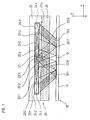
- FIG. 1 is a schematic representation of an optical position measuring device shown in addition to the scanning unit 20 according to the invention the scale 10 scanned therewith.
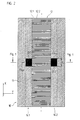
- the scale 10 used is in a plan view in FIG FIG. 2 shown.
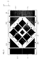
- FIG. 3 shows a detailed view of the detector plane of the scanning unit 20.
- the scanning unit 20 and the scale 10 are arranged in the specified measuring direction x relative to each other displaceable; the measuring direction x is thus in FIG. 1 oriented perpendicular to the plane of the drawing.
- the illustrated embodiment of the optical position measuring device is used for detecting linear relative movements of the scanning unit 20 and scale 10.
- a correspondingly formed position measuring device and can be used for example in a numerically controlled machine tool.
- the various position-dependent scanning signals generated by the position measuring device are hereby transmitted for further processing to an evaluation unit, not shown, for example to a numerical machine tool control.
- the scanning unit 20 can of course also be used in measuring arrangements for detecting rotary relative movements.
- the scanned scale 10 is in the embodiment of Figures 1 - 3 from a carrier body 11, on the center of which an incremental graduation track 12 is arranged in the measuring direction x.
- the incremental graduation track 12 periodically arranged reflective subareas 12.1 and non-reflective subareas 12.2, whose longitudinal axes are respectively oriented in the indicated y-direction, ie perpendicular to the measuring direction x, extend in the measuring direction x.
- a carrier body 11 can serve as a metal strip on which in the region of the incremental graduation track 12, the partial areas 12.1, 12.2 are formed with the corresponding optical properties.
- the material design of the scale 10 is not essential to the invention, i.
- the scale 10 can in principle also be realized as an alternative to the specified embodiment.
- two further reference markings 13.1, 13.2 are arranged at a reference position x REF in two reference marking tracks 14.1, 14.2.
- a definite absolute position along the measuring path is thus defined, via which the absolute reference of the high-resolution incremental measurement can be produced in a known manner.
- reference marks 13.1, 13.2 can also be attached in pairs to corresponding reference positions x REF of the scale 10 at further locations of the reference marking tracks 14.1, 14.2. It is also possible, for example, to provide so-called distance-coded reference markings and to scan them in accordance with the invention.
- the reference marks 13.1, 13.2 are formed in this example as non-reflecting regions on the otherwise reflective carrier body 12. In connection with the various optical properties of the partial regions 12.1, 12.2 in the incremental graduation track 12 or the reference markings 13.1, 13.2 in the reference marking tracks 14.1, 14.2, it should be emphasized at this point that, of course, a design as specified above does not necessarily have to be performed. It may be sufficient, for example, in the incremental graduation track 12, subregions 12.1, 12.2 alternately form with different high reflectivity. Likewise, the reference marks 13.1, 13.2 could be designed to be highly reflective in the reference marking tracks 14.1, 14.2, while the adjacent areas of the carrier body surface have only a low reflective effect, etc.
- FIG. 1 shows a view of the detector plane in the scanning unit 20.
- the scanning unit 20 comprises a centrally arranged light source 21, for example a suitable LED.
- the light source 21 serves both to illuminate the incremental graduation track 12 on the scale 10 as well as to illuminate the reference marks 13.1, 13.2 on the same.
- the incremental signal sampling arrangement comprises the scanning unit 20 a total of eight separate, each square-shaped incremental signal detector elements 22.1 - 22.8.
- Incremental signal detector elements 22.1 - 22.8 are arranged in relation to one another in such a way that partial incremental signals out of phase with the incremental graduation track 12 result on the scale 10 from the various incremental signal detector elements 22.1 - 22.8.
- the relative phase angles of the sub-incremental signals from the various incremental-signal detector elements 22.1 to 22.8 are shown in FIG. 3 respectively indicated.
- push-pull connection of the corresponding detector elements can be produced in a known manner a pair of 90 ° out of phase, sinusoidal or cosine-shaped incremental signals. Further, at this point, the known manner of generating the incremental signal did not enter; In this connection, reference is made to the abovementioned publication by R. Burgschat and the DE 195 27 287 A1 directed.
- the inventive scanning unit of the embodiment shown now comprises a total of four reference pulse detector elements 24.1 - 24.4.
- One pair each of the reference pulse detector elements 24.1 - 24.4 serves for scanning one of the two reference marks 13.1, 13.2 or reference marking tracks 14.1, 14.2 on the scale 10.
- the two in FIG. 3 on the left arranged reference pulse detector elements 24.1, 24.2 are used for scanning the in FIG. 1 on the left arranged reference marking track 14.1
- the two in FIG. 3 on the right arranged reference pulse detector elements 24.3, 24.4 are used to scan the in FIG. 1 used on the right reference mark track 14.2.
- the four reference pulse detector elements 24.1 - 24.4 are all formed identically rectangular in the illustrated embodiment, the rectangular longitudinal axes are each oriented in the measuring direction x. in principle Of course, another geometry of the reference pulse detector elements can also be selected.
- the two reference pulse detector elements 24.1 and 24.2 or 24.3 and 24.4 respectively provided for scanning a reference mark 13.1, 13.2 are arranged offset in the measuring direction x, so that two phase-shifted partial reference pulse signals result when scanning the respective reference mark 13.1, 13.2.
- the various optoelectronic components such as light source and detector elements are all arranged in the scanning unit 20 on one side of a carrier body 25.
- the components arranged glass plate 26 the components are protected against mechanical damage during measurement.
- a total of four compensating detector elements 23.1-23.4 are provided on the scanning unit 20 side.
- the compensation detector elements 23.1-23.4 each have the shape of an isosceles triangle and are arranged between the arrangement with the incremental signal detector elements 21.1-21.8 and the reference pulse detector elements 24.1-24.2. All compensation detector elements 23.1 - 23.4 are as in FIG. 3 recognizable serially interconnected.
- the compensation detector elements 23.1 - 23.4 are acted upon by reflected light from the area of the incremental graduation track 12 during the measuring operation. Due to the relatively large spatial extent of the compensation detector elements 23.1 - 23.4 in the measuring direction x and the muffled serial interconnection thereof results in the sampling of the incremental graduation track 12 from a compensation signal with largely constant signal level. To use the compensation signal in the generation of the output reference pulse signal is again to the following description of possible circuit arrangements in the FIGS. 4a and 4b directed.
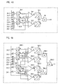
- FIG. 4a shows a first embodiment of a circuit arrangement with which a generation of an output reference pulse signal H via the scanning unit described above is possible.
- the partial reference pulse signals detected via the two reference pulse detector elements 24.3, 24.2 reach a first current-voltage converter 30.1; the partial reference pulse signals detected via the two reference pulse detector elements 24.4, 24.1 are applied to a second current-voltage converter 30.2.
- reference pulse detector elements 24.1 - 24.4 are connected in series to the input of a current-voltage converter 30.1, 30.2, which lie directly opposite one another in the scanning unit perpendicular to the measuring direction x.
- the partial compensation signals detected via the four serially interconnected compensation detector elements 23.1 - 23.4 reach a third current-voltage converter 30.3.
- the compensation signal C with almost constant signal level, which is also in FIG. 5a is shown.
- the difference and the sum of the two analog signals A and B are subsequently formed by suitably connected operational amplifiers 31.1, 31.2.
- the first operational amplifier 31.1 then lies with the signal D to the corresponding difference signal from the two signals A and B;
- the sum signal E results from the two signals A and B.
- the signals D and E thus generated are in FIG. 5b shown.
- the signals F and G are supplied to a link stage 33, which performs a logical AND operation between these signals.
- This embodiment of a possible circuit arrangement for generating an output reference pulse signal is now particularly simple in construction and comprises only a few electronic components.
- a separate processing of the partial reference pulse signals of those reference pulse detector elements which are each arranged on one side of the scanning unit and provided for scanning a reference mark on the scale now takes place.
- a first processing channel is provided in the circuit arrangement shown, in which the partial reference pulse signals of the two reference pulse detector elements 24.3, 24.4 are processed, which result from the scanning of the first reference mark 13.1; in a second processing channel, the partial reference pulse signals of the two reference pulse detector elements 24.1, 24.2 are processed, resulting from the scanning of the second reference mark 13.2. Accordingly, only the partial reference pulse signals from detector elements resulting from the scanning of the same reference mark on the scale are processed per processing channel.
- the partial reference pulse signals generated via the four reference pulse detector elements 24.1 - 24.4 are now each one of the four provided current-voltage converter 300.1 - 300.4 fed.
- the two signals A, B, in FIG. 5a are shown.
- the partial reference pulse signals from the reference pulse detector elements 24.11 24.2 are supplied to the two current-voltage converters 300.4, 300.5 in the second processing channel.
- the signals A, B, which in Fig. 5a are shown.
- the sum and the difference of the signals A and B are then formed by means of the compensation signal C.
- the signals D and E are again in FIG. 5b shown. Accordingly, the processing of the signals A and B in the second processing channel, in which then the difference signal D and the sum signal E is applied to the outputs of the two enrovend operational amplifier 310.3, 310.4.
- each of the two processing channels then takes place via a logic element 330.1, 330.2 the logical AND operation of the two Signals F and G.
- the repeated logical AND operation of the two signals H from the two processing channels with the aid of a third logic element 330.3 finally generates the desired output reference pulse signal H '.
- the output reference pulse signal H 'in this case is identical to the signals H in the two processing channels in the case of correct detection of partial reference pulse signals on both sides of the incremental track.
- FIG. 4b shown circuit arrangement offers over the in FIG. 4a explained first circuit arrangement a further advantage.
- this is due to the separate processing of the signals from the reference marks on both sides of the incremental track ensures that about no possible contamination on one side results in no erroneous generation of a reference pulse signal. This is ultimately ensured by the final logical AND operation of the two signals H from the two processing channels via the logic element 330.3.
- this variant ensures that even with a possible rotation of the scanning unit relative to the scale, the phase position of the generated output reference pulse signal H 'is maintained relative to the incremental signals. This is due to the fact that the phase position of the respective signals H from the opposing adjacent areas in such a case gegensinning each other changes. On the other hand, due to the logical AND operation on the output side, the phase position of the resulting output reference pulse signal H 'is retained; only the width of the corresponding rectangular pulse H 'changes in this case.
- the components provided in the two circuit arrangements 4a and 4b for processing the partial reference pulse signals generated by the reference pulse detector elements are also preferably all arranged on the side of the scanning unit. This can be done, for example, on the carrier body 25, on which the remaining optoelectronic components are arranged.
- the sampling unit according to the invention then supplies, in addition to the incremental signals, the output reference pulse signal H, H ', which can be further processed in the downstream evaluation unit.
Abstract
Description
Die vorliegende Erfindung betrifft eine Abtasteinheit für eine optische Positionsmeßeinrichtung. Die Abtasteinheit ist hierbei neben der Erzeugung von Inkrementalsignalen insbesondere auch für die Erzeugung von Referenzimpulssignalen geeignet.The present invention relates to a scanning unit for an optical position measuring device. The scanning unit is suitable here in addition to the generation of incremental signals in particular for the generation of reference pulse signals.
Bekannte inkrementale Positionsmeßeinrichtungen bieten neben der Erzeugung positionsabhängiger Inkementalsignale zumeist auch die Möglichkeit, an ein oder mehreren definierten Stellen entlang der Meßstrecke sogenannte Referenzimpulssignale zu erzeugen. Mit Hilfe der Referenzimpulssignale kann dann in bekannter Art und Weise ein Absolutbezug bei der Positionsmessung hergestellt werden.Known incremental Positionmeßeinrichtungen in addition to the production of position-dependent Inkementalsignale usually also have the ability to generate so-called reference pulse signals at one or more defined points along the measuring path. With the help of the reference pulse signals, an absolute reference can then be produced in the position measurement in a known manner.
Auch die in der Veröffentlichung
Bei einer derartigen Erzeugung des Referenzimpulssignales können nunmehr unter bestimmten Umständen Fehlmessungen resultieren. So ist es möglich, daß beispielsweise eine lokale Verschmutzung des Maßstabes im Bereich der Referenzmarkierungsspur zur Erzeugung eines Referenzimpulssignales führt. Desweiteren ist im Fall der Dejustage von Abtasteinheit und Maßstab um eine Achse senkrecht zur Maßstabebene keine ortsinvariante Lage des Referenzimpulssignales in Bezug auf die Inkrementalsignale mehr gewährleistet.Also in the publication
With such a generation of the reference pulse signal, erroneous measurements may now result under certain circumstances. It is thus possible, for example, for a local soiling of the scale in the region of the reference marking track to produce a reference pulse signal. Furthermore, in the case of misalignment of the scanning unit and scale about an axis perpendicular to the scale plane, no position-invariant position of the reference pulse signal with respect to the incremental signals is more ensured.
Aufgabe der vorliegenden Erfindung ist es daher, eine Abtasteinheit für eine optische Positiansmeßeinrichtung anzugeben, bei der die oben angesprochenen Probleme im Zusammenhang mit der Erzeugung von Referenzimpulssignalen möglichst vermieden werden. Darüberhinaus ist ein kompakter Aufbau der entsprechenden Abtasteinheit wünschenswert.The object of the present invention is therefore to provide a scanning unit for an optical Positiansmeßeinrichtung, in which the above-mentioned problems in connection with the generation of reference pulse signals are avoided as possible. Moreover, a compact construction of the corresponding scanning unit is desirable.
Diese Aufgabe wird gelöst durch eine Abtasteinheit mit den Merkmalen des Anspruches 1.This object is achieved by a scanning unit having the features of
Vorteilhafte Ausführungsformen der erfindungsgemäßen Abtasteinheit ergeben sich aus den Maßnahmen, die in den abhängigen Patentansprüchen aufgeführt sind.Advantageous embodiments of the scanning unit according to the invention will become apparent from the measures listed in the dependent claims.
Gegenstand des Anspruches 16 ist ferner eine optische Positionsmeßeinrichtung, die eine erfindungsgemäß aufgebaute Abtasteinheit umfaßt.The subject of claim 16 is further an optical position measuring device comprising a scanning unit constructed according to the invention.
Die erfindungsgemäßen Maßnahmen stellen nunmehr sicher, daß eine eventuelle Verdrehung der Abtasteinheit gegenüber dem Maßstab um eine Achse, die senkrecht zur Maßstabebene orientiert ist, nicht zu einer fehlerhaften Bestimmung der Referenzposition führt. Es ist vielmehr auch in diesem Fall die stabile Phasenlage des erzeugten Referenzimpulssignales in Bezug auf die Inkrementalsignale gewährleistet.The measures according to the invention now ensure that a possible rotation of the scanning unit relative to the scale by one Axis, which is oriented perpendicular to the scale level, does not lead to an erroneous determination of the reference position. Rather, in this case too, the stable phase position of the generated reference pulse signal with respect to the incremental signals is ensured.
Desweiteren liegt aufgrund der erfindungsgemäßen Erzeugung des Referenzimpulssignales eine deutlich vergrößerte Verschmutzungsunempfindlichkeit vor. Während bei einem System mit lediglich einseitig benachbart zur Inkrementalteilungsspur angeordneten Referenzmarkierungen eine lokale Verschmutzung in diesem Bereich zur fehlerhaften Erzeugung eines Referenzimpulssignales führen kann, ist bei Verwendung der erfindungsgemäßen Abtasteinheit kein Ausgangs-Referenzimpulssignal aufgrund einer eventuellen Verschmutzung des Maßstabes erzeugbar. Grund hierfür ist die Tatsache, daß erfindungsgemäß zwei Referenzmarkierungsspuren benachbart zur Inkrementalteilungsspur abgetastet werden; lediglich im Fall der tatsächlichen Detektion von Teil-Referenzimpulssignalen in beiden Referenzmarkierungsspuren resultiert überhaupt ein Ausgangs-Referenzimpulssignal.Furthermore, due to the generation according to the invention of the reference pulse signal, a significantly increased resistance to soiling is present. While in a system with only one side adjacent to the incremental graduation track arranged reference marks a local pollution in this area can lead to erroneous generation of a reference pulse signal, when using the scanning unit according to the invention no output reference pulse signal due to a possible contamination of the scale can be generated. The reason for this is the fact that according to the invention two reference mark tracks are scanned adjacent to the incremental pitch track; only in the case of the actual detection of partial reference pulse signals in both reference marker tracks does an output reference pulse signal ever result.
Darüberhinaus ist aufzuführen, daß nunmehr sowohl für die Abtastung der Inkrementalteilungspur als auch für die Abtastung der Referenzmarkierungen auf dem Maßstab lediglich eine einzige Lichtquelle erforderlich ist. Demgegenüber erforderte die in oben genannter Veröffentlichung beschriebene Variante der Abtasteinheit noch zwei separate Lichtquellen.In addition, it should be noted that now only a single light source is required for both the scanning of the incremental pitch track and the scanning of the reference marks on the scale. In contrast, the variant of the scanning unit described in the publication mentioned above required two separate light sources.
Ingesamt ergibt sich aufgrund der erfindungsgemäßen Manahmen somit eine äußerst kompakt bauende Abtasteinheit für eine optische Positionsmeßeinrichtung, die auch unter beengten Einbaubedingungen eingesetzt werden kann.Overall, due to the measures according to the invention thus results in a very compact scoring unit for an optical position measuring device that can be used even in confined installation conditions.
Selbstverständlich ist es möglich, die erfindungsgemäße Abtasteinheit sowohl in linearen wie auch in rotatorischen Positionsmeßeinrichtungen zu verwenden.Of course, it is possible to use the scanning unit according to the invention in both linear and rotational position measuring devices.
Weitere Vorteile sowie Einzelheiten der erfindungsgemäßen Abtasteinheit ergeben sich aus der nachfolgenden Beschreibung eines Ausführungsbeispieles der erfindungsgemäßen Abtasteinheit sowie mehrerer Auswerte-Schaltungsanordnungen anhand der beiliegenden Zeichnungen.Further advantages and details of the scanning unit according to the invention will become apparent from the following description of an embodiment of the scanning unit according to the invention and several evaluation circuit arrangements with reference to the accompanying drawings.
Dabei zeigt
Figur 1- eine schematische Darstellung eines Ausführungsbeispieles der erfindungsgemäßen Abtasteinheit in Verbindung mit einem abgetasteten Maßstab;
- Figur 2
- eine Draufsicht auf den abgetasteten Maßstab aus
Figur 1 - Figur 3
- eine Draufsicht auf die Detektorebene der erfindungsgemäßen Abtasteinheit aus
Figur 1 - Figur 4a
- ein Blockschaltbild einer ersten Schaltungsanordnung zur Erzeugung des Ausgangs-Referenzimpulssignales aus den erfaßten Signalen;
- Figur 4b
- ein Blockschaltbild einer zweiten Schaltungsanordnung zur Erzeugung des Ausgangs-Referenzimpulssignales aus den erfaßten Signalen;
- Figur 5a - 5d
- verschiedene Darstellungen von Signalen innerhalb der Blockschaltbilder aus den
Figuren 4a und 4b , anhand der die erfindungsgemäße Erzeugung von Ausgangs-Referenzimpulssignalen erläutert wird.
- FIG. 1
- a schematic representation of an embodiment of the scanning unit according to the invention in conjunction with a scanned scale;
- FIG. 2
- a plan view of the scanned scale
FIG. 1 ; - FIG. 3
- a plan view of the detector plane of the scanning unit according to the invention
FIG. 1 ; - FIG. 4a
- a block diagram of a first circuit arrangement for generating the output reference pulse signal from the detected signals;
- FIG. 4b
- a block diagram of a second circuit arrangement for generating the output reference pulse signal from the detected signals;
- Figure 5a - 5d
- various representations of signals within the block diagrams from the
FIGS. 4a and 4b , with reference to which the generation of output reference pulse signals according to the invention will be explained.
In
Die Abtasteinheit 20 und der Maßstab 10 sind in der angegebenen Meßrichtung x relativ zueinander verschiebbar angeordnet; die Meßrichtung x ist damit in
Das dargestellte Ausführungsbeispiel der optischen Positionsmeßeinrichtung dient zur Erfassung linearer Relativbewegungen von Abtasteinheit 20 und Maßstab 10. Eine entsprechend ausgebildete Positionsmeßeinrichtung und kann etwa in einer numerisch gesteuerten Werkzeugmaschine eingesetzt werden. Die von der Positionsmeßeinrichtung erzeugten, diversen positionsabhängigen Abtastsignale werden hierbei zur Weiterverarbeitung an eine nicht dargestellte Auswerteeinheit übertragen, beispielsweise an eine numerische Werkzeugmaschinensteuerung.The illustrated embodiment of the optical position measuring device is used for detecting linear relative movements of the
Alternativ zur dargestellten Linear-Variante kann die erfindungsgemäße Abtasteinheit 20 selbstverständlich auch in Meßanordnungen zur Erfassung rotatorischer Relativbewegungen eingesetzt werden.As an alternative to the illustrated linear variant, the
Der abgetastete Maßstab 10 besteht im Ausführungsbeispiel der
Die materialmäßige Ausbildung des Maßstabes 10 ist hierbei nicht erfindungswesentlich, d.h. der Maßstab 10 kann grundsätzlich auch alternativ zur angegebenen Ausführungsform realisiert werden.The material design of the
Seitlich benachbart zur Inkrementalteilungsspur 12 sind im gezeigten Beispiel desweiteren zwei Referenzmarkierungen 13.1, 13.2 an einer Referenzposition xREF in zwei Referenzmarkierungsspuren 14.1, 14.2 angeordnet. Mit Hilfe der Referenzmarkierungen 13.1, 13.2 wird somit eine eindeutige Absolutposition entlang der Meßstrecke definiert, über die der Absolutbezug der hochauflösenden Inkrementalmessung in bekannter Art und Weise hergestellt werden kann.Laterally adjacent to the
Selbstverständlich können auch noch an weiteren Stellen der Referenzmarkierungsspuren 14.1, 14.2 derartige Referenzmarkierungen 13.1, 13.2 paarweise an entsprechenden Referenzpositionen xREF des Maßstabes 10 angebracht werden. Ebenso ist es möglich, etwa auch sogenannte abstandscodierte Referenzmarkierungen vorzusehen und erfindungsgemäß abzutasten etc..Of course, such reference marks 13.1, 13.2 can also be attached in pairs to corresponding reference positions x REF of the
Im Ausführungsbeispiel der
Die Referenzmarkierungen 13.1, 13.2 sind in diesem Beispiel als nicht-reflektierende Bereiche auf dem ansonsten reflektierenden Trägerkörper 12 ausgebildet.
Im Zusammenhang mit den verschiedenen optischen Eigenschaften der Teilbereiche 12.1, 12.2 in der Inkrementalteilungsspur 12 bzw. der Referenzmarkierungen 13.1, 13.2 in den Referenzmarkierungsspuren 14.1, 14.2 sei an dieser Stelle betont, daß eine wie oben spezifizierte Auslegung selbstverständlich nicht zwingend erfolgen muß. Es kann beispielsweise in der Inkrementalteilungsspur 12 ausreichen, Teilbereiche 12.1, 12.2 alternierend mit unterschiedlich hoher Reflektivität auszubilden. Ebenso könnten die Referenzmarkierungen 13.1, 13.2 in den Referenzmarkierungsspuren 14.1, 14.2 hoch reflektierend ausgelegt werden, während die angrenzenden Bereiche der Trägerkörper-Oberfläche lediglich gering reflektierend wirken etc..The reference marks 13.1, 13.2 are formed in this example as non-reflecting regions on the otherwise
In connection with the various optical properties of the partial regions 12.1, 12.2 in the
Wie bereits oben angedeutet bietet eine derartige Anordnung von zwei Referenzmarkierungen 13.1, 13.2 seitlich benachbart zur Inkrementalteilungsspur 12 deutliche Vorteile gegenüber der lediglich einseitigen Anordnung einer Referenzmarkierung. So ist damit praktisch ausgeschlossen, daß etwa eine lokale Verschmutzung, die ebenfalls optisch reflexmindernd wirkt und sich benachbart zur Inkrementalteilungsspur 12 befindet, als Referenzmarkierung interpretiert werden kann. Dies wird durch die nachfolgend noch detailliert zu erläuternde Verarbeitung der resultierenden Abtastsignale aus beiden Referenzmarkierungen 13.1, 13.2 sichergestellt.
Ferner ist auch im Fall einer Verdrehung der Abtasteinheit 20 gegenüber dem Maßstab 10 um die z-Achse sichergestellt, daß die Phasenlage des letztlich erzeugten Ausgangs-Referenzimpulssignales sich gegenüber den Inkrementalsignalen nicht unerwünscht verändert.As already indicated above, such an arrangement of two reference markings 13.1, 13.2 laterally adjacent to the
Furthermore, even in the case of a rotation of the
Auf Seiten der erfindungsgemäßen Abtasteinheit 20 sind in der schematischen Darstellung der
Die erfindungsgemäße Abtasteinheit 20 umfaßt eine zentral angeordnete Lichtquelle 21, beispielsweise eine geeignete LED. Die Lichtquelle 21 dient hierbei sowohl zur Beleuchtung der Inkrementalteilungsspur 12 auf dem Maßstab 10 wie auch zur Beleuchtung der Referenzmarkierungen 13.1, 13.2 auf demselben. Symmetrisch um die Lichtquelle 21 ist eine Anordnung aus mehreren Inkrementalsignal-Detektorelementen 22.1 ― 22.8 vorgesehen, die nachfolgend kurz als Inkrementalsignal-Abtastanordnung bezeichnet sei. Im dargestellten Ausführungsbeispiel umfaßt die Inkrementalsignal-Abtastanordnung der Abtasteinheit 20 insgesamt acht separate, jeweils quadratisch ausgebildete Inkrementalsignal-Detektorelemente 22.1 ― 22.8. Die Inkrementalsignal-Detektorelemente 22.1 ― 22.8 sind hierbei derart zueinander angeordnet, daß bei der entsprechenden Auflicht-Abtastung der Inkrementalteilungsspur 12 auf dem Maßstab 10 phasenversetzte Teil-Inkrementalsignale aus den verschiedenen Inkrementalsignal-Detektorelementen 22.1 ― 22.8 resultieren. Die relativen Phasenlagen der Teil-Inkrementalsignale aus den verschiedenen Inkrementalsignal-Detektorelementen 22.1 ― 22.8 sind in
Weiter sei an dieser Stelle auf die bekannte Art und Weise der Inkrementalsignal-Erzeugung nicht eingegegangen; es wird in diesem Zusammenhang auf die oben erwähnte Publikation von R. Burgschat sowie die
Further, at this point, the known manner of generating the incremental signal did not enter; In this connection, reference is made to the abovementioned publication by R. Burgschat and the
Zur photoelektrischen Abtastung der benachbart zur Inkrementalteilungsspur 12 angeordneten Referenzmarkierungen 13.1, 13.2 auf dem Maßstab 10 umfaßt die erfindungsgemäße Abtasteinheit des gezeigten Ausführungsbeispiels nunmehr ingesamt vier Referenzimpuls-Detektorelemente 24.1 ― 24.4. Je ein Paar der Referenzimpuls-Detektorelemente 24.1 ― 24.4 dient hierbei zur Abtastung einer der beiden Referenzmarkierungen 13.1, 13.2 bzw. Referenzmarkierungsspuren 14.1, 14.2 auf dem Maßstab 10. Die beiden in
Die vier Referenzimpuls-Detektorelemente 24.1 ― 24.4 sind im dargestellten Ausführungsbeispiel allesamt identisch rechteckförmig ausgebildet, wobei die Rechteckslängsachsen jeweils in Meßrichtung x orientiert sind. Grundsätzlich kann selbstverständlich auch eine andere Geometrie der Referenzimpuls-Detektorelemente gewählt werden.The four reference pulse detector elements 24.1 - 24.4 are all formed identically rectangular in the illustrated embodiment, the rectangular longitudinal axes are each oriented in the measuring direction x. in principle Of course, another geometry of the reference pulse detector elements can also be selected.
Die zur Abtastung einer Referenzmarkierung 13.1, 13.2 jeweils vorgesehenen zwei Referenzimpuls-Detektorelemente 24.1 und 24.2 bzw. 24.3 und 24.4 sind in Meßrichtung x versetzt zueinander angeordnet, so daß bei der Abtastung der jeweiligen Referenzmarkierung 13.1, 13.2 zwei phasenversetzte Teil-Referenzimpulssignale resultieren. Der Abstand der beiden derart erzeugten Teil-Referenzimpulssignale beträgt in der gezeigten Ausführungsform in Meßrichtung x dabei etwa 0.5mm, was bei einer Teilungsperiode der Inkrementalteilungsspur von TP = 20µm dann entsprechend 25 Signalperioden des Inkrementalsignales ausmacht.The two reference pulse detector elements 24.1 and 24.2 or 24.3 and 24.4 respectively provided for scanning a reference mark 13.1, 13.2 are arranged offset in the measuring direction x, so that two phase-shifted partial reference pulse signals result when scanning the respective reference mark 13.1, 13.2. The distance between the two partial reference pulse signals thus generated is approximately 0.5 mm in the embodiment shown in the measuring direction x, which then corresponds to 25 signal periods of the incremental signal in the case of a graduation period of the incremental graduation track of TP = 20 μm.
Die verschiedenen optoelektronischen Bauelemente wie Lichtquelle und Detektorelemente sind in der Abtasteinheit 20 allesamt auf einer Seite eines Trägerkörpers 25 angeordnet. Über eine oberhalb der Bauelemente angeordnete Glasplatte 26 werden die Bauelemente gegen mechanische Beschädigung im Meßbetrieb geschützt.The various optoelectronic components such as light source and detector elements are all arranged in the
Im Zusammenhang mit der Verarbeitung der Signale und der Erzeugung des letztlich an die Auswerteeinheit zu übertragenden Ausgangs-Referenzimpulssignales sei an dieser Stelle auf die nachfolgende Beschreibung der Schaltungsanordnungen in den
Für die Weiterverarbeitung der Teil-Referenzimpulssignale als auch für die Verarbeitung der erzeugten Teil-Inkrementalsignale sind auf Seiten der Abtasteinheit 20 ferner ingesamt vier Kompensations-Detektorelemente 23.1 ― 23.4 vorgesehen. Die Kompensations-Detektorelemente 23.1 ― 23.4 weisen in dieser Ausführungsform jeweils die Form eines gleichschenkligen Dreieckes auf und sind zwischen der Anordnung mit den Inkrementalsignal-Detektorelementen 21.1 - 21.8 und den Referenzimpuls-Detektorelementen 24.1 ― 24.2 angeordnet. Sämtliche Kompensations-Detektorelemente 23.1 ― 23.4 sind wie in
Es ergibt sich aufgrund der gewählten Anordnung der verschiedenen Detektorelemente somit eine äußerst kompakte Ausgestaltung der Abtasteinheit 20. Gleichzeitig stehen aber detektorseitig hinreichend große Flächen zur Detektion der verschiedenen Abtastsignale zur Verfügung.Due to the selected arrangement of the various detector elements, this results in an extremely compact embodiment of the
Die Kompensations-Detektorelemente 23.1 ― 23.4 werden im Meßbetrieb von reflektiertem Licht aus dem Bereich der Inkrementalteilungsspur 12 beaufschlagt. Aufgrund der relativ großen räumlichen Ausdehnung der Kompensations-Detektorelemente 23.1 ― 23.4 in Meßrichtung x und der gewühlten seriellen Verschaltung derselben resultiert bei der Abtastung der Inkrementalteilungsspur 12 daraus ein Kompensationssignal mit weitestgehend gleichbleibendem Signalpegel. Zur Nutzung des Kompensationssignales bei der Erzeugung des Ausgangs-Referenzimpulssignales sei wiederum auf die nachfolgende Beschreibung möglicher Schaltungsanordnungen in den
In der Auswertungs-Variante gemäß
Es werden demzufolge jeweils diejenigen Referenzimpuls-Detektorelemente 24.1 ― 24.4 seriell auf den Eingang eines Strom-Spannungs-Wandlers 30.1, 30.2 geschaltet, die sich in der Abtasteinheit senkrecht zur Meßrichtung x direkt gegenüberliegen.Accordingly, in each case those reference pulse detector elements 24.1 - 24.4 are connected in series to the input of a current-voltage converter 30.1, 30.2, which lie directly opposite one another in the scanning unit perpendicular to the measuring direction x.
Die über die vier seriell verschalteten Kompensations-Detektorelemente 23.1 - 23.4 detektierten Teil-Kompensationssignale wiederum gelangen auf einen dritten Strom-Spannungs-Wandler 30.3. An dessen Ausgang resultiert dann das Kompensationssignal C mit nahezu gleichbleibendem Signalpegel, welches ebenfalls in
Aus den Signalen A, B und C wird nachfolgend durch geeignet beschaltete Operationsverstärker 31.1, 31.2 die Differenz und die Summe aus den beiden analogen Signalen A und B gebildet. Am Ausgang des ersten Operationsverstärkers 31.1 liegt dann mit dem Signal D das entsprechende Differenzsignal aus den beiden Signalen A und B an; am Ausgang des zweiten Operationsverstärkers 31.2 resultiert das Summensignal E aus den beiden Signalen A und B. Die derart generierten Signale D und E sind in
Aus den beiden Signalen D und E werden anschließend über die beiden Fensterkomparatoren 32.1, 32.2 entsprechende rechteckförmige Signale F und G erzeugt, die in
Daraufhin werden die Signale F und G einer Verknüpfungsstufe 33 zugeführt, die eine logische UND-Verknüpfung zwischen diesen Signalen durchführt. Nach der entsprechenden UND-Verknüpfung liegt dann am Ausgang der Verknüpfungsstufe 33 schließlich an der Referenzposition xREF = 0 das gewünschte Ausgangs-Referenzimpulssignal H an, welches wiederum in
Diese Ausführungsform einer möglichen Schaltungsanordnung zur Erzeugung eines Ausgangs-Referenzimpulssignales ist nunmehr insbesondere einfach aufgebaut und umfaßt nur wenige Elektronik-Komponenten.This embodiment of a possible circuit arrangement for generating an output reference pulse signal is now particularly simple in construction and comprises only a few electronic components.
Desweiteren ist die oben erwähnte Forderung nach Invarianz der Phasenbeziehung zwischen dem Ausgangs-Referenzimpulssignal und den Inkrementalsignalen im Fall der Verdrehung um die z-Achse gewährleistet.Furthermore, the above-mentioned requirement for invariance of the phase relationship between the output reference pulse signal and the incremental signals in the case of rotation about the z-axis is ensured.
Eine zweite Ausführungsform einer Schaltungsanordnung zur Erzeugung eines Ausgangs-Referenzimpulssignales aus den verschiedenen Signalen, die über die erfindungsgemäße Abtasteinheit detektiert werden, sei abschließend anhand von
Im Unterschied zum vorherigen Beispiel erfolgt nunmehr eine getrennte Verarbeitung der Teil-Referenzimpulsignale derjenigen Referenzimpuls-Detektorelemente, die jeweils auf einer Seite der Abtasteinheit angeordnet und zur Abtastung einer Referenzmarkierung auf dem Maßstab vorgesehen sind. Im dargestellten Beispiel ist demzufolge ein erster Verarbeitungskanal in der gezeigten Schaltungsanordnung vorgesehen, in dem die Teil-Referenzimpulssignale der beiden Referenzimpuls-Detektorelemente 24.3, 24.4 verarbeitet werden, welche aus der Abtastung der ersten Referenzmarkierung 13.1 resultieren; in einem zweiten Verarbeitungskanal werden die Teil-Referenzimpulssignale der beiden Referenzimpuls-Detektorelemente 24.1, 24.2 verarbeitet, die sich aus der Abtastung der zweiten Referenzmarkierung 13.2 ergeben. Pro Verarbeitungskanal werden demzufolge lediglich diejenigen Teil-Referenzimpulssignale von Detektorelementen verarbeitet, die aus der Abtastung der gleichen Referenzmarkierung auf dem Maßstab resultieren. Im jeweils anderen Verarbeitungskanal erfolgt die Signalverarbeitung derjenigen Teil-Referenzimpulssignale, die aus der Abtastung der gegenüberliegenden Referenzmarkierung resultieren.
Gemeinsam werden hingegen in beiden Verarbeitungskanälen die über die Kompensations-Detektorelemente 23.1 ― 23.4 erzeugten Signale genutzt. Auf die besonderen Vorteile dieser Auswerteanordnung zur Signalverarbeitung sei im Verlauf der nachfolgenden Beschreibung noch näher eingegangen.In contrast to the previous example, a separate processing of the partial reference pulse signals of those reference pulse detector elements which are each arranged on one side of the scanning unit and provided for scanning a reference mark on the scale now takes place. In the illustrated example, therefore, a first processing channel is provided in the circuit arrangement shown, in which the partial reference pulse signals of the two reference pulse detector elements 24.3, 24.4 are processed, which result from the scanning of the first reference mark 13.1; in a second processing channel, the partial reference pulse signals of the two reference pulse detector elements 24.1, 24.2 are processed, resulting from the scanning of the second reference mark 13.2. Accordingly, only the partial reference pulse signals from detector elements resulting from the scanning of the same reference mark on the scale are processed per processing channel. In the respective other processing channel, the signal processing of those partial reference pulse signals which result from the scanning of the opposite reference mark takes place.
In contrast, the signals generated via the compensation detector elements 23.1-23.4 are used in common in both processing channels. The particular advantages of this evaluation arrangement for signal processing will be discussed in more detail in the course of the following description.
Die über die vier Referenzimpuls-Detektorelemente 24.1 ― 24.4 erzeugten Teil-Referenzimpulssignale werden nunmehr jeweils einem der ebenfalls vier vorgesehenen Strom-Spannungs-Wandler 300.1 ― 300.4 zugeführt. Im ersten Verarbeitungskanal resultieren am Ausgang der Strom-Spannungswandler 300.1, 300.2 die beiden Signale A, B, die in
Auf einen weiteren Strom-Spannungs-Wandler 300.3 werden die Signale der Kompensations-Detektorelemente 23.1 ― 23.4 geschaltet; das entsprechende Kompensationssignal C am Ausgang des Strom-Spannungs-Wandlers 300.3 mit nahezu gleichbleibendem Signalpegel ist ebenfalls wieder in
In beiden Verarbeitungskanälen wird anschließend mit Hlfe des Kompensationssignales C jeweils die Summe und die Differenz aus den Signalen A und B gebildet. An den Ausgängen der entsprechend beschalteten Operationsverstärker 310.1, 310.3 des ersten Verarbeitungskanales liegt dann mit den Signalen D und E das entsprechende Differenz- und Summensignal an. Die Signale D und E sind wiederum in
Mit Hilfe nachgeordneter Fensterkomparatoren 320.1 ― 320.4 werden die Summen- und Differenzsignale E, D anschließend in entsprechende rechteckförmige Signale G und F umgewandelt, wie sie wiederum in
In jedem der beiden Verabeitungskanäle erfolgt anschließend über ein Verknüpfungselement 330.1, 330.2 die logische UND-Verknüpfung der beiden Signale F und G. Am Ausgang der Verknüpfungselemente liegt dann in beiden Verarbeitungskanälen im Bereich der Referenzposition xREF = 0 ein Signal H vor, das in
Über die nochmalige logische UND-Verknüpfung der beiden Signale H aus den zwei Verarbeitungskanälen mit Hilfe eines dritten Verknüpfungselementes 330.3 wird schließlich das gewünschte Ausgangs-Referenzimpulssignal H' erzeugt. Das Ausgangs-Referenzimpulssignal H' ist hierbei im Fall einer korrekten Detektion von Teil-Referenzimpulssignalen auf beiden Seiten der Inkrementalspur identisch mit den Signalen H in den beiden Verarbeitungskanälen.The repeated logical AND operation of the two signals H from the two processing channels with the aid of a third logic element 330.3 finally generates the desired output reference pulse signal H '. The output reference pulse signal H 'in this case is identical to the signals H in the two processing channels in the case of correct detection of partial reference pulse signals on both sides of the incremental track.
Die in
Desweiteren gewährleistet auch diese Variante, daß auch bei einer eventuellen Verdrehung der Abtasteinheit gegenüber dem Maßstab die Phasenlage des erzeugten Ausgangs-Referenzimpulssignales H' gegenüber den Inkrementalsignalen erhalten bleibt. Dies ist darauf zurückzuführen, daß sich die Phasenlage der jeweiligen Signale H aus den gegenüberliegend benachbarten Bereichen in einem derartigen Fall gegensinning zueinander ändert. Aufgrund der ausgangsseitig erfolgenden logischen UND-Verknüpfung wiederum bleibt die Phasenlage des derart resultierenden Ausgangs-Referenzimpulssignales H' jedoch erhalten; lediglich die Breite des entsprechenden Rechteckpulses H' verändert sich in diesem Fall.Furthermore, this variant ensures that even with a possible rotation of the scanning unit relative to the scale, the phase position of the generated output reference pulse signal H 'is maintained relative to the incremental signals. This is due to the fact that the phase position of the respective signals H from the opposing adjacent areas in such a case gegensinning each other changes. On the other hand, due to the logical AND operation on the output side, the phase position of the resulting output reference pulse signal H 'is retained; only the width of the corresponding rectangular pulse H 'changes in this case.
Die in den beiden Schaltungsanordnungen 4a und 4b vorgesehenen Bauelemente zur Verarbeitung der von den Referenzimpuls-Detektorelementen erzeugten Teil-Referenzimpulssignale sind vorzugsweise ebenfalls allesamt auf Seiten der Abtasteinheit angeordnet. Dies kann beispielsweise auf dem Trägerkörper 25 erfolgen, auf dem auch die restlichen optoelektronischen Bauelemente angeordnet werden. Ausgangsseitig liefert die erfindungsgemäße Abtasteinheit dann neben den Inkrementalsignalen das Ausgangs-Referenzimpulssignal H, H', das in der nachgeordneten Auswerteeinheit weiterverarbeitet werden kann.The components provided in the two circuit arrangements 4a and 4b for processing the partial reference pulse signals generated by the reference pulse detector elements are also preferably all arranged on the side of the scanning unit. This can be done, for example, on the
Neben den erläuterten Beispielen existieren im Rahmen der vorliegenden Erfindung selbstverständlich noch eine Vielzahl weiterer Ausführungsmöglichkeiten.In addition to the illustrated examples, there are, of course, a large number of further possible embodiments in the context of the present invention.
Claims (16)
- Scanning unit for an optical position measuring device which is suitable for scanning a scale (10) in a measuring direction (x), which scale comprises at least one incremental division track (12) and also two reference markings (13.1, 13.2) at at least one defined reference position (xREF) and the scanning unit (20) comprising the following components:- a light source (21),- an incremental signal scanning arrangement which is disposed symmetrically around the light source (21) and comprises a plurality of incremental signal detector elements (22.1 - 22.8) which are disposed respectively relative to each other such that phase-offset partial incremental signals can thus be produced from scanning the incremental division track (12),- at least two reference impulse detector elements (24.1 - 24.4) which are disposed on both sides perpendicular to the measuring direction (x) and respectively adjacent to the incremental signal scanning arrangement and serve to produce an output reference impulse signal (H'), at least one of the reference impulse detector elements (24.1 - 24.4) respectively being suitable for scanning respectively one of the reference markings (13.1, 13.2).
- Scanning unit according to claim 1, at least two reference impulse detector elements (24.1 - 24.4) respectively being disposed on one side of the incremental signal scanning arrangement and a partial reference impulse signal being able to be produced via each of the at least four reference impulse detector elements (24.1 - 24.4).
- Scanning unit according to claim 1, the reference impulse detector elements (24.1 - 24.4) respectively having a rectangular configuration and the rectangular longitudinal axis being orientated in the measuring direction (x).
- Scanning unit according to claim 2, the respectively two reference impulse detector elements (24.1, 24.2; 24.3, 24.4) on one side of the incremental signal scanning arrangement being disposed at a spacing relative to each other in the measuring direction (x).
- Scanning unit according to claim 1, the scanning unit (20) comprising in addition a plurality of compensation detector elements (23.1 - 23.4) which serve to produce a compensation signal (C) with a constant signal level.
- Scanning unit according to claim 5, the compensation detector elements (23.1 - 23.4) being disposed between the incremental signal scanning arrangement and the reference impulse detector elements (24.1 - 24.4) and being connected to each other in series.
- Scanning unit according to claim 6, the scanning unit (20) comprising four compensation detector elements (23.1 - 23.4) which have respectively the shape of an equilateral triangle and all the compensation detector elements (23.1 - 23.4) being placed symmetrically around the incremental signal scanning arrangement.
- Scanning unit according to claim 1, the scanning unit (20) comprising in addition components for processing the partial reference impulse signals produced by the reference impulse detector elements (24.1 - 24.4).
- Scanning unit according to claim 8, the formation of a sum- and a difference signal (D, E) from the partial reference impulse signals being effected via the components, said partial reference impulse signals being applied at the outputs of those detector elements (24.1 - 24.4) which are disposed offset relative to each other in the measuring direction, and a logic AND operation of the sum- and difference signal being effected after conversion of the sum- and difference signals (D, E) into rectangular signals (F, G) so that the logic AND operation delivers the output reference impulse signal (H, H').
- Scanning unit according to claims 2 and 8, the scanning unit (20) comprising respectively one processing channel with a plurality of electronic components for processing those partial reference impulse signals which can be produced respectively on one side of the incremental signal scanning arrangement.
- Scanning unit according to claim 10, the partial reference impulse signals of two associated reference impulse detector elements (24.1 - 24.4) being able to be supplied to each processing channel and a reference impulse signal (H) being applied at the output of each processing channel.
- Scanning unit according to claim 11, the scanning unit (20) comprising a linking element (330.3) to which the output-side reference impulse signals (H) of each processing channel can be supplied so that the further processed output reference impulse signal (H') is applied at the output of the linking element (330.3).
- Scanning unit according to claim 12, a logic AND operation being effected via the linking element (330.3).
- Scanning unit according to claim 11, each processing channela) comprising components (310.1 - 310.4) for summation and subtraction, to which the partial reference impulse signals can be supplied,b) comprising window comparators (320.1 - 320.4) which are disposed respectively subsequent to the summation and subtraction components (310.1 - 310.4) which convert the input signals into rectangular output signals (F, G),c) comprising a linking element (330.1, 330.2) which is disposed subsequent to the window comparators (320.1 - 320.4), to which linking element the rectangular output signals (F, G) of the window comparator (320.1 - 320.4) can be supplied and via which a logic AND operation is effected.
- Scanning unit according to claim 14, a further linking element (330.3) being disposed subsequent to the two processing channels, via which a logic AND operation of the signals (H) which are applied at the output of the two processing channels is effected.
- Optical position measuring device having a scanning unit (20) according to at least one of the preceding claims.
Applications Claiming Priority (2)
| Application Number | Priority Date | Filing Date | Title |
|---|---|---|---|
| DE19921309A DE19921309A1 (en) | 1999-05-07 | 1999-05-07 | Scanning unit for an optical position measuring device |
| DE19921309 | 1999-05-07 |
Publications (3)
| Publication Number | Publication Date |
|---|---|
| EP1050742A2 EP1050742A2 (en) | 2000-11-08 |
| EP1050742A3 EP1050742A3 (en) | 2001-09-12 |
| EP1050742B1 true EP1050742B1 (en) | 2008-06-18 |
Family
ID=7907458
Family Applications (1)
| Application Number | Title | Priority Date | Filing Date |
|---|---|---|---|
| EP00107758A Expired - Lifetime EP1050742B1 (en) | 1999-05-07 | 2000-04-11 | Scanning unit for an optical position measuring device |
Country Status (4)
| Country | Link |
|---|---|
| EP (1) | EP1050742B1 (en) |
| JP (1) | JP4580060B2 (en) |
| AT (1) | ATE398762T1 (en) |
| DE (2) | DE19921309A1 (en) |
Cited By (1)
| Publication number | Priority date | Publication date | Assignee | Title |
|---|---|---|---|---|
| WO2011113666A2 (en) | 2010-03-16 | 2011-09-22 | Dr. Johannes Heidenhain Gmbh | Scanning unit for an optical position measuring device |
Families Citing this family (9)
| Publication number | Priority date | Publication date | Assignee | Title |
|---|---|---|---|---|
| DE10043828B4 (en) * | 2000-09-06 | 2016-11-10 | Dr. Johannes Heidenhain Gmbh | Scanning unit for an optical position-measuring device |
| DE10116599A1 (en) | 2001-04-03 | 2003-02-06 | Heidenhain Gmbh Dr Johannes | Optical position measuring device |
| KR100437275B1 (en) * | 2001-06-29 | 2004-06-23 | 삼성물산 주식회사 | Method for for measuring displacement of moving body formed of displacement measuring mark using line scan camera |
| JP3738742B2 (en) * | 2002-03-27 | 2006-01-25 | 富士電機ホールディングス株式会社 | Optical absolute value encoder and moving device |
| DE102007035345A1 (en) * | 2006-11-20 | 2008-05-21 | Dr. Johannes Heidenhain Gmbh | Position measuring device |
| JP5147368B2 (en) | 2006-11-20 | 2013-02-20 | ドクトル・ヨハネス・ハイデンハイン・ゲゼルシヤフト・ミツト・ベシユレンクテル・ハフツング | Encoder |
| DE102008054433B4 (en) | 2008-12-09 | 2023-09-28 | Dr. Johannes Heidenhain Gmbh | Position measuring device |
| CN102313517B (en) * | 2011-08-23 | 2013-01-09 | 广州市诺信数字测控设备有限公司 | Optical grating ruler with double light sources |
| DE102020134604B4 (en) | 2020-12-22 | 2022-07-14 | Smaract Gmbh | Device and method for position determination |
Family Cites Families (9)
| Publication number | Priority date | Publication date | Assignee | Title |
|---|---|---|---|---|
| DE3726678C1 (en) * | 1987-08-11 | 1989-03-09 | Heidenhain Gmbh Dr Johannes | Incremental length or angle measuring device |
| US4943716A (en) * | 1988-01-22 | 1990-07-24 | Mitutoyo Corporation | Diffraction-type optical encoder with improved detection signal insensitivity to optical grating gap variations |
| DE3914739A1 (en) * | 1989-05-05 | 1990-11-08 | Heidenhain Gmbh Dr Johannes | INCREMENTAL POSITION MEASURING DEVICE WITH REFERENCE BRANDS |
| DE4323712C2 (en) * | 1993-07-15 | 1997-12-11 | Heidenhain Gmbh Dr Johannes | Photoelectric length or angle measuring device |
| JP3395339B2 (en) * | 1994-03-31 | 2003-04-14 | ソニー・プレシジョン・テクノロジー株式会社 | Fixed point detector |
| JPH08327401A (en) * | 1995-05-30 | 1996-12-13 | Canon Inc | Displacement-information detection apparatus, drive control device and scale for detection of displacement information |
| DE19527287C2 (en) * | 1995-07-26 | 2000-06-29 | Heidenhain Gmbh Dr Johannes | Photoelectric path and angle measuring system for measuring the displacement of two objects to each other |
| JP3649363B2 (en) * | 1996-10-16 | 2005-05-18 | 株式会社安川電機 | Optical position detector |
| JPH10132612A (en) * | 1996-10-28 | 1998-05-22 | Mitsutoyo Corp | Optical displacement detecting device |
-
1999
- 1999-05-07 DE DE19921309A patent/DE19921309A1/en not_active Withdrawn
-
2000
- 2000-04-11 EP EP00107758A patent/EP1050742B1/en not_active Expired - Lifetime
- 2000-04-11 AT AT00107758T patent/ATE398762T1/en not_active IP Right Cessation
- 2000-04-11 DE DE50015206T patent/DE50015206D1/en not_active Expired - Lifetime
- 2000-05-01 JP JP2000132331A patent/JP4580060B2/en not_active Expired - Fee Related
Cited By (2)
| Publication number | Priority date | Publication date | Assignee | Title |
|---|---|---|---|---|
| WO2011113666A2 (en) | 2010-03-16 | 2011-09-22 | Dr. Johannes Heidenhain Gmbh | Scanning unit for an optical position measuring device |
| DE102010002902A1 (en) | 2010-03-16 | 2011-09-22 | Dr. Johannes Heidenhain Gmbh | Scanning unit for an optical position-measuring device |
Also Published As
| Publication number | Publication date |
|---|---|
| JP2000329585A (en) | 2000-11-30 |
| DE50015206D1 (en) | 2008-07-31 |
| JP4580060B2 (en) | 2010-11-10 |
| EP1050742A3 (en) | 2001-09-12 |
| EP1050742A2 (en) | 2000-11-08 |
| DE19921309A1 (en) | 2000-11-09 |
| ATE398762T1 (en) | 2008-07-15 |
Similar Documents
| Publication | Publication Date | Title |
|---|---|---|
| EP0160811B1 (en) | Photoelectric measuring device | |
| DE19833439B4 (en) | Optical position measuring device | |
| EP1111345B1 (en) | Position measuring device with incremental track with two different graduation periods | |
| EP1003012B3 (en) | Optical position measuring arrangement | |
| EP1407231B1 (en) | Position measuring device | |
| DE69930341T2 (en) | Encoder for the supply of incremental and absolute position values | |
| EP0141123B1 (en) | Light-electric incremental measurement device | |
| EP0163824A2 (en) | Photoelectric measuring device | |
| EP1995566B1 (en) | Measuring rod for a positioning system and positioning system | |
| EP0106032A2 (en) | Feeler head for two or more coordinates measurement | |
| EP1050742B1 (en) | Scanning unit for an optical position measuring device | |
| EP2063230A2 (en) | Optical positioning device | |
| EP3511680A1 (en) | Position measuring device | |
| AT410485B (en) | POSITION MEASURING DEVICE | |
| CH672679A5 (en) | ||
| EP1524503B1 (en) | Optical encoder | |
| EP0303008B1 (en) | Incremental length or angle measuring device | |
| EP2878930B1 (en) | Position measuring device | |
| EP1427985A1 (en) | Position measuring system and method for operating such a position measuring system | |
| EP1377799B1 (en) | Optical position measuring device | |
| DE10043828B4 (en) | Scanning unit for an optical position-measuring device | |
| EP0385386B1 (en) | Method and device to measure a rotation angle | |
| DE10346380B4 (en) | Position measuring device | |
| DE19936181A1 (en) | Optical position measuring device | |
| EP3936830B1 (en) | Optical positioning device |
Legal Events
| Date | Code | Title | Description |
|---|---|---|---|
| PUAI | Public reference made under article 153(3) epc to a published international application that has entered the european phase |
Free format text: ORIGINAL CODE: 0009012 |
|
| AK | Designated contracting states |
Kind code of ref document: A2 Designated state(s): AT BE CH CY DE DK ES FI FR GB GR IE IT LI LU MC NL PT SE |
|
| AX | Request for extension of the european patent |
Free format text: AL;LT;LV;MK;RO;SI |
|
| PUAL | Search report despatched |
Free format text: ORIGINAL CODE: 0009013 |
|
| AK | Designated contracting states |
Kind code of ref document: A3 Designated state(s): AT BE CH CY DE DK ES FI FR GB GR IE IT LI LU MC NL PT SE |
|
| AX | Request for extension of the european patent |
Free format text: AL;LT;LV;MK;RO;SI |
|
| RIC1 | Information provided on ipc code assigned before grant |
Free format text: 7G 01B 11/00 A, 7G 01B 11/02 B, 7G 01D 5/347 B |
|
| 17P | Request for examination filed |
Effective date: 20020312 |
|
| AKX | Designation fees paid |
Free format text: AT BE CH CY DE DK ES FI FR GB GR IE IT LI LU MC NL PT SE |
|
| GRAP | Despatch of communication of intention to grant a patent |
Free format text: ORIGINAL CODE: EPIDOSNIGR1 |
|
| GRAS | Grant fee paid |
Free format text: ORIGINAL CODE: EPIDOSNIGR3 |
|
| GRAA | (expected) grant |
Free format text: ORIGINAL CODE: 0009210 |
|
| AK | Designated contracting states |
Kind code of ref document: B1 Designated state(s): AT BE CH CY DE DK ES FI FR GB GR IE IT LI LU MC NL PT SE |
|
| REG | Reference to a national code |
Ref country code: GB Ref legal event code: FG4D Free format text: NOT ENGLISH |
|
| REF | Corresponds to: |
Ref document number: 50015206 Country of ref document: DE Date of ref document: 20080731 Kind code of ref document: P |
|
| REG | Reference to a national code |
Ref country code: CH Ref legal event code: EP Ref country code: CH Ref legal event code: NV Representative=s name: TROESCH SCHEIDEGGER WERNER AG |
|
| REG | Reference to a national code |
Ref country code: IE Ref legal event code: FG4D Free format text: LANGUAGE OF EP DOCUMENT: GERMAN |
|
| PG25 | Lapsed in a contracting state [announced via postgrant information from national office to epo] |
Ref country code: FI Free format text: LAPSE BECAUSE OF FAILURE TO SUBMIT A TRANSLATION OF THE DESCRIPTION OR TO PAY THE FEE WITHIN THE PRESCRIBED TIME-LIMIT Effective date: 20080618 |
|
| PG25 | Lapsed in a contracting state [announced via postgrant information from national office to epo] |
Ref country code: NL Free format text: LAPSE BECAUSE OF FAILURE TO SUBMIT A TRANSLATION OF THE DESCRIPTION OR TO PAY THE FEE WITHIN THE PRESCRIBED TIME-LIMIT Effective date: 20080618 |
|
| NLV1 | Nl: lapsed or annulled due to failure to fulfill the requirements of art. 29p and 29m of the patents act | ||
| PG25 | Lapsed in a contracting state [announced via postgrant information from national office to epo] |
Ref country code: PT Free format text: LAPSE BECAUSE OF FAILURE TO SUBMIT A TRANSLATION OF THE DESCRIPTION OR TO PAY THE FEE WITHIN THE PRESCRIBED TIME-LIMIT Effective date: 20081118 Ref country code: ES Free format text: LAPSE BECAUSE OF FAILURE TO SUBMIT A TRANSLATION OF THE DESCRIPTION OR TO PAY THE FEE WITHIN THE PRESCRIBED TIME-LIMIT Effective date: 20080929 Ref country code: SE Free format text: LAPSE BECAUSE OF FAILURE TO SUBMIT A TRANSLATION OF THE DESCRIPTION OR TO PAY THE FEE WITHIN THE PRESCRIBED TIME-LIMIT Effective date: 20080918 |
|
| REG | Reference to a national code |
Ref country code: IE Ref legal event code: FD4D |
|
| PLBE | No opposition filed within time limit |
Free format text: ORIGINAL CODE: 0009261 |
|
| STAA | Information on the status of an ep patent application or granted ep patent |
Free format text: STATUS: NO OPPOSITION FILED WITHIN TIME LIMIT |
|
| PG25 | Lapsed in a contracting state [announced via postgrant information from national office to epo] |
Ref country code: IE Free format text: LAPSE BECAUSE OF FAILURE TO SUBMIT A TRANSLATION OF THE DESCRIPTION OR TO PAY THE FEE WITHIN THE PRESCRIBED TIME-LIMIT Effective date: 20080618 Ref country code: DK Free format text: LAPSE BECAUSE OF FAILURE TO SUBMIT A TRANSLATION OF THE DESCRIPTION OR TO PAY THE FEE WITHIN THE PRESCRIBED TIME-LIMIT Effective date: 20080618 |
|
| 26N | No opposition filed |
Effective date: 20090319 |
|
| BERE | Be: lapsed |
Owner name: DR. JOHANNES HEIDENHAIN G.M.B.H. Effective date: 20090430 |
|
| PG25 | Lapsed in a contracting state [announced via postgrant information from national office to epo] |
Ref country code: MC Free format text: LAPSE BECAUSE OF NON-PAYMENT OF DUE FEES Effective date: 20090430 |
|
| PG25 | Lapsed in a contracting state [announced via postgrant information from national office to epo] |
Ref country code: BE Free format text: LAPSE BECAUSE OF NON-PAYMENT OF DUE FEES Effective date: 20090430 |
|
| PG25 | Lapsed in a contracting state [announced via postgrant information from national office to epo] |
Ref country code: AT Free format text: LAPSE BECAUSE OF NON-PAYMENT OF DUE FEES Effective date: 20090411 |
|
| PG25 | Lapsed in a contracting state [announced via postgrant information from national office to epo] |
Ref country code: GR Free format text: LAPSE BECAUSE OF FAILURE TO SUBMIT A TRANSLATION OF THE DESCRIPTION OR TO PAY THE FEE WITHIN THE PRESCRIBED TIME-LIMIT Effective date: 20080919 |
|
| PG25 | Lapsed in a contracting state [announced via postgrant information from national office to epo] |
Ref country code: LU Free format text: LAPSE BECAUSE OF NON-PAYMENT OF DUE FEES Effective date: 20090411 |
|
| PGFP | Annual fee paid to national office [announced via postgrant information from national office to epo] |
Ref country code: CH Payment date: 20110428 Year of fee payment: 12 Ref country code: FR Payment date: 20110510 Year of fee payment: 12 |
|
| PGFP | Annual fee paid to national office [announced via postgrant information from national office to epo] |
Ref country code: GB Payment date: 20110421 Year of fee payment: 12 |
|
| PG25 | Lapsed in a contracting state [announced via postgrant information from national office to epo] |
Ref country code: CY Free format text: LAPSE BECAUSE OF FAILURE TO SUBMIT A TRANSLATION OF THE DESCRIPTION OR TO PAY THE FEE WITHIN THE PRESCRIBED TIME-LIMIT Effective date: 20080618 |
|
| PGFP | Annual fee paid to national office [announced via postgrant information from national office to epo] |
Ref country code: IT Payment date: 20110421 Year of fee payment: 12 |
|
| REG | Reference to a national code |
Ref country code: CH Ref legal event code: PL |
|
| GBPC | Gb: european patent ceased through non-payment of renewal fee |
Effective date: 20120411 |
|
| REG | Reference to a national code |
Ref country code: FR Ref legal event code: ST Effective date: 20121228 |
|
| PG25 | Lapsed in a contracting state [announced via postgrant information from national office to epo] |
Ref country code: CH Free format text: LAPSE BECAUSE OF NON-PAYMENT OF DUE FEES Effective date: 20120430 Ref country code: LI Free format text: LAPSE BECAUSE OF NON-PAYMENT OF DUE FEES Effective date: 20120430 Ref country code: GB Free format text: LAPSE BECAUSE OF NON-PAYMENT OF DUE FEES Effective date: 20120411 |
|
| PG25 | Lapsed in a contracting state [announced via postgrant information from national office to epo] |
Ref country code: FR Free format text: LAPSE BECAUSE OF NON-PAYMENT OF DUE FEES Effective date: 20120430 Ref country code: IT Free format text: LAPSE BECAUSE OF NON-PAYMENT OF DUE FEES Effective date: 20120411 |
|
| PGFP | Annual fee paid to national office [announced via postgrant information from national office to epo] |
Ref country code: DE Payment date: 20170419 Year of fee payment: 18 |
|
| REG | Reference to a national code |
Ref country code: DE Ref legal event code: R119 Ref document number: 50015206 Country of ref document: DE |
|
| PG25 | Lapsed in a contracting state [announced via postgrant information from national office to epo] |
Ref country code: DE Free format text: LAPSE BECAUSE OF NON-PAYMENT OF DUE FEES Effective date: 20181101 |