EP1049360A2 - Programmable led driver pad - Google Patents
Programmable led driver pad Download PDFInfo
- Publication number
- EP1049360A2 EP1049360A2 EP00106754A EP00106754A EP1049360A2 EP 1049360 A2 EP1049360 A2 EP 1049360A2 EP 00106754 A EP00106754 A EP 00106754A EP 00106754 A EP00106754 A EP 00106754A EP 1049360 A2 EP1049360 A2 EP 1049360A2
- Authority
- EP
- European Patent Office
- Prior art keywords
- analog
- multiplying digital
- led
- mdac
- digital
- Prior art date
- Legal status (The legal status is an assumption and is not a legal conclusion. Google has not performed a legal analysis and makes no representation as to the accuracy of the status listed.)
- Granted
Links
- 239000003086 colorant Substances 0.000 description 4
- 238000004519 manufacturing process Methods 0.000 description 3
- 238000000034 method Methods 0.000 description 3
- 238000005516 engineering process Methods 0.000 description 2
- 238000002955 isolation Methods 0.000 description 2
- 238000009966 trimming Methods 0.000 description 2
- 229910044991 metal oxide Inorganic materials 0.000 description 1
- 150000004706 metal oxides Chemical class 0.000 description 1
- 238000012216 screening Methods 0.000 description 1
- 239000004065 semiconductor Substances 0.000 description 1
Images


Classifications
-
- H—ELECTRICITY
- H05—ELECTRIC TECHNIQUES NOT OTHERWISE PROVIDED FOR
- H05B—ELECTRIC HEATING; ELECTRIC LIGHT SOURCES NOT OTHERWISE PROVIDED FOR; CIRCUIT ARRANGEMENTS FOR ELECTRIC LIGHT SOURCES, IN GENERAL
- H05B45/00—Circuit arrangements for operating light-emitting diodes [LED]
- H05B45/20—Controlling the colour of the light
-
- G—PHYSICS
- G09—EDUCATION; CRYPTOGRAPHY; DISPLAY; ADVERTISING; SEALS
- G09G—ARRANGEMENTS OR CIRCUITS FOR CONTROL OF INDICATING DEVICES USING STATIC MEANS TO PRESENT VARIABLE INFORMATION
- G09G3/00—Control arrangements or circuits, of interest only in connection with visual indicators other than cathode-ray tubes
- G09G3/20—Control arrangements or circuits, of interest only in connection with visual indicators other than cathode-ray tubes for presentation of an assembly of a number of characters, e.g. a page, by composing the assembly by combination of individual elements arranged in a matrix no fixed position being assigned to or needed to be assigned to the individual characters or partial characters
Definitions
- the present invention relates to drivers for light emitting diodes (LEDs), more particularly to drivers for LEDs of different colors.
- red, green, and blue light emitting diodes With the advent of red, green, and blue light emitting diodes (LEDs) their use in color displays has increased. Separate red, green, and blue LEDs can be combined to produce many colors and intensities of light, for example white light for backlighting displays. Ideally to obtain color balance and provide brightness control while maintaining that color balance, the individual red, green, and blue devices would have the same characteristics, such as efficiency, light output for a given drive voltage and current, and so on. This is unfortunately not the case. LEDs for the different primary colors have widely differing drive requirements, luminous outputs, and efficiencies. Additionally, process variations result in performance differences among LEDs of the same color. Consequently, means must be provided in the LED driver circuitry to allow these differing characteristics to be matched.
- a light emitting diode (LED) driver pad which allows for varying LED characteristics to be accommodated digitally.
- One embodiment of the pad integrates a multiplying digital to analog converter into the driver.
- a second embodiment of the pad integrates a multiplying digital to analog converter with settable minimum output current.
- a third embodiment uses one multiplying digital to analog converter multiplexed to operate a plurality of LEDs.
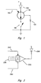
- Fig. 1 A prior art method of doing this, as used in the MCVVQ101 Backlight Driver integrated circuit from Motorola Inc. is shown in Fig. 1 .
- this driver the current flowing through LED 100 is controlled by current source 110 .
- the operating current is set by resistor 120 .
- Switch 130 represents a master on/off control, and control line 140 allows for brightness control.
- This design is replicated three times on a single integrated circuit to control red, green, and blue LEDs.
- individual resistors 120 for each of the red, green, and blue drivers must be carefully and individually selected. Achieving precise color balance in the presence of process variation in LED characteristics with this driver design requires careful trimming of resistors 120 .
- An alternative approach to obtaining precise color balance is to carefully prescreen LEDs and select only those within a narrow operating range.
- a third alternative is to sacrifice color balance by going with nominal or ballpark values for the performance of LEDs 100 and resistors 120 .
- None of these three alternatives is particularly palatable, incurring either extra cost in screening LEDs, incurring extra manufacturing cost and time in selecting or trimming resistors 120 , or sacrificing precise color balance.
- Fig. 2 shows a first embodiment of the present invention.
- a single color is shown; this design is replicated on the integrated circuit for each of the colors used, typically three times, for red, green, and blue.
- LED 200 is driven by multiplying digital to analog converter (MDAC) 220 . Multiplying digital to analog converters are known to the art, described for example in chapter 9 of The Art of Electronics, Second Edition, by Horowitz and Hill, Cambridge University Press, 1989.
- Digital inputs 230 control LED current.
- Control line 240 allows for intensity control, and is common to each MDAC so that a single control line 240 controls the operation of all MDACs..
- Control line 250 latches the data in MDAC 220 ; depending on the design, this latch may not be part of the MDAC, but may be part of the overall control circuitry (not shown). With this design, current through LED 200 is set digitally, allowing the operating point of each LED to be set easily during the manufacturing process, without needing to trim or select components such as resistors or LEDs, allowing close color balance to be achieved. In practice, four to six bits of resolution are adequate for MDAC 220 ; additional bits provide more resolution at the expense of increased pad complexity and size. While a current output MDAC is preferred in the present invention, it is understood that a voltage output MDACs may be used, each followed by a voltage to current converter.
- Fig. 3 shows a second embodiment of the present invention using a single MDAC multiplexed to drive three LEDs.
- LEDs 300, 302, and 304 connect to MDAC 320 through switches 319, 312, and 314 respectively.
- Digital lines 330 control the current, with line 340 providing intensity control and line 350 latching the data. As before, this latch may be part of MDAC 320 or may be part of the control circuitry.
- Fig. 3 multiplexes a single MDAC. This requires external control circuitry (not shown) to scan across the LEDs, closing switches 310, 312, and 314 while providing the correct digital inputs for the corresponding LED at digital inputs 330 and latch control 350 .
- Fig. 4 shows an embodiment of the present MDAC invention as implemented using complimentary metal oxide semiconductor (CMOS) technology. This structure is replicated for each of the different color LEDs driven. While a 4 bit device is shown, this may be extended as is known to the art. Data latching previously described is not shown.
- the MDAC may also be implemented using bipolar technology, or other MOS structures known to the art.
- LED 400 connects between positive supply terminal 402 and switching terminal 410 .
- Switches 420, 422, 424, 426 are controlled by their corresponding gates 430, 432, 434, 436.
- Current sources 440, 442, 444, 446 form a binary ladder, with each current source supplying twice the current of the previous.
- current source 440 causes 1x the design current to flow through LED 400 and switch 420
- current source 442 causes 2x the design current to flow
- current source 444 causes 4x the design current to flow, and so on.
- This binary weighting allows the current flowing through LED 400 to be easily adjusted by turning on the appropriate switches 420, 422, 424, 426.
- the gates of current sources 440, 442, 444, 446 are tied together and fed from a common source comprised of transistors 450, 452, 454, and 456 .
- the voltage on gates of current sources 440, 442, 444, 446 is varied, thereby changing the current flowing through the current sources.
- the level of the signal presented at node 460 is effectively multiplied by the binary weighting of the current sources ( 440, 442, 444, 446 ) which are activated by their corresponding gates 430, 432, 434, 436.
- Gate 470 of transistor 454 provides the ability to effectively shut down the converter.
- Transistor 456 provides isolation As in FIG 2 , node 480 for each of the MDACs present are tied together, providing common control of all MDACs. Transistor 456 provides isolation between sections of each MDAC.
- the MDAC of FIG 4 may also be combined with the multiplexing arrangement shown in FIG 3 for scanned LEDs.
Landscapes
- Engineering & Computer Science (AREA)
- Physics & Mathematics (AREA)
- Computer Hardware Design (AREA)
- General Physics & Mathematics (AREA)
- Theoretical Computer Science (AREA)
- Led Devices (AREA)
- Control Of Indicators Other Than Cathode Ray Tubes (AREA)
- Control Of El Displays (AREA)
Abstract
Description
Claims (12)
- Apparatus for driving a plurality of different color light emitting diodes comprising a plurality of multiplying digital to analog converters, one for each color of light emitting diode, the plurality of multiplying digital to analog converters integrated into a single integrated circuit.
- The apparatus of Claim 1 where three multiplying digital to analog converters are present on a single integrated circuit.
- The apparatus of Claim 1 where the resolution of each multiplying digital to analog converter is at least two bits.
- The apparatus of Claim 1 where the multiplying digital to analog converters are fabricated from CMOS.
- Apparatus for driving a plurality of different color light emitting diodes comprising a plurality of current output multiplying digital to analog converters integrated into a single integrated circuit, each multiplying digital to analog converter having a plurality of digital inputs, an analog input, and a current output for driving a particular color of light emitting diode, one multiplying digital to analog converter for each color of light emitting diode, the analog inputs of each of the multiplying digital to analog converters connected together to provide a common analog input.
- The apparatus of Claim 5 where three current output multiplying digital to analog converters are present.
- The apparatus of Claim 6 where the resolution of each multiplying digital to analog converter is at least two bits.
- The apparatus of Claim 7 where the least significant bit of each multiplying digital to analog converter is continuously enabled.
- The apparatus of Claim 6 where the multiplying digital to analog converters are fabricated from CMOS.
- Apparatus for driving a plurality of different color light emitting diodes comprising a single multiplying digital to analog converter having an analog input, a plurality of digital inputs, and an analog output, a multiplexer connected to the analog output of the digital to analog converter, the multiplexer having a plurality of outputs, one output for each color of light emitting diode, the multiplying digital to analog converter and the multiplexer present in a single integrated circuit.
- The apparatus of Claim 10 where the multiplexer has three outputs.
- The apparatus of Claim 10 where the resolution of the multiplying digital to analog converter is at least two bits.
Applications Claiming Priority (2)
| Application Number | Priority Date | Filing Date | Title |
|---|---|---|---|
| US303797 | 1999-04-30 | ||
| US09/303,797 US6266000B1 (en) | 1999-04-30 | 1999-04-30 | Programmable LED driver pad |
Publications (3)
| Publication Number | Publication Date |
|---|---|
| EP1049360A2 true EP1049360A2 (en) | 2000-11-02 |
| EP1049360A3 EP1049360A3 (en) | 2003-12-03 |
| EP1049360B1 EP1049360B1 (en) | 2007-05-09 |
Family
ID=23173744
Family Applications (1)
| Application Number | Title | Priority Date | Filing Date |
|---|---|---|---|
| EP00106754A Expired - Lifetime EP1049360B1 (en) | 1999-04-30 | 2000-03-29 | Programmable led driver pad |
Country Status (5)
| Country | Link |
|---|---|
| US (1) | US6266000B1 (en) |
| EP (1) | EP1049360B1 (en) |
| JP (1) | JP2000340842A (en) |
| KR (1) | KR100694371B1 (en) |
| DE (1) | DE60034737D1 (en) |
Cited By (10)
| Publication number | Priority date | Publication date | Assignee | Title |
|---|---|---|---|---|
| WO2002047438A3 (en) * | 2000-12-07 | 2002-10-31 | Koninkl Philips Electronics Nv | Led luminary system |
| EP1330143A3 (en) * | 2002-01-17 | 2004-02-11 | Patent-Treuhand-Gesellschaft für elektrische Glühlampen mbH | Operating device for light emitting diodes |
| JPWO2003027998A1 (en) * | 2001-09-25 | 2005-01-13 | 松下電器産業株式会社 | EL display device |
| SG119186A1 (en) * | 2002-05-17 | 2006-02-28 | Semiconductor Energy Lab | Display apparatus and driving method thereof |
| US7138967B2 (en) | 2001-09-21 | 2006-11-21 | Semiconductor Energy Laboratory Co., Ltd. | Display device and driving method thereof |
| US7170479B2 (en) | 2002-05-17 | 2007-01-30 | Semiconductor Energy Laboratory Co., Ltd. | Display device and driving method thereof |
| US7184034B2 (en) | 2002-05-17 | 2007-02-27 | Semiconductor Energy Laboratory Co., Ltd. | Display device |
| WO2007048747A1 (en) * | 2005-10-26 | 2007-05-03 | Patent-Treuhand-Gesellschaft für elektrische Glühlampen mbH | Circuit arrangement and method for adjusting the brightness of a light source arrangement |
| US7474285B2 (en) | 2002-05-17 | 2009-01-06 | Semiconductor Energy Laboratory Co., Ltd. | Display apparatus and driving method thereof |
| US7511687B2 (en) | 2002-05-17 | 2009-03-31 | Semiconductor Energy Laboratory Co., Ltd. | Display device, electronic apparatus and navigation system |
Families Citing this family (28)
| Publication number | Priority date | Publication date | Assignee | Title |
|---|---|---|---|---|
| JP2003022052A (en) * | 2001-07-10 | 2003-01-24 | Sony Corp | Driving circuit of light emitting element and image display device |
| US7012597B2 (en) * | 2001-08-02 | 2006-03-14 | Seiko Epson Corporation | Supply of a programming current to a pixel |
| JP2003233347A (en) * | 2001-08-02 | 2003-08-22 | Seiko Epson Corp | Supply programming current to pixels |
| JP4193452B2 (en) * | 2001-08-29 | 2008-12-10 | 日本電気株式会社 | Semiconductor device for driving current load device and current load device having the same |
| CN100440286C (en) | 2001-08-29 | 2008-12-03 | 日本电气株式会社 | Semiconductor device for driving current load device and current load device provided therewith |
| JP3903770B2 (en) * | 2001-11-08 | 2007-04-11 | 日本電気株式会社 | Data line drive circuit |
| GB0209502D0 (en) * | 2002-04-25 | 2002-06-05 | Cambridge Display Tech Ltd | Display driver circuits |
| JP2005524107A (en) * | 2002-04-25 | 2005-08-11 | ケンブリッジ ディスプレイ テクノロジー リミテッド | Display driver circuit for organic light-emitting diodes skipping blank lines |
| WO2003091977A1 (en) * | 2002-04-26 | 2003-11-06 | Toshiba Matsushita Display Technology Co., Ltd. | Driver circuit of el display panel |
| JP2007226258A (en) * | 2002-04-26 | 2007-09-06 | Toshiba Matsushita Display Technology Co Ltd | Driver circuit of el display panel |
| JP4630884B2 (en) * | 2002-04-26 | 2011-02-09 | 東芝モバイルディスプレイ株式会社 | EL display device driving method and EL display device |
| JP4653775B2 (en) * | 2002-04-26 | 2011-03-16 | 東芝モバイルディスプレイ株式会社 | Inspection method for EL display device |
| JP4266149B2 (en) * | 2002-10-07 | 2009-05-20 | ローム株式会社 | Organic EL drive circuit and organic EL display device using the same |
| JP3881645B2 (en) * | 2002-10-08 | 2007-02-14 | ローム株式会社 | Organic EL drive circuit and organic EL display device using the same |
| JP4247660B2 (en) * | 2002-11-28 | 2009-04-02 | カシオ計算機株式会社 | CURRENT GENERATION SUPPLY CIRCUIT, ITS CONTROL METHOD, AND DISPLAY DEVICE PROVIDED WITH CURRENT GENERATION SUPPLY CIRCUIT |
| JP4241144B2 (en) * | 2002-10-31 | 2009-03-18 | カシオ計算機株式会社 | DRIVE CONTROL DEVICE, ITS CONTROL METHOD, AND DISPLAY DEVICE PROVIDED WITH DRIVE CONTROL DEVICE |
| KR100803412B1 (en) * | 2002-10-31 | 2008-02-13 | 가시오게산키 가부시키가이샤 | Display device and method for driving display device |
| EP1623603A1 (en) * | 2003-05-07 | 2006-02-08 | Koninklijke Philips Electronics N.V. | Single driver for multiple light emitting diodes |
| KR100742063B1 (en) * | 2003-05-26 | 2007-07-23 | 가시오게산키 가부시키가이샤 | Electric current generation supply circuit and display device |
| JP2005017977A (en) * | 2003-06-30 | 2005-01-20 | Casio Comput Co Ltd | CURRENT GENERATION SUPPLY CIRCUIT AND DISPLAY DEVICE PROVIDED WITH THE CURRENT GENERATION SUPPLY CIRCUIT |
| JP4304585B2 (en) * | 2003-06-30 | 2009-07-29 | カシオ計算機株式会社 | CURRENT GENERATION SUPPLY CIRCUIT, CONTROL METHOD THEREOF, AND DISPLAY DEVICE PROVIDED WITH THE CURRENT GENERATION SUPPLY CIRCUIT |
| JP4103079B2 (en) * | 2003-07-16 | 2008-06-18 | カシオ計算機株式会社 | CURRENT GENERATION SUPPLY CIRCUIT, ITS CONTROL METHOD, AND DISPLAY DEVICE PROVIDED WITH CURRENT GENERATION SUPPLY CIRCUIT |
| US20050225264A1 (en) * | 2004-03-30 | 2005-10-13 | Kemp William H | LED lamp with color and brightness controller for use in wet, electrically hazardous bathing environments |
| US20060031599A1 (en) * | 2004-08-09 | 2006-02-09 | International Business Machines Corporation | Shared led control within a storage enclosure via modulation of a single led control signal |
| US20060214876A1 (en) * | 2005-03-23 | 2006-09-28 | Sony Ericsson Mobile Communications Ab | Electronic device having a light bus for controlling light emitting elements |
| JP4811434B2 (en) * | 2008-07-24 | 2011-11-09 | カシオ計算機株式会社 | CURRENT GENERATION SUPPLY CIRCUIT AND DISPLAY DEVICE PROVIDED WITH CURRENT GENERATION SUPPLY CIRCUIT |
| CN102752902B (en) * | 2011-04-22 | 2014-10-15 | 登丰微电子股份有限公司 | LED driver circuit |
| CN106211429B (en) * | 2016-07-14 | 2017-11-14 | 江苏万邦微电子有限公司 | A kind of large driven current density circuit |
Family Cites Families (7)
| Publication number | Priority date | Publication date | Assignee | Title |
|---|---|---|---|---|
| US4183046A (en) * | 1978-08-17 | 1980-01-08 | Interpretation Systems Incorporated | Electronic apparatus for converting digital image or graphics data to color video display formats and method therefor |
| US4464726A (en) * | 1981-09-08 | 1984-08-07 | Massachusetts Institute Of Technology | Charge domain parallel processing network |
| US4779029A (en) * | 1985-03-11 | 1988-10-18 | Ncr Corporation | Digitally compensated multiplying digital to analog converter |
| US4920344A (en) * | 1985-03-11 | 1990-04-24 | Ncr Corporation | Digitally compensated multiplying digital to analog converter |
| US4631522A (en) * | 1985-04-12 | 1986-12-23 | Audio Precision, Inc. | Method and circuit for compensation of a multiplying digital-to-analog converter |
| US5479189A (en) * | 1991-02-28 | 1995-12-26 | Chesavage; Jay | 4 channel color display adapter and method for color correction |
| JP3599883B2 (en) * | 1996-03-25 | 2004-12-08 | シャープ株式会社 | Light emitting element control device, optical sensor control device, and blank lamp control device |
-
1999
- 1999-04-30 US US09/303,797 patent/US6266000B1/en not_active Expired - Lifetime
-
2000
- 2000-03-29 EP EP00106754A patent/EP1049360B1/en not_active Expired - Lifetime
- 2000-03-29 DE DE60034737T patent/DE60034737D1/en not_active Expired - Lifetime
- 2000-04-27 KR KR1020000022401A patent/KR100694371B1/en not_active Expired - Lifetime
- 2000-04-27 JP JP2000127875A patent/JP2000340842A/en not_active Withdrawn
Cited By (16)
| Publication number | Priority date | Publication date | Assignee | Title |
|---|---|---|---|---|
| WO2002047438A3 (en) * | 2000-12-07 | 2002-10-31 | Koninkl Philips Electronics Nv | Led luminary system |
| CN1319417C (en) * | 2000-12-07 | 2007-05-30 | 皇家菲利浦电子有限公司 | LED luminary system |
| US7138967B2 (en) | 2001-09-21 | 2006-11-21 | Semiconductor Energy Laboratory Co., Ltd. | Display device and driving method thereof |
| US8599109B2 (en) | 2001-09-21 | 2013-12-03 | Semiconductor Energy Laboratory Co., Ltd. | Display device and driving method thereof |
| US7859520B2 (en) | 2001-09-21 | 2010-12-28 | Semiconductor Energy Laboratory Co., Ltd. | Display device and driving method thereof |
| JPWO2003027998A1 (en) * | 2001-09-25 | 2005-01-13 | 松下電器産業株式会社 | EL display device |
| EP1330143A3 (en) * | 2002-01-17 | 2004-02-11 | Patent-Treuhand-Gesellschaft für elektrische Glühlampen mbH | Operating device for light emitting diodes |
| US7474285B2 (en) | 2002-05-17 | 2009-01-06 | Semiconductor Energy Laboratory Co., Ltd. | Display apparatus and driving method thereof |
| SG119186A1 (en) * | 2002-05-17 | 2006-02-28 | Semiconductor Energy Lab | Display apparatus and driving method thereof |
| US7511687B2 (en) | 2002-05-17 | 2009-03-31 | Semiconductor Energy Laboratory Co., Ltd. | Display device, electronic apparatus and navigation system |
| US7532209B2 (en) | 2002-05-17 | 2009-05-12 | Semiconductor Energy Laboratory Co., Ltd. | Display apparatus and driving method thereof |
| US7852297B2 (en) | 2002-05-17 | 2010-12-14 | Semiconductor Energy Laboratory Co., Ltd. | Display device |
| US7184034B2 (en) | 2002-05-17 | 2007-02-27 | Semiconductor Energy Laboratory Co., Ltd. | Display device |
| US7864143B2 (en) | 2002-05-17 | 2011-01-04 | Semiconductor Energy Laboratory Co., Ltd. | Display device and driving method thereof |
| US7170479B2 (en) | 2002-05-17 | 2007-01-30 | Semiconductor Energy Laboratory Co., Ltd. | Display device and driving method thereof |
| WO2007048747A1 (en) * | 2005-10-26 | 2007-05-03 | Patent-Treuhand-Gesellschaft für elektrische Glühlampen mbH | Circuit arrangement and method for adjusting the brightness of a light source arrangement |
Also Published As
| Publication number | Publication date |
|---|---|
| EP1049360B1 (en) | 2007-05-09 |
| KR20010007020A (en) | 2001-01-26 |
| US6266000B1 (en) | 2001-07-24 |
| DE60034737D1 (en) | 2007-06-21 |
| KR100694371B1 (en) | 2007-03-12 |
| EP1049360A3 (en) | 2003-12-03 |
| JP2000340842A (en) | 2000-12-08 |
Similar Documents
| Publication | Publication Date | Title |
|---|---|---|
| US6266000B1 (en) | Programmable LED driver pad | |
| US10694597B2 (en) | LED pixel circuits with PWM dimming | |
| US9210753B2 (en) | Serial lighting interface with embedded feedback | |
| US7696962B2 (en) | Color balancing circuit for a display panel | |
| US10390405B2 (en) | Systems and methods of LED color overlap | |
| US8098028B2 (en) | Control circuit and method for controlling LEDs | |
| US7605547B2 (en) | Addressable LED architecture | |
| CN111833801B (en) | Display system and common driving circuit thereof | |
| US7551153B2 (en) | Combined exponential/linear RGB LED I-sink digital-to-analog converter | |
| US20090174343A1 (en) | Multiple LED Driver | |
| US7327091B2 (en) | Light-emitting element driving apparatus | |
| US8203506B2 (en) | LED drive circuit | |
| US11210997B2 (en) | Passive matrix LED display module and display with several passive matrix LED display modules | |
| TWI404000B (en) | Flat panel display driver | |
| US20070152909A1 (en) | Led device | |
| JP2001290465A (en) | Light emitting diode drive circuit | |
| JPH104213A (en) | Brightness adjustment device for light emitting element | |
| US12380820B2 (en) | Projection device, control circuit and control method thereof | |
| JP2003101073A (en) | Dual voltage power supply | |
| JPS63104095A (en) | Light emitting diode display device | |
| KR930006746Y1 (en) | Input level selection circuit | |
| JP2006203044A (en) | Led device | |
| JPH0628334B2 (en) | Switching circuit used for channel switching of TV etc. | |
| JPS58161416A (en) | Channel selection circuit | |
| JPH0117157B2 (en) |
Legal Events
| Date | Code | Title | Description |
|---|---|---|---|
| PUAI | Public reference made under article 153(3) epc to a published international application that has entered the european phase |
Free format text: ORIGINAL CODE: 0009012 |
|
| AK | Designated contracting states |
Kind code of ref document: A2 Designated state(s): AT BE CH CY DE DK ES FI FR GB GR IE IT LI LU MC NL PT SE |
|
| AX | Request for extension of the european patent |
Free format text: AL;LT;LV;MK;RO;SI |
|
| RAP1 | Party data changed (applicant data changed or rights of an application transferred) |
Owner name: AGILENT TECHNOLOGIES INC. |
|
| RAP1 | Party data changed (applicant data changed or rights of an application transferred) |
Owner name: AGILENT TECHNOLOGIES INC. A DELAWARE CORPORATION |
|
| RAP1 | Party data changed (applicant data changed or rights of an application transferred) |
Owner name: AGILENT TECHNOLOGIES, INC. (A DELAWARE CORPORATION |
|
| PUAL | Search report despatched |
Free format text: ORIGINAL CODE: 0009013 |
|
| AK | Designated contracting states |
Kind code of ref document: A3 Designated state(s): AT BE CH CY DE DK ES FI FR GB GR IE IT LI LU MC NL PT SE |
|
| AX | Request for extension of the european patent |
Extension state: AL LT LV MK RO SI |
|
| 17P | Request for examination filed |
Effective date: 20040204 |
|
| AKX | Designation fees paid |
Designated state(s): DE FR GB |
|
| 17Q | First examination report despatched |
Effective date: 20050218 |
|
| GRAP | Despatch of communication of intention to grant a patent |
Free format text: ORIGINAL CODE: EPIDOSNIGR1 |
|
| RAP1 | Party data changed (applicant data changed or rights of an application transferred) |
Owner name: AVAGO TECHNOLOGIES ECBU IP (SINGAPORE) PTE. LTD. |
|
| GRAS | Grant fee paid |
Free format text: ORIGINAL CODE: EPIDOSNIGR3 |
|
| GRAA | (expected) grant |
Free format text: ORIGINAL CODE: 0009210 |
|
| AK | Designated contracting states |
Kind code of ref document: B1 Designated state(s): DE FR GB |
|
| REG | Reference to a national code |
Ref country code: GB Ref legal event code: FG4D |
|
| REF | Corresponds to: |
Ref document number: 60034737 Country of ref document: DE Date of ref document: 20070621 Kind code of ref document: P |
|
| EN | Fr: translation not filed | ||
| PLBE | No opposition filed within time limit |
Free format text: ORIGINAL CODE: 0009261 |
|
| STAA | Information on the status of an ep patent application or granted ep patent |
Free format text: STATUS: NO OPPOSITION FILED WITHIN TIME LIMIT |
|
| 26N | No opposition filed |
Effective date: 20080212 |
|
| PG25 | Lapsed in a contracting state [announced via postgrant information from national office to epo] |
Ref country code: DE Free format text: LAPSE BECAUSE OF FAILURE TO SUBMIT A TRANSLATION OF THE DESCRIPTION OR TO PAY THE FEE WITHIN THE PRESCRIBED TIME-LIMIT Effective date: 20070810 |
|
| PG25 | Lapsed in a contracting state [announced via postgrant information from national office to epo] |
Ref country code: FR Free format text: LAPSE BECAUSE OF FAILURE TO SUBMIT A TRANSLATION OF THE DESCRIPTION OR TO PAY THE FEE WITHIN THE PRESCRIBED TIME-LIMIT Effective date: 20080104 |
|
| REG | Reference to a national code |
Ref country code: GB Ref legal event code: 732E Free format text: REGISTERED BETWEEN 20110728 AND 20110803 |
|
| REG | Reference to a national code |
Ref country code: GB Ref legal event code: 732E Free format text: REGISTERED BETWEEN 20160211 AND 20160217 |
|
| PGFP | Annual fee paid to national office [announced via postgrant information from national office to epo] |
Ref country code: GB Payment date: 20190327 Year of fee payment: 20 |
|
| REG | Reference to a national code |
Ref country code: GB Ref legal event code: PE20 Expiry date: 20200328 |
|
| PG25 | Lapsed in a contracting state [announced via postgrant information from national office to epo] |
Ref country code: GB Free format text: LAPSE BECAUSE OF EXPIRATION OF PROTECTION Effective date: 20200328 |