EP1049165A1 - Integrated circuit structure comprising a power circuit portion and a control circuit portion, without parasitic currents - Google Patents
Integrated circuit structure comprising a power circuit portion and a control circuit portion, without parasitic currents Download PDFInfo
- Publication number
- EP1049165A1 EP1049165A1 EP99830261A EP99830261A EP1049165A1 EP 1049165 A1 EP1049165 A1 EP 1049165A1 EP 99830261 A EP99830261 A EP 99830261A EP 99830261 A EP99830261 A EP 99830261A EP 1049165 A1 EP1049165 A1 EP 1049165A1
- Authority
- EP
- European Patent Office
- Prior art keywords
- well
- intermediate region
- integrated circuit
- type
- circuit
- Prior art date
- Legal status (The legal status is an assumption and is not a legal conclusion. Google has not performed a legal analysis and makes no representation as to the accuracy of the status listed.)
- Granted
Links
- 230000003071 parasitic effect Effects 0.000 title claims abstract description 42
- 239000000758 substrate Substances 0.000 claims abstract description 28
- 239000004065 semiconductor Substances 0.000 claims abstract description 27
- 239000000243 solution Substances 0.000 description 6
- 230000008901 benefit Effects 0.000 description 2
- 230000000694 effects Effects 0.000 description 2
- 238000002347 injection Methods 0.000 description 2
- 239000007924 injection Substances 0.000 description 2
- 229920006395 saturated elastomer Polymers 0.000 description 2
- 238000010276 construction Methods 0.000 description 1
- 238000010586 diagram Methods 0.000 description 1
- 238000002955 isolation Methods 0.000 description 1
- 230000007257 malfunction Effects 0.000 description 1
Images


Classifications
-
- H—ELECTRICITY
- H01—ELECTRIC ELEMENTS
- H01L—SEMICONDUCTOR DEVICES NOT COVERED BY CLASS H10
- H01L27/00—Devices consisting of a plurality of semiconductor or other solid-state components formed in or on a common substrate
- H01L27/02—Devices consisting of a plurality of semiconductor or other solid-state components formed in or on a common substrate including semiconductor components specially adapted for rectifying, oscillating, amplifying or switching and having potential barriers; including integrated passive circuit elements having potential barriers
- H01L27/04—Devices consisting of a plurality of semiconductor or other solid-state components formed in or on a common substrate including semiconductor components specially adapted for rectifying, oscillating, amplifying or switching and having potential barriers; including integrated passive circuit elements having potential barriers the substrate being a semiconductor body
- H01L27/08—Devices consisting of a plurality of semiconductor or other solid-state components formed in or on a common substrate including semiconductor components specially adapted for rectifying, oscillating, amplifying or switching and having potential barriers; including integrated passive circuit elements having potential barriers the substrate being a semiconductor body including only semiconductor components of a single kind
- H01L27/082—Devices consisting of a plurality of semiconductor or other solid-state components formed in or on a common substrate including semiconductor components specially adapted for rectifying, oscillating, amplifying or switching and having potential barriers; including integrated passive circuit elements having potential barriers the substrate being a semiconductor body including only semiconductor components of a single kind including bipolar components only
-
- H—ELECTRICITY
- H01—ELECTRIC ELEMENTS
- H01L—SEMICONDUCTOR DEVICES NOT COVERED BY CLASS H10
- H01L21/00—Processes or apparatus adapted for the manufacture or treatment of semiconductor or solid state devices or of parts thereof
- H01L21/70—Manufacture or treatment of devices consisting of a plurality of solid state components formed in or on a common substrate or of parts thereof; Manufacture of integrated circuit devices or of parts thereof
- H01L21/71—Manufacture of specific parts of devices defined in group H01L21/70
- H01L21/76—Making of isolation regions between components
- H01L21/761—PN junctions
-
- H—ELECTRICITY
- H01—ELECTRIC ELEMENTS
- H01L—SEMICONDUCTOR DEVICES NOT COVERED BY CLASS H10
- H01L27/00—Devices consisting of a plurality of semiconductor or other solid-state components formed in or on a common substrate
- H01L27/02—Devices consisting of a plurality of semiconductor or other solid-state components formed in or on a common substrate including semiconductor components specially adapted for rectifying, oscillating, amplifying or switching and having potential barriers; including integrated passive circuit elements having potential barriers
- H01L27/0203—Particular design considerations for integrated circuits
- H01L27/0248—Particular design considerations for integrated circuits for electrical or thermal protection, e.g. electrostatic discharge [ESD] protection
- H01L27/0251—Particular design considerations for integrated circuits for electrical or thermal protection, e.g. electrostatic discharge [ESD] protection for MOS devices
- H01L27/0259—Particular design considerations for integrated circuits for electrical or thermal protection, e.g. electrostatic discharge [ESD] protection for MOS devices using bipolar transistors as protective elements
-
- H—ELECTRICITY
- H01—ELECTRIC ELEMENTS
- H01L—SEMICONDUCTOR DEVICES NOT COVERED BY CLASS H10
- H01L27/00—Devices consisting of a plurality of semiconductor or other solid-state components formed in or on a common substrate
- H01L27/02—Devices consisting of a plurality of semiconductor or other solid-state components formed in or on a common substrate including semiconductor components specially adapted for rectifying, oscillating, amplifying or switching and having potential barriers; including integrated passive circuit elements having potential barriers
- H01L27/04—Devices consisting of a plurality of semiconductor or other solid-state components formed in or on a common substrate including semiconductor components specially adapted for rectifying, oscillating, amplifying or switching and having potential barriers; including integrated passive circuit elements having potential barriers the substrate being a semiconductor body
- H01L27/06—Devices consisting of a plurality of semiconductor or other solid-state components formed in or on a common substrate including semiconductor components specially adapted for rectifying, oscillating, amplifying or switching and having potential barriers; including integrated passive circuit elements having potential barriers the substrate being a semiconductor body including a plurality of individual components in a non-repetitive configuration
- H01L27/0611—Devices consisting of a plurality of semiconductor or other solid-state components formed in or on a common substrate including semiconductor components specially adapted for rectifying, oscillating, amplifying or switching and having potential barriers; including integrated passive circuit elements having potential barriers the substrate being a semiconductor body including a plurality of individual components in a non-repetitive configuration integrated circuits having a two-dimensional layout of components without a common active region
- H01L27/0617—Devices consisting of a plurality of semiconductor or other solid-state components formed in or on a common substrate including semiconductor components specially adapted for rectifying, oscillating, amplifying or switching and having potential barriers; including integrated passive circuit elements having potential barriers the substrate being a semiconductor body including a plurality of individual components in a non-repetitive configuration integrated circuits having a two-dimensional layout of components without a common active region comprising components of the field-effect type
- H01L27/0623—Devices consisting of a plurality of semiconductor or other solid-state components formed in or on a common substrate including semiconductor components specially adapted for rectifying, oscillating, amplifying or switching and having potential barriers; including integrated passive circuit elements having potential barriers the substrate being a semiconductor body including a plurality of individual components in a non-repetitive configuration integrated circuits having a two-dimensional layout of components without a common active region comprising components of the field-effect type in combination with bipolar transistors
Definitions
- This invention relates to an integrated circuit structure which comprises a power circuit portion and a control circuit portion and is free from parasitic currents.
- the invention specifically concerns an integrated circuit structure formed on a semiconductor substrate with conductivity of a first type, which structure comprises a first circuit portion incorporated to a first well and including at least one power transistor, and a second control circuit portion incorporated to a second well, and an intermediate region located between said first and second circuit portions, the conductivity of said first well, second well, and intermediate region being of a second type.
- the invention concerns, particularly but not exclusively, an integrated circuit structure, and the description which follows will cover that field of application for simplicity.
- a parasitic PNP transistor is created between the base of the power device and said P region.
- Figure 1 herewith shows, by way of example, a conventional integrated circuit 1' comprising a semiconductor substrate 2' of the N- type which is formed with a first well 3' of the P type provided for forming a power device, and a second well 4' -- also of the P type -- comprising the control region.
- a third well 5' of the N type is formed inside the first well 3', whereby the emitter terminal for the bipolar power transistor Power can be formed, which transistor will have its collector terminal in the semiconductor substrate 2' and its base terminal in the first well 3'.
- a fourth well 6' -- also of the N type -- is likewise formed inside the second well 4' and may be connected to a supply voltage reference Vcc, for example.
- the integrated circuit 1' will include a first parasitic transistor P1, whose emitter terminal is coincident with the base terminal of the bipolar transistor Power, i.e. with the first well 3'.
- the base terminal of this parasitic transistor is coincident with the collector terminal of the bipolar power transistor Power, i.e. with the semiconductor substrate 2', and its collector terminal is coincident with the second well 4' facing the bipolar power transistor Power.
- the value of the potential applied to its base terminal must be at least equal to, or higher than, the value of the potential applied to its emitter terminal.
- the second well 4' is essentially biased to a reference value Vbias through a resistive path which is represented by a resistive element R1.
- Vbias + R1*I - V(2) VbeP2
- a first known technical solution to the problem posed by the presence of parasitic transistors provides for that area of the semiconductor substrate 2' which lies intermediate between the first well 3' and the second 4' to be doped more heavily. In this way, the gain of the first parasitic transistor P1 is reduced.
- a second solution provides for increased spacing of the P-wells. Not even this solution is effective to suppress the flow of current brought about by the turning on of parasitic transistors.
- a third solution provides for an intermediate region 7', also of the P type, to be included between the aforementioned P-wells, as shown schematically in Figure 2.
- the underlying technical problem of this invention is to provide an integrated circuit, comprising a power device and a control region, with such structural and functional features as to eliminate the parasitic flow of current, thereby overcoming the drawbacks that still beset prior art integrated circuits.
- the concept behind this invention is one of having the intermediate region between the wells which accommodate the power device and the control region biased as a function of the potential of the well wherein the power device is formed.
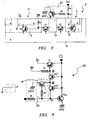
- an integrated electronic circuit is shown generally and schematically at 1 which includes a first power circuit portion comprising at least one power device 2, and a second control circuit portion 3.
- a region 4 is provided intermediate the first and second circuit portions.
- the integrated circuit 1 comprises a semiconductor substrate 5 of the N- type which has a first well 6 of the P type and a second well 7 of the P type formed therein for respectively accommodating the power device 2 and the control circuit portion or region 3.
- first 6 and second 7 wells Formed respectively inside the first 6 and second 7 wells are additional wells 8 and 9 of the N type.
- the well 9 inside the second well 7 will be connected, illustratively, to a supply voltage reference Vcc to create the control region 3.
- the second well 7 is essentially biased to a bias voltage reference Vbias through a resistive path represented by a resistive element R1.
- the bipolar power device PW is arranged to have its emitter terminal within the well 8, collector terminal in the semiconductor substrate 5, and base terminal within the first well 6.
- the integrated circuit 1 has a first parasitic transistor P2 whose emitter terminal is coincident with the semiconductor substrate 5, collector terminal is coincident with the well 9, and base terminal is coincident with the second well 7. Its base terminal will, therefore, be biased to the bias voltage reference Vbias via the resistive element R1.
- an intermediate region 4 also of the P type, is provided between the first well 6 and the second well 7 and substantially splits, between second P3' and third P3" parasitic transistors, the parasitic effect of the PNP junctions linked to said P-wells 6 and 7 associated with the semiconductor substrate 5 of the N type.
- the second parasitic transistor P3' has its emitter terminal coincident with the first well 6, collector terminal coincident with the intermediate region 4, and base terminal coincident with the semiconductor substrate 5.
- the third parasitic transistor P3" has its emitter terminal coincident with the intermediate region 4, collector terminal coincident with the second well 7, and base terminal coincident with the semiconductor substrate 5.
- a circuit means is arranged to bias the intermediate region 4 differently, according to the potential applied to the first well 6.
- This means comprises a biasing circuit 10 connected to said intermediate region 4 and said first well 6.
- the biasing circuit 10 comprises a bipolar transistor T having its emitter terminal connected to a voltage reference such as ground GND, collector terminal connected to the intermediate region 4, and base terminal connected to an output terminal OUT of the biasing circuit 10 through a series of first R2 and second R3 resistive elements.
- circuit node X intermediate the first R2 and second R3 resistive elements is connected to the first well 6.
- bipolar transistor T can be readily formed either inside the second well 7, i.e. in the control circuit portion of the integrated circuit, or in the intermediate region 4.
- the equivalent circuit 100 of Figure 4 comprises a power transistor PW which has its emitter terminal connected to the ground reference GND, base terminal connected to a first node 1 ⁇ , corresponding to the first well 6, and collector terminal connected to a second node 2 ⁇ , corresponding to the semiconductor substrate 5.
- the equivalent circuit 100 also includes a parasitic transistor P2 having its collector terminal connected to the supply voltage reference Vcc, emitter terminal connected to said second node 2 ⁇ , and base terminal connected to a third node 3 ⁇ corresponding to the second well 7.
- the third node 3 ⁇ is connected to a bias voltage reference Vbias through a resistive element R1.
- the equivalent circuit 100 includes a parasitic transistor P3' and a parasitic transistor P3", which are connected in series with each other between the first node 1 ⁇ and the third node 3 ⁇ and have their base terminals connected to the second node 2 ⁇ .
- the parasitic transistors P3' and P3'' are connected together at a fourth node 4 ⁇ , corresponding to the intermediate region 4 and itself connected to the collector terminal of the transistor T in the biasing circuit 10.
- the transistor T also has its emitter terminal connected to the ground reference GND, and its base terminal connected to the intermediate circuit node X via the resistive element R2.
- the intermediate circuit node X is connected to the first node 1 ⁇ , and connected to the output terminal OUT of the biasing circuit 10 via the resistive element R3.
- the combination of the transistor T and the resistive element R2 operates like a switch connected between the fourth node 4 ⁇ and ground GND and controlled by the potential at the first node 1 ⁇ , that is at the base terminal of the power device PW.
- the resistive element R2 functions as a decoupling element.
- the power device PW in the "on" state, its collector terminal may also go to a negative potential. In this case, a current would be caused to flow from the ground reference to the semiconductor substrate 5; therefore, the integrated circuit is normally provided with a diode which has its anode connected to the ground reference and its cathode connected to the semiconductor substrate 5.
- the transistor T of the biasing circuit 10 would be "on", and the intermediate region 4 biased all the same at the ground reference value.
- the transistor T of the biasing circuit 10 would be "on” all the same, and draw this current to the ground reference, thereby preventing the current from reaching the second well 7 through the parasitic transistor P3".
- the biasing circuit 10 keeps the potential applied to the intermediate region 4 at a lower value than, or the same value as, that of the semiconductor substrate 5, thereby ensuring that the parasitic transistor P3" is turned off.
- this parasitic transistor P3" has its base-emitter voltage Vbe near zero and, accordingly, will be "off” regardless of the value of potential at the second well 7.
- the value of the potential at the collector terminal would be normally clamped at 0.7V through a diode in parallel with the power device itself.
- the semiconductor substrate 5 When the semiconductor substrate 5 is at a value of potential equal to -0.7V, the first well 6, intermediate region 4, and second well 7 will all have a value of potential of approximately 0V, and the PN junctions (i.e., the diodes) formed by the above regions and the semiconductor substrate 5 will be forward biased.
- the PN junctions i.e., the diodes
- the transistor T of the biasing circuit 10 would be "off” in this case, since its base and collector terminals are at the same value of potential, which value is lower than, or equal to, the value of the potential at the emitter terminal (i.e., the ground reference value).
- the intermediate region 4 is “disjoined" from the biasing circuit 10, ensuring isolation of the voltage at the collector terminal of the power device from the regions 6 and 7.
- FIG. 5 Shown schematically in Figure 5 is a practical embodiment of the integrated circuit with biasing circuit 10 according to the invention, wherein the circuit 10 comprises a bipolar transistor T formed in the intermediate region 4.
- a first interior well 11 of the N type, providing the collector terminal for the bipolar transistor T, is formed in the intermediate region 4.
- a second interior well 12 of the P type providing the base terminal for the bipolar transistor T
- a third interior well 13 of the N type which provides the emitter terminal for the transistor T and is diffused inside the second interior well 12.
- the first interior well 11 is connected to the intermediate region 4 by an external short circuit.
- this external short circuit is produced in that area of the intermediate region which is facing the first well 6 accommodating the power device PW.
- the second interior well 12 is connected to the first well 6 through the resistive element R2, and connected to the output terminal OUT of the biasing circuit 10 through the additional resistive element R3.
Landscapes
- Engineering & Computer Science (AREA)
- Power Engineering (AREA)
- Physics & Mathematics (AREA)
- Condensed Matter Physics & Semiconductors (AREA)
- General Physics & Mathematics (AREA)
- Computer Hardware Design (AREA)
- Microelectronics & Electronic Packaging (AREA)
- Manufacturing & Machinery (AREA)
- Semiconductor Integrated Circuits (AREA)
- Metal-Oxide And Bipolar Metal-Oxide Semiconductor Integrated Circuits (AREA)
Abstract
Description
- This invention relates to an integrated circuit structure which comprises a power circuit portion and a control circuit portion and is free from parasitic currents.
- The invention specifically concerns an integrated circuit structure formed on a semiconductor substrate with conductivity of a first type, which structure comprises a first circuit portion incorporated to a first well and including at least one power transistor, and a second control circuit portion incorporated to a second well, and an intermediate region located between said first and second circuit portions, the conductivity of said first well, second well, and intermediate region being of a second type.
- The invention concerns, particularly but not exclusively, an integrated circuit structure, and the description which follows will cover that field of application for simplicity.
- As is well known, in an integrated electronic structure including a power circuit portion, specifically a bipolar type of power device with a vertical current flow, and a control circuit portion, such as a P-type region, a parasitic PNP transistor is created between the base of the power device and said P region.
- Figure 1 herewith shows, by way of example, a conventional integrated circuit 1' comprising a semiconductor substrate 2' of the N- type which is formed with a first well 3' of the P type provided for forming a power device, and a second well 4' -- also of the P type -- comprising the control region.
- In particular, where a bipolar power transistor Power is to be provided, a third well 5' of the N type is formed inside the first well 3', whereby the emitter terminal for the bipolar power transistor Power can be formed, which transistor will have its collector terminal in the semiconductor substrate 2' and its base terminal in the first well 3'.
- A fourth well 6' -- also of the N type -- is likewise formed inside the second well 4' and may be connected to a supply voltage reference Vcc, for example.
- Consequently, the integrated circuit 1' will include a first parasitic transistor P1, whose emitter terminal is coincident with the base terminal of the bipolar transistor Power, i.e. with the first well 3'. The base terminal of this parasitic transistor is coincident with the collector terminal of the bipolar power transistor Power, i.e. with the semiconductor substrate 2', and its collector terminal is coincident with the second well 4' facing the bipolar power transistor Power.
- In order for the first parasitic transistor P1 to be turned off, the value of the potential applied to its base terminal must be at least equal to, or higher than, the value of the potential applied to its emitter terminal.
- This condition is always met when the power device Power is operated in the linear range. But in most applications, the power device Power will be operated actually in the saturation range, since it is to serve a switching function.
- Under this operating condition, the base-collector junction of the bipolar power transistor Power, and hence the emitter-base junction of the first parasitic transistor P1, would be forward biased.
- There practically occurs a current injection from the first well 3', where the power transistor is formed, to the second well 4'. The value of this current is a function of the gain of the first parasitic transistor P1.
- The appearance of this current in the second well 4' causes malfunctioning of the control logic of the integrated circuit 1'. For the integrated circuit 1' to operate correctly, it is necessary that the potential at the second well 4' be lower than, or equal to, the potential at the semiconductor substrate 2' in which the bipolar power transistor Power and control circuit portion are both formed. It is only by meeting this restriction on potentials that the turning on of a second parasitic transistor P2, having its base terminal coincident with the second well 4', emitter terminal coincident with the semiconductor substrate 2', and collector terminal coincident with the fourth well 6', can be prevented.
- It should be considered, in particular, that the second well 4' is essentially biased to a reference value Vbias through a resistive path which is represented by a resistive element R1. When the injected current from the turning on of the first parasitic transistor P1 obeys the following relation:
- Vbias is the bias voltage of the second well 4';
- R1 is the resistance of the resistive path inside the second well 4';
- I is the current injected into the second well 4' from the turning on of the first parasitic transistor P1;
- V(2) is the value of the potential applied to the semiconductor substrate 2'; and
- VbeP2 is the base-emitter voltage of the second parasitic transistor P2; the parasitic transistor P2 is turned on, causing malfunctions to occur in the control region of the integrated circuit.
-
- A first known technical solution to the problem posed by the presence of parasitic transistors provides for that area of the semiconductor substrate 2' which lies intermediate between the first well 3' and the second 4' to be doped more heavily. In this way, the gain of the first parasitic transistor P1 is reduced.
- However, this dopage must not be carried too far, if the integrated circuit 1' is to be held at the correct voltage. In addition, the flow of current between the wells of the P type is reduced but not eliminated, with this solution.
- A second solution provides for increased spacing of the P-wells. Not even this solution is effective to suppress the flow of current brought about by the turning on of parasitic transistors.
- A third solution provides for an intermediate region 7', also of the P type, to be included between the aforementioned P-wells, as shown schematically in Figure 2.
- Unfortunately, this solution also has several drawbacks:
- 1) Where the intermediate region 7' is a floating region, a self-biasing of the intermediate region 7' to the value of potential of the first well 3' is precipitated upon a parasitic PNP transistor P1', associated with the well 3' and the intermediate region 7', entering its saturation range. As a result, an additional parasitic transistor P1", associated with the second well 4' and the region 7', is caused to move into its conduction range. The net effect of providing this intermediate region 7' is one of lowering the current gain of the parasitic elements as a whole: the net effect of the parasitic components is split between the two transistors, P1' and P1", but one (P1') of then will be in its saturation range.
- 2) When the intermediate region 7' is connected to a voltage reference, e.g. to ground, and by reason of the application involved the second well 4' is biased to a potential level below ground, the parasitic transistor P1" will move into its conduction range and draw current from the ground reference terminal to the second well 4'.
-
- The underlying technical problem of this invention is to provide an integrated circuit, comprising a power device and a control region, with such structural and functional features as to eliminate the parasitic flow of current, thereby overcoming the drawbacks that still beset prior art integrated circuits.
- The concept behind this invention is one of having the intermediate region between the wells which accommodate the power device and the control region biased as a function of the potential of the well wherein the power device is formed.
- Based on this concept, the technical problem is solved by an integrated circuit structure as previously indicated and defined in the characterizing portion of
Claim 1. - The features and advantages of an integrated circuit structure according to the invention will become apparent from the following description of an embodiment thereof, given by way of non-limitative example with reference to the accompanying drawings.
- In the drawings:
- Figure 1 shows schematically an integrated circuit which includes at least one power device and a control region, according to the prior art;
- Figure 2 shows schematically an alternative embodiment of the integrated circuit of Figure 1;
- Figure 3 shows schematically an integrated circuit according to this invention, which includes at least one power circuit portion and a control circuit portion;
- Figure 4 shows an equivalent electric diagram of the integrated circuit of Figure 3;
- Figure 5 shows schematically an embodiment of the integrated circuit of Figure 4.
-
- Referring to the drawing views, specifically to the example of Figure 3, an integrated electronic circuit is shown generally and schematically at 1 which includes a first power circuit portion comprising at least one
power device 2, and a secondcontrol circuit portion 3. Aregion 4 is provided intermediate the first and second circuit portions. - In particular, the integrated
circuit 1 comprises asemiconductor substrate 5 of the N- type which has a first well 6 of the P type and a second well 7 of the P type formed therein for respectively accommodating thepower device 2 and the control circuit portion orregion 3. - Formed respectively inside the first 6 and second 7 wells are
additional wells well 9 inside the second well 7 will be connected, illustratively, to a supply voltage reference Vcc to create thecontrol region 3. Further, the second well 7 is essentially biased to a bias voltage reference Vbias through a resistive path represented by a resistive element R1. - The bipolar power device PW is arranged to have its emitter terminal within the
well 8, collector terminal in thesemiconductor substrate 5, and base terminal within the first well 6. - The presence of NPN junctions at said wells 6 and 7 of the P type, combined with a
semiconductor substrate 5 of the N type, originates parasitic components. In particular, theintegrated circuit 1 has a first parasitic transistor P2 whose emitter terminal is coincident with thesemiconductor substrate 5, collector terminal is coincident with thewell 9, and base terminal is coincident with the second well 7. Its base terminal will, therefore, be biased to the bias voltage reference Vbias via the resistive element R1. - As previously mentioned in connection with the conventional integrated circuit, an
intermediate region 4, also of the P type, is provided between the first well 6 and the second well 7 and substantially splits, between second P3' and third P3" parasitic transistors, the parasitic effect of the PNP junctions linked to said P-wells 6 and 7 associated with thesemiconductor substrate 5 of the N type. - In particular, the second parasitic transistor P3' has its emitter terminal coincident with the first well 6, collector terminal coincident with the
intermediate region 4, and base terminal coincident with thesemiconductor substrate 5. Likewise, the third parasitic transistor P3" has its emitter terminal coincident with theintermediate region 4, collector terminal coincident with the second well 7, and base terminal coincident with thesemiconductor substrate 5. - Advantageously in this invention, a circuit means is arranged to bias the
intermediate region 4 differently, according to the potential applied to the first well 6. This means comprises a biasingcircuit 10 connected to saidintermediate region 4 and said first well 6. - More particularly, the biasing
circuit 10 comprises a bipolar transistor T having its emitter terminal connected to a voltage reference such as ground GND, collector terminal connected to theintermediate region 4, and base terminal connected to an output terminal OUT of the biasingcircuit 10 through a series of first R2 and second R3 resistive elements. - In addition, a circuit node X intermediate the first R2 and second R3 resistive elements is connected to the first well 6.
- It should be noted here that any controlled switch could be substituted for the transistor T.
- The use of a bipolar transistor actually makes for a simpler overall construction of the integrated circuit. In fact, a bipolar transistor T can be readily formed either inside the second well 7, i.e. in the control circuit portion of the integrated circuit, or in the
intermediate region 4. - In particular, efficiency would largely benefit from a transistor T being formed in the
intermediate region 4. - To make the operation of the integrated circuit containing a biasing
circuit 10 according to the invention more easily understood, its equivalent circuit shown in Figure 4 will be discussed first. - In particular, the
equivalent circuit 100 of Figure 4 comprises a power transistor PW which has its emitter terminal connected to the ground reference GND, base terminal connected to afirst node 1 ○, corresponding to the first well 6, and collector terminal connected to asecond node 2 ○, corresponding to thesemiconductor substrate 5. - The
equivalent circuit 100 also includes a parasitic transistor P2 having its collector terminal connected to the supply voltage reference Vcc, emitter terminal connected to saidsecond node 2 ○, and base terminal connected to athird node 3 ○ corresponding to the second well 7. - As previously explained, the
third node 3 ○ is connected to a bias voltage reference Vbias through a resistive element R1. - Finally, the
equivalent circuit 100 includes a parasitic transistor P3' and a parasitic transistor P3", which are connected in series with each other between thefirst node 1 ○and thethird node 3 ○ and have their base terminals connected to thesecond node 2 ○. - The parasitic transistors P3' and P3'' are connected together at a
fourth node 4 ○, corresponding to theintermediate region 4 and itself connected to the collector terminal of the transistor T in the biasingcircuit 10. - The transistor T also has its emitter terminal connected to the ground reference GND, and its base terminal connected to the intermediate circuit node X via the resistive element R2. The intermediate circuit node X is connected to the
first node 1 ○, and connected to the output terminal OUT of the biasingcircuit 10 via the resistive element R3. - As a matter of fact, the combination of the transistor T and the resistive element R2 operates like a switch connected between the
fourth node 4 ○and ground GND and controlled by the potential at thefirst node 1 ○, that is at the base terminal of the power device PW. Thus, the resistive element R2 functions as a decoupling element. - Against the background of the
equivalent circuit 100 just described, the circuit action under different conditions of operation can now be analysed: - 1. with the power device PW in the "on" state, the collector terminal can either have a value of potential close to the ground reference GND value ("saturated device") or a value of a few Volts ("unsaturated device"), while the base terminal is set at the value of the base-emitter voltage (Vbe) in the conduction range;
- 2. with the power device PW in the "off" state, the collector terminal goes to a high voltage value which will be specific to a particular application.
-
- It should be noted that, with the power device PW in the "on" state, its collector terminal may also go to a negative potential. In this case, a current would be caused to flow from the ground reference to the
semiconductor substrate 5; therefore, the integrated circuit is normally provided with a diode which has its anode connected to the ground reference and its cathode connected to thesemiconductor substrate 5. - In the instance of an unsaturated device being "on", its base-emitter junction is always reverse biased, and the parasitic transistors P3', P3" would be "off" regardless of the value of the potential at which the
intermediate region 4 is biased. - In this case, the transistor T of the biasing
circuit 10 would be "on", and theintermediate region 4 biased all the same at the ground reference value. - In the instance of a saturated device being "on", its base-emitter junction is forward biased, and the parasitic transistor P3' would be "on", whereby a current would be injected into the
intermediate region 4. - Advantageously in this invention, the transistor T of the biasing
circuit 10 would be "on" all the same, and draw this current to the ground reference, thereby preventing the current from reaching the second well 7 through the parasitic transistor P3". - Furthermore, the biasing
circuit 10 keeps the potential applied to theintermediate region 4 at a lower value than, or the same value as, that of thesemiconductor substrate 5, thereby ensuring that the parasitic transistor P3" is turned off. In fact, this parasitic transistor P3" has its base-emitter voltage Vbe near zero and, accordingly, will be "off" regardless of the value of potential at the second well 7. - In the event of the device being "on" in a "below ground" condition, that is for high values of the potential at its external base terminal or contact, the value of the potential at the collector terminal would be normally clamped at 0.7V through a diode in parallel with the power device itself.
- When the
semiconductor substrate 5 is at a value of potential equal to -0.7V, the first well 6,intermediate region 4, and second well 7 will all have a value of potential of approximately 0V, and the PN junctions (i.e., the diodes) formed by the above regions and thesemiconductor substrate 5 will be forward biased. - Advantageously in this invention, the transistor T of the biasing
circuit 10 would be "off" in this case, since its base and collector terminals are at the same value of potential, which value is lower than, or equal to, the value of the potential at the emitter terminal (i.e., the ground reference value). - Thus, the
intermediate region 4 is "disjoined" from the biasingcircuit 10, ensuring isolation of the voltage at the collector terminal of the power device from the regions 6 and 7. - In this way, the conduction of the parasitic transistor P3" and consequent injection of current into the second well 7 are prevented.
- Lastly, with a device in the "off" state, the value of potential of the
semiconductor substrate 5 will always be higher than the value of potential of the P regions, and no parasitic PNP transistors would be "on" between said regions and thesemiconductor substrate 5. - Shown schematically in Figure 5 is a practical embodiment of the integrated circuit with biasing
circuit 10 according to the invention, wherein thecircuit 10 comprises a bipolar transistor T formed in theintermediate region 4. - In particular, a first interior well 11 of the N type, providing the collector terminal for the bipolar transistor T, is formed in the
intermediate region 4. - Inside this first interior well 11, there are diffused a second interior well 12 of the P type, providing the base terminal for the bipolar transistor T, and a third interior well 13 of the N type which provides the emitter terminal for the transistor T and is diffused inside the second interior well 12.
- Advantageously in this invention, the first interior well 11 is connected to the
intermediate region 4 by an external short circuit. In particular, this external short circuit is produced in that area of the intermediate region which is facing the first well 6 accommodating the power device PW. - Further, the second interior well 12 is connected to the first well 6 through the resistive element R2, and connected to the output terminal OUT of the biasing
circuit 10 through the additional resistive element R3. - Finally, the third
interior well 13 is connected to the ground reference GND. - To summarize, with the integrated circuit of this invention, all current flows due to the presence of parasitic PNP transistors between the P-type wells and the N-type substrate can be cut off, through the
intermediate region 4 of the P type being connected between the power circuit portion and the control portion and biased by means of the biasingcircuit 10 to suit varying conditions of the power device operation.
Claims (9)
- An integrated circuit structure of the type formed on a semiconductor substrate (5) with conductivity of a first type (N), comprising a first circuit portion (2) incorporated into a first well (6) and including at least one power transistor, and a second control circuit portion (3) incorporated into a second well (7), and comprising an intermediate region (4) located between said first and second circuit portions, said first well (6), second well (7) and intermediate region (4) having conductivity of a second type (P), characterized in that it comprises a circuit means of biasing said intermediate region (4) at a value of potential tied to the value of potential of said first well (6), thereby cutting off a flow of parasitic current from said wells (6,7) to the semiconductor substrate (5).
- An integrated circuit structure according to Claim 1, characterized in that said circuit means for biasing the intermediate region (4) comprises a biasing circuit (10) connected to said intermediate region and said first well (6) and including at least one controlled switch.
- An integrated circuit structure according to Claim 2, characterized in that said controlled switch essentially includes a first terminal connected to a voltage reference (GND), a second terminal connected to said intermediate region (4), and a control terminal connected to an output terminal (OUT) of the biasing circuit (10).
- An integrated circuit structure according to Claim 3, characterized in that said biasing circuit (10) further comprises first (R2) and second (R3) resistive elements connected between the control terminal of said controlled switch and the output terminal (OUT) of the biasing circuit (10) .
- An integrated circuit structure according to Claim 3, characterized in that said controlled switch essentially comprises a bipolar transistor (T) having an emitter terminal connected to a voltage reference (GND), a collector terminal connected to said intermediate region (4), and a base terminal connected to an output terminal (OUT) of the biasing circuit (10).
- An integrated circuit structure according to Claim 5, characterized in that said bipolar transistor (T) is formed inside said second well (7).
- An integrated circuit structure according to Claim 5, characterized in that said bipolar transistor (T) is formed within said intermediate region (4).
- An integrated circuit structure according to Claim 7, characterized in that said intermediate region (4) is formed with a first interior well (11) having the first type (N) of conductivity, that a second interior well (12) having the second type (P) of conductivity is formed inside said first interior well (11), and that a third interior well (13) having the first type (N) of conductivity is formed inside said second interior well (12).
- An integrated circuit structure according to Claim 8, characterized in that said first interior well (11) is linked to the intermediate region (4) through an external short circuit produced in that area of the intermediate region (4) which is facing the first well (6).
Priority Applications (3)
| Application Number | Priority Date | Filing Date | Title |
|---|---|---|---|
| EP99830261A EP1049165B1 (en) | 1999-04-30 | 1999-04-30 | Integrated circuit structure comprising a power circuit portion and a control circuit portion, without parasitic currents |
| DE69902877T DE69902877D1 (en) | 1999-04-30 | 1999-04-30 | Integrated circuit with a power circuit and a control circuit, without parasitic currents |
| US09/560,195 US6337503B1 (en) | 1999-04-30 | 2000-04-28 | Integrated power circuit with reduced parasitic current flow |
Applications Claiming Priority (1)
| Application Number | Priority Date | Filing Date | Title |
|---|---|---|---|
| EP99830261A EP1049165B1 (en) | 1999-04-30 | 1999-04-30 | Integrated circuit structure comprising a power circuit portion and a control circuit portion, without parasitic currents |
Publications (2)
| Publication Number | Publication Date |
|---|---|
| EP1049165A1 true EP1049165A1 (en) | 2000-11-02 |
| EP1049165B1 EP1049165B1 (en) | 2002-09-11 |
Family
ID=8243387
Family Applications (1)
| Application Number | Title | Priority Date | Filing Date |
|---|---|---|---|
| EP99830261A Expired - Lifetime EP1049165B1 (en) | 1999-04-30 | 1999-04-30 | Integrated circuit structure comprising a power circuit portion and a control circuit portion, without parasitic currents |
Country Status (3)
| Country | Link |
|---|---|
| US (1) | US6337503B1 (en) |
| EP (1) | EP1049165B1 (en) |
| DE (1) | DE69902877D1 (en) |
Cited By (1)
| Publication number | Priority date | Publication date | Assignee | Title |
|---|---|---|---|---|
| EP4274074A1 (en) * | 2022-05-02 | 2023-11-08 | NXP USA, Inc. | Isolation connections for high-voltage power stage |
Families Citing this family (2)
| Publication number | Priority date | Publication date | Assignee | Title |
|---|---|---|---|---|
| JP4610199B2 (en) * | 2004-01-14 | 2011-01-12 | ルネサスエレクトロニクス株式会社 | Semiconductor integrated circuit for DC-DC converter and DC-DC converter |
| DE102017109264B3 (en) * | 2017-04-28 | 2018-08-23 | Infineon Technologies Ag | Power semiconductor devices and a method of forming a power semiconductor device |
Citations (4)
| Publication number | Priority date | Publication date | Assignee | Title |
|---|---|---|---|---|
| EP0512605A1 (en) * | 1991-05-03 | 1992-11-11 | Koninklijke Philips Electronics N.V. | Power device having reverse-voltage protection |
| EP0703620A1 (en) * | 1994-09-21 | 1996-03-27 | STMicroelectronics S.r.l. | Circuit for preventing turn-on of parasitic components in integrated circuits including a power stage and low-voltage control circuitry |
| US5550701A (en) * | 1994-08-30 | 1996-08-27 | International Rectifier Corporation | Power MOSFET with overcurrent and over-temperature protection and control circuit decoupled from body diode |
| EP0847089A1 (en) * | 1996-12-09 | 1998-06-10 | STMicroelectronics S.r.l. | Method and device for suppressing parasitic effects in a junction-insulated integrated circuit |
Family Cites Families (3)
| Publication number | Priority date | Publication date | Assignee | Title |
|---|---|---|---|---|
| FR2725307B1 (en) * | 1994-09-30 | 1996-12-20 | Sgs Thomson Microelectronics | SEMICONDUCTOR COMPONENT FOR FEEDING, RECIRCULATION AND DEMAGNETIZATION OF A SELFIC CHARGE |
| JPH0969572A (en) * | 1995-09-01 | 1997-03-11 | Toshiba Microelectron Corp | Semiconductor device and its manufacture |
| EP0782197B1 (en) * | 1995-12-29 | 2001-06-06 | Co.Ri.M.Me. Consorzio Per La Ricerca Sulla Microelettronica Nel Mezzogiorno | Integrated electronic device with reduced parasitic currents, and corresponding method |
-
1999
- 1999-04-30 DE DE69902877T patent/DE69902877D1/en not_active Expired - Lifetime
- 1999-04-30 EP EP99830261A patent/EP1049165B1/en not_active Expired - Lifetime
-
2000
- 2000-04-28 US US09/560,195 patent/US6337503B1/en not_active Expired - Lifetime
Patent Citations (4)
| Publication number | Priority date | Publication date | Assignee | Title |
|---|---|---|---|---|
| EP0512605A1 (en) * | 1991-05-03 | 1992-11-11 | Koninklijke Philips Electronics N.V. | Power device having reverse-voltage protection |
| US5550701A (en) * | 1994-08-30 | 1996-08-27 | International Rectifier Corporation | Power MOSFET with overcurrent and over-temperature protection and control circuit decoupled from body diode |
| EP0703620A1 (en) * | 1994-09-21 | 1996-03-27 | STMicroelectronics S.r.l. | Circuit for preventing turn-on of parasitic components in integrated circuits including a power stage and low-voltage control circuitry |
| EP0847089A1 (en) * | 1996-12-09 | 1998-06-10 | STMicroelectronics S.r.l. | Method and device for suppressing parasitic effects in a junction-insulated integrated circuit |
Cited By (1)
| Publication number | Priority date | Publication date | Assignee | Title |
|---|---|---|---|---|
| EP4274074A1 (en) * | 2022-05-02 | 2023-11-08 | NXP USA, Inc. | Isolation connections for high-voltage power stage |
Also Published As
| Publication number | Publication date |
|---|---|
| US6337503B1 (en) | 2002-01-08 |
| EP1049165B1 (en) | 2002-09-11 |
| DE69902877D1 (en) | 2002-10-17 |
Similar Documents
| Publication | Publication Date | Title |
|---|---|---|
| US5028811A (en) | Circuit for controlling a power MOS transistor on an inductive load | |
| US4577211A (en) | Integrated circuit and method for biasing an epitaxial layer | |
| US5703520A (en) | Integrated inductive load snubbing device using a multi-collector transistor | |
| US5051612A (en) | Prevention of parasitic mechanisms in junction isolated devices | |
| EP1049165B1 (en) | Integrated circuit structure comprising a power circuit portion and a control circuit portion, without parasitic currents | |
| US6870417B2 (en) | Circuit for loss-less diode equivalent | |
| CA1097752A (en) | Current mirror circuit | |
| JPH1079472A (en) | Semiconductor integrated circuit | |
| EP0313746A2 (en) | ECL input circuit for CMOS devices | |
| US5694075A (en) | Substrate clamp for non-isolated integrated circuits | |
| US5627715A (en) | Circuit construction for protective biasing | |
| US4301382A (en) | I2L With PNPN injector | |
| JP3610683B2 (en) | Analog switch circuit | |
| JP3179630B2 (en) | Epitaxial tub bias structure and integrated circuit | |
| WO1981000924A1 (en) | Current source having saturation protection | |
| US4185212A (en) | Level shifting circuit | |
| US6815779B1 (en) | Integrated circuit including protection against polarity inversion of the substrate potential | |
| US6034561A (en) | Integrated inductive load snubbing device | |
| JP3338738B2 (en) | PMOS output circuit | |
| US4689500A (en) | Comparator with substrate injection protection | |
| US6624502B2 (en) | Method and device for limiting the substrate potential in junction isolated integrated circuits | |
| JPH0249061B2 (en) | ||
| JP3135363B2 (en) | Semiconductor integrated circuit | |
| JP3570338B2 (en) | Power supply reverse connection protection circuit | |
| JP2878817B2 (en) | Electrostatic protection circuit |
Legal Events
| Date | Code | Title | Description |
|---|---|---|---|
| PUAI | Public reference made under article 153(3) epc to a published international application that has entered the european phase |
Free format text: ORIGINAL CODE: 0009012 |
|
| AK | Designated contracting states |
Kind code of ref document: A1 Designated state(s): DE FR GB IT |
|
| AX | Request for extension of the european patent |
Free format text: AL;LT;LV;MK;RO;SI |
|
| 17P | Request for examination filed |
Effective date: 20010130 |
|
| AKX | Designation fees paid |
Free format text: DE FR GB IT |
|
| GRAG | Despatch of communication of intention to grant |
Free format text: ORIGINAL CODE: EPIDOS AGRA |
|
| 17Q | First examination report despatched |
Effective date: 20010910 |
|
| GRAG | Despatch of communication of intention to grant |
Free format text: ORIGINAL CODE: EPIDOS AGRA |
|
| GRAH | Despatch of communication of intention to grant a patent |
Free format text: ORIGINAL CODE: EPIDOS IGRA |
|
| GRAH | Despatch of communication of intention to grant a patent |
Free format text: ORIGINAL CODE: EPIDOS IGRA |
|
| GRAA | (expected) grant |
Free format text: ORIGINAL CODE: 0009210 |
|
| AK | Designated contracting states |
Kind code of ref document: B1 Designated state(s): DE FR GB IT |
|
| PG25 | Lapsed in a contracting state [announced via postgrant information from national office to epo] |
Ref country code: FR Free format text: LAPSE BECAUSE OF NON-PAYMENT OF DUE FEES Effective date: 20020911 |
|
| REG | Reference to a national code |
Ref country code: GB Ref legal event code: FG4D |
|
| REF | Corresponds to: |
Ref document number: 69902877 Country of ref document: DE Date of ref document: 20021017 |
|
| PG25 | Lapsed in a contracting state [announced via postgrant information from national office to epo] |
Ref country code: DE Free format text: LAPSE BECAUSE OF FAILURE TO SUBMIT A TRANSLATION OF THE DESCRIPTION OR TO PAY THE FEE WITHIN THE PRESCRIBED TIME-LIMIT Effective date: 20021212 |
|
| EN | Fr: translation not filed | ||
| PLBE | No opposition filed within time limit |
Free format text: ORIGINAL CODE: 0009261 |
|
| STAA | Information on the status of an ep patent application or granted ep patent |
Free format text: STATUS: NO OPPOSITION FILED WITHIN TIME LIMIT |
|
| 26N | No opposition filed |
Effective date: 20030612 |
|
| PGFP | Annual fee paid to national office [announced via postgrant information from national office to epo] |
Ref country code: IT Payment date: 20070608 Year of fee payment: 9 |
|
| PG25 | Lapsed in a contracting state [announced via postgrant information from national office to epo] |
Ref country code: IT Free format text: LAPSE BECAUSE OF NON-PAYMENT OF DUE FEES Effective date: 20080430 |
|
| PGFP | Annual fee paid to national office [announced via postgrant information from national office to epo] |
Ref country code: GB Payment date: 20110330 Year of fee payment: 13 |
|
| GBPC | Gb: european patent ceased through non-payment of renewal fee |
Effective date: 20120430 |
|
| PG25 | Lapsed in a contracting state [announced via postgrant information from national office to epo] |
Ref country code: GB Free format text: LAPSE BECAUSE OF NON-PAYMENT OF DUE FEES Effective date: 20120430 |