EP1049162A2 - Interconnection structure of a multilayer circuit board for electrical connection to a semiconductor package and manufacturing method thereof - Google Patents
Interconnection structure of a multilayer circuit board for electrical connection to a semiconductor package and manufacturing method thereof Download PDFInfo
- Publication number
- EP1049162A2 EP1049162A2 EP00108979A EP00108979A EP1049162A2 EP 1049162 A2 EP1049162 A2 EP 1049162A2 EP 00108979 A EP00108979 A EP 00108979A EP 00108979 A EP00108979 A EP 00108979A EP 1049162 A2 EP1049162 A2 EP 1049162A2
- Authority
- EP
- European Patent Office
- Prior art keywords
- circuit board
- printed circuit
- pad
- set forth
- connection
- Prior art date
- Legal status (The legal status is an assumption and is not a legal conclusion. Google has not performed a legal analysis and makes no representation as to the accuracy of the status listed.)
- Withdrawn
Links
Images



Classifications
-
- H—ELECTRICITY
- H05—ELECTRIC TECHNIQUES NOT OTHERWISE PROVIDED FOR
- H05K—PRINTED CIRCUITS; CASINGS OR CONSTRUCTIONAL DETAILS OF ELECTRIC APPARATUS; MANUFACTURE OF ASSEMBLAGES OF ELECTRICAL COMPONENTS
- H05K1/00—Printed circuits
- H05K1/02—Details
- H05K1/11—Printed elements for providing electric connections to or between printed circuits
- H05K1/111—Pads for surface mounting, e.g. lay-out
- H05K1/112—Pads for surface mounting, e.g. lay-out directly combined with via connections
-
- H—ELECTRICITY
- H05—ELECTRIC TECHNIQUES NOT OTHERWISE PROVIDED FOR
- H05K—PRINTED CIRCUITS; CASINGS OR CONSTRUCTIONAL DETAILS OF ELECTRIC APPARATUS; MANUFACTURE OF ASSEMBLAGES OF ELECTRICAL COMPONENTS
- H05K3/00—Apparatus or processes for manufacturing printed circuits
- H05K3/30—Assembling printed circuits with electric components, e.g. with resistors
- H05K3/32—Assembling printed circuits with electric components, e.g. with resistors electrically connecting electric components or wires to printed circuits
- H05K3/34—Assembling printed circuits with electric components, e.g. with resistors electrically connecting electric components or wires to printed circuits by soldering
- H05K3/341—Surface mounted components
- H05K3/3431—Leadless components
- H05K3/3436—Leadless components having an array of bottom contacts, e.g. pad grid array or ball grid array components
-
- H—ELECTRICITY
- H10—SEMICONDUCTOR DEVICES; ELECTRIC SOLID-STATE DEVICES NOT OTHERWISE PROVIDED FOR
- H10W—GENERIC PACKAGES, INTERCONNECTIONS, CONNECTORS OR OTHER CONSTRUCTIONAL DETAILS OF DEVICES COVERED BY CLASS H10
- H10W70/00—Package substrates; Interposers; Redistribution layers [RDL]
- H10W70/60—Insulating or insulated package substrates; Interposers; Redistribution layers
- H10W70/611—Insulating or insulated package substrates; Interposers; Redistribution layers for connecting multiple chips together
-
- H—ELECTRICITY
- H10—SEMICONDUCTOR DEVICES; ELECTRIC SOLID-STATE DEVICES NOT OTHERWISE PROVIDED FOR
- H10W—GENERIC PACKAGES, INTERCONNECTIONS, CONNECTORS OR OTHER CONSTRUCTIONAL DETAILS OF DEVICES COVERED BY CLASS H10
- H10W72/00—Interconnections or connectors in packages
- H10W72/20—Bump connectors, e.g. solder bumps or copper pillars; Dummy bumps; Thermal bumps
-
- H—ELECTRICITY
- H10—SEMICONDUCTOR DEVICES; ELECTRIC SOLID-STATE DEVICES NOT OTHERWISE PROVIDED FOR
- H10W—GENERIC PACKAGES, INTERCONNECTIONS, CONNECTORS OR OTHER CONSTRUCTIONAL DETAILS OF DEVICES COVERED BY CLASS H10
- H10W90/00—Package configurations
- H10W90/401—Package configurations characterised by multiple insulating or insulated package substrates, interposers or RDLs
-
- H—ELECTRICITY
- H10—SEMICONDUCTOR DEVICES; ELECTRIC SOLID-STATE DEVICES NOT OTHERWISE PROVIDED FOR
- H10W—GENERIC PACKAGES, INTERCONNECTIONS, CONNECTORS OR OTHER CONSTRUCTIONAL DETAILS OF DEVICES COVERED BY CLASS H10
- H10W90/00—Package configurations
- H10W90/701—Package configurations characterised by the relative positions of pads or connectors relative to package parts
-
- H—ELECTRICITY
- H05—ELECTRIC TECHNIQUES NOT OTHERWISE PROVIDED FOR
- H05K—PRINTED CIRCUITS; CASINGS OR CONSTRUCTIONAL DETAILS OF ELECTRIC APPARATUS; MANUFACTURE OF ASSEMBLAGES OF ELECTRICAL COMPONENTS
- H05K1/00—Printed circuits
- H05K1/02—Details
- H05K1/0296—Conductive pattern lay-out details not covered by sub groups H05K1/02 - H05K1/0295
- H05K1/0298—Multilayer circuits
-
- H—ELECTRICITY
- H05—ELECTRIC TECHNIQUES NOT OTHERWISE PROVIDED FOR
- H05K—PRINTED CIRCUITS; CASINGS OR CONSTRUCTIONAL DETAILS OF ELECTRIC APPARATUS; MANUFACTURE OF ASSEMBLAGES OF ELECTRICAL COMPONENTS
- H05K2201/00—Indexing scheme relating to printed circuits covered by H05K1/00
- H05K2201/09—Shape and layout
- H05K2201/09209—Shape and layout details of conductors
- H05K2201/09372—Pads and lands
- H05K2201/094—Array of pads or lands differing from one another, e.g. in size, pitch or thickness; Using different connections on the pads
-
- H—ELECTRICITY
- H05—ELECTRIC TECHNIQUES NOT OTHERWISE PROVIDED FOR
- H05K—PRINTED CIRCUITS; CASINGS OR CONSTRUCTIONAL DETAILS OF ELECTRIC APPARATUS; MANUFACTURE OF ASSEMBLAGES OF ELECTRICAL COMPONENTS
- H05K2201/00—Indexing scheme relating to printed circuits covered by H05K1/00
- H05K2201/09—Shape and layout
- H05K2201/09209—Shape and layout details of conductors
- H05K2201/09372—Pads and lands
- H05K2201/09472—Recessed pad for surface mounting; Recessed electrode of component
-
- H—ELECTRICITY
- H05—ELECTRIC TECHNIQUES NOT OTHERWISE PROVIDED FOR
- H05K—PRINTED CIRCUITS; CASINGS OR CONSTRUCTIONAL DETAILS OF ELECTRIC APPARATUS; MANUFACTURE OF ASSEMBLAGES OF ELECTRICAL COMPONENTS
- H05K2201/00—Indexing scheme relating to printed circuits covered by H05K1/00
- H05K2201/10—Details of components or other objects attached to or integrated in a printed circuit board
- H05K2201/10227—Other objects, e.g. metallic pieces
- H05K2201/1031—Surface mounted metallic connector elements
- H05K2201/10318—Surface mounted metallic pins
-
- H—ELECTRICITY
- H05—ELECTRIC TECHNIQUES NOT OTHERWISE PROVIDED FOR
- H05K—PRINTED CIRCUITS; CASINGS OR CONSTRUCTIONAL DETAILS OF ELECTRIC APPARATUS; MANUFACTURE OF ASSEMBLAGES OF ELECTRICAL COMPONENTS
- H05K2201/00—Indexing scheme relating to printed circuits covered by H05K1/00
- H05K2201/10—Details of components or other objects attached to or integrated in a printed circuit board
- H05K2201/10613—Details of electrical connections of non-printed components, e.g. special leads
- H05K2201/10621—Components characterised by their electrical contacts
- H05K2201/10704—Pin grid array [PGA]
-
- H—ELECTRICITY
- H05—ELECTRIC TECHNIQUES NOT OTHERWISE PROVIDED FOR
- H05K—PRINTED CIRCUITS; CASINGS OR CONSTRUCTIONAL DETAILS OF ELECTRIC APPARATUS; MANUFACTURE OF ASSEMBLAGES OF ELECTRICAL COMPONENTS
- H05K2201/00—Indexing scheme relating to printed circuits covered by H05K1/00
- H05K2201/10—Details of components or other objects attached to or integrated in a printed circuit board
- H05K2201/10613—Details of electrical connections of non-printed components, e.g. special leads
- H05K2201/10621—Components characterised by their electrical contacts
- H05K2201/10734—Ball grid array [BGA]; Bump grid array
-
- H—ELECTRICITY
- H05—ELECTRIC TECHNIQUES NOT OTHERWISE PROVIDED FOR
- H05K—PRINTED CIRCUITS; CASINGS OR CONSTRUCTIONAL DETAILS OF ELECTRIC APPARATUS; MANUFACTURE OF ASSEMBLAGES OF ELECTRICAL COMPONENTS
- H05K2203/00—Indexing scheme relating to apparatus or processes for manufacturing printed circuits covered by H05K3/00
- H05K2203/04—Soldering or other types of metallurgic bonding
- H05K2203/041—Solder preforms in the shape of solder balls
-
- H—ELECTRICITY
- H05—ELECTRIC TECHNIQUES NOT OTHERWISE PROVIDED FOR
- H05K—PRINTED CIRCUITS; CASINGS OR CONSTRUCTIONAL DETAILS OF ELECTRIC APPARATUS; MANUFACTURE OF ASSEMBLAGES OF ELECTRICAL COMPONENTS
- H05K2203/00—Indexing scheme relating to apparatus or processes for manufacturing printed circuits covered by H05K3/00
- H05K2203/04—Soldering or other types of metallurgic bonding
- H05K2203/0415—Small preforms other than balls, e.g. discs, cylinders or pillars
-
- H—ELECTRICITY
- H05—ELECTRIC TECHNIQUES NOT OTHERWISE PROVIDED FOR
- H05K—PRINTED CIRCUITS; CASINGS OR CONSTRUCTIONAL DETAILS OF ELECTRIC APPARATUS; MANUFACTURE OF ASSEMBLAGES OF ELECTRICAL COMPONENTS
- H05K2203/00—Indexing scheme relating to apparatus or processes for manufacturing printed circuits covered by H05K3/00
- H05K2203/04—Soldering or other types of metallurgic bonding
- H05K2203/0465—Shape of solder, e.g. differing from spherical shape, different shapes due to different solder pads
-
- H—ELECTRICITY
- H10—SEMICONDUCTOR DEVICES; ELECTRIC SOLID-STATE DEVICES NOT OTHERWISE PROVIDED FOR
- H10W—GENERIC PACKAGES, INTERCONNECTIONS, CONNECTORS OR OTHER CONSTRUCTIONAL DETAILS OF DEVICES COVERED BY CLASS H10
- H10W70/00—Package substrates; Interposers; Redistribution layers [RDL]
- H10W70/60—Insulating or insulated package substrates; Interposers; Redistribution layers
- H10W70/67—Insulating or insulated package substrates; Interposers; Redistribution layers characterised by their insulating layers or insulating parts
- H10W70/68—Shapes or dispositions thereof
-
- H—ELECTRICITY
- H10—SEMICONDUCTOR DEVICES; ELECTRIC SOLID-STATE DEVICES NOT OTHERWISE PROVIDED FOR
- H10W—GENERIC PACKAGES, INTERCONNECTIONS, CONNECTORS OR OTHER CONSTRUCTIONAL DETAILS OF DEVICES COVERED BY CLASS H10
- H10W72/00—Interconnections or connectors in packages
- H10W72/90—Bond pads, in general
-
- H—ELECTRICITY
- H10—SEMICONDUCTOR DEVICES; ELECTRIC SOLID-STATE DEVICES NOT OTHERWISE PROVIDED FOR
- H10W—GENERIC PACKAGES, INTERCONNECTIONS, CONNECTORS OR OTHER CONSTRUCTIONAL DETAILS OF DEVICES COVERED BY CLASS H10
- H10W72/00—Interconnections or connectors in packages
- H10W72/90—Bond pads, in general
- H10W72/921—Structures or relative sizes of bond pads
- H10W72/926—Multiple bond pads having different sizes
-
- H—ELECTRICITY
- H10—SEMICONDUCTOR DEVICES; ELECTRIC SOLID-STATE DEVICES NOT OTHERWISE PROVIDED FOR
- H10W—GENERIC PACKAGES, INTERCONNECTIONS, CONNECTORS OR OTHER CONSTRUCTIONAL DETAILS OF DEVICES COVERED BY CLASS H10
- H10W72/00—Interconnections or connectors in packages
- H10W72/90—Bond pads, in general
- H10W72/941—Dispositions of bond pads
- H10W72/9415—Dispositions of bond pads relative to the surface, e.g. recessed, protruding
-
- Y—GENERAL TAGGING OF NEW TECHNOLOGICAL DEVELOPMENTS; GENERAL TAGGING OF CROSS-SECTIONAL TECHNOLOGIES SPANNING OVER SEVERAL SECTIONS OF THE IPC; TECHNICAL SUBJECTS COVERED BY FORMER USPC CROSS-REFERENCE ART COLLECTIONS [XRACs] AND DIGESTS
- Y02—TECHNOLOGIES OR APPLICATIONS FOR MITIGATION OR ADAPTATION AGAINST CLIMATE CHANGE
- Y02P—CLIMATE CHANGE MITIGATION TECHNOLOGIES IN THE PRODUCTION OR PROCESSING OF GOODS
- Y02P70/00—Climate change mitigation technologies in the production process for final industrial or consumer products
- Y02P70/50—Manufacturing or production processes characterised by the final manufactured product
Definitions
- This invention relates to a connection method and structure of a semiconductor package to a printed circuit board of a multilayer structure, and more particularly to a method of and a structure for connecting a solder ball or a pin directly to a printed circuit board without using a through hole or a blind via hole (BVH).
- VH blind via hole
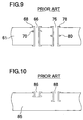
- FIGS. 8(A) to 8(C) and 9 show a structure of a printed circuit board of a multilayer structure where a through-hole is used. More particularly, FIGS. 8(A), 8(B) and 8(C) are top plan views of the first, second and third layers of the printed circuit board, respectively. FIG. 9 is a cross sectional view taken along line X-X of FIG. 8(A).
- the printed circuit board 61 has pads 60, 64 and 74 arranged in rectangular concentrical rows thereon.
- the pads 60 on the outermost row on the first layer allow wiring lines 62 to be led out therefrom toward the outer side of the printed circuit board 61.
- the pads 64 on the middle row are connected to lands 68 of through-holes 66 on the first layer and further connected to wiring lines 72 through lands 70 of the through-holes 66 on the second layer as shown in FIG. 8(B).
- pads 74 on the innermost row of FIG. 8(A) are connected to lands 78 of through-holes 76 on the first layer and further connected to wiring lines 82 through lands 80 of the through-holes 76 on the third layer as shown in FIG. 8(C).
- FIG. 10 shows a cross section of a printed circuit board 85 of a three-layer structure which employs a blind via hole.
- Blind via holes 86 and 88 shown in FIG. 10 interconnect lands of different layers but do not extend through the printed circuit board 85. Such blind via holes are preferable in order to miniaturize an apparatus. Wiring lines are led out from the lands of the different layers in a similar manner as with through-holes.
- a through-hole since it extends through a circuit board, when wiring on a certain layer is considered, no wiring line can be laid at a location at which a through-hole is present. Therefore, there is a problem that a wiring line must be laid bypassing any through-hole.
- a blind via hole a printed circuit board which uses a blind via hole has a unique problem that it requires a greater number of production steps when compared with production of another printed circuit board which employs a through-hole.
- a blind via hole there is a problem that, as the number of inner layers from which wiring lines are to be led out increases, the number of stages (which corresponds to the number of steps for formation of holes) increases and also the cost increases.
- connection method to a printed circuit board for establishing electric connection to a pad embedded together with a wiring line in an inner layer of a printed circuit board of a multilayer structure comprising the steps of removing an insulating material on the pad to form a recessed portion in the printed circuit board to expose the pad through the recessed portion, and connecting a connection member directly to the pad through the recessed portion.
- connection method to a printed circuit board for electrically connecting a connection member of a semiconductor package to a pad embedded together with a wiring line in an inner layer of a printed circuit board of a multilayer structure comprising the steps of removing an insulating material on the pad to form a recessed portion of a depth corresponding to the size of the connection member in the printed circuit board to expose the pad through the recessed portion, and placing the semiconductor package onto the printed circuit board and connecting the connection member directly to the pad through the recessed portion.
- connection structure to a printed circuit board for establishing electric connection to a pad embedded together with a wiring line in an inner layer of a printed circuit board of a multilayer structure, comprising a recessed portion formed on the pad and defined by an insulating material for exposing the pad therethrough, and a connection member connected directly to the pad through the recessed portion.
- connection structure to a printed circuit board for electrically connecting a connection member of a semiconductor package to a pad embedded together with a wiring line in an inner layer of a printed circuit board of a multilayer structure, comprising a recessed portion of a depth corresponding to the size of the connection member formed on the pad in the printed circuit board and defined by an insulating material for exposing the pad therethrough, the connection member arranged on the semiconductor package being connected directly to the pad through the recessed portion.
- connection member preferably is a solder ball or a pin and may be provided on the semiconductor package or some other member.
- Another connection member of the semiconductor package may be connected to another pad provided on the surface of the printed circuit board.
- the recessed portion may be formed by mechanical spot facing of the insulating material or by thermal vaporization of the insulating material by a laser.
- solder balls are arranged in concentrical rows on the semiconductor package, preferably they are arranged such that the diameter increases as the arrangement position comes toward the center of the rows.
- a plurality of pins are arranged in concentric rows on the semiconductor package, preferably they are arranged such that the length increases as the arrangement position comes toward the center of the rows.
- the plurality of solder balls or pins are arranged such that the arrangement pitch thereof increases from the outer row toward the inner row.
- connection member is connected directly to the pad of the inner layer of the printed circuit board of a multilayer structure, the necessity for provision of a through-hole or a blind via hole for wiring to the printed circuit board is eliminated, and wiring is facilitated thereby.
- the semiconductor package to be connected to the printed circuit board has a plurality of solder balls or pins arranged thereon
- wiring to the inner layer is facilitated by arranging the solder balls or the pins such that the diameter of the solder ball or the length of the pin increases as the arrangement position comes toward the center of the rows.
- solder balls or pins are directly connected to pads provided in an inner layer of a printed circuit board through-holes or blind via holes for leading out wiring lines are unnecessary. Since through-holes are unnecessary, the area for wiring lines increases and leading out of wiring lines from a ball grid array or pins is facilitated. Further, while use of a blind via hole results in increase of the number of steps of production of holes as the number of stages increases, with the connection methods, only one step of spot facing is required.
- a wall-shaped insulator As spot facing is performed for each pad of a printed circuit board, a wall-shaped insulator remains around the pad.
- the insulator has an effect of preventing a solder bridge between adjacent pads upon soldering of a ball grid array.
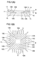
- FIGS. 1(A) to 1(C) shown a printed circuit board of a multilayer structure which employs a ball grid array (BGA) connection to which the present invention is applied.
- BGA ball grid array
- an insulating material located on the pads 12B and 12C embedded in the printed circuit board is removed by mechanical spot facing by a milling machine or spot facing by thermal vaporization by a laser to form such recesses 14B and 14C as shown in FIGS. 1(A) and 1(B) to expose the pads 12B and 12C in the inner layers.
- the recesses 14B and 14C are substantially cylindrical recesses and individually have the same diameters. The diameters are selected so as to be greater than the greatest one of diameters of solder balls provided on a BGA package which is hereinafter described.
- the pads 12A, 12B and 12C have circular shapes of the same size as viewed in the top plan view of FIG. 1(A) and are arranged in a grid-like configuration in an equal pitch.
- walls 16 of the insulating material which forms the printed circuit board 10 remain between the recesses as shown in FIG. 1(C).
- FIGS. 2(A) and 2(B) show a ball grind array (BGA) package to be connected to the printed circuit board 10 of FIGS. 1(A) to 1(C).
- BGA ball grind array
- the BGA package is generally denoted at 22 and includes an array of solder balls arranged in such a manner as shown in FIGS. 2(A) and 2(B) on circular pads 24 of the same size which are arranged in a grid-like configuration in an equal pitch on a package body. It is to be noted that the array of circular pads 24 corresponds in a one-by-one corresponding relationship to the array of the pads 12A, 12B and 12C of the printed circuit board 10.
- solder balls 20A disposed on the outermost row along the four sides of the BGA package 22 solder balls 20B disposed on the middle row along the four sides of the BGA package 22 and solder balls 20C disposed on the innermost row along the four sides of the BGA package 22 have different diameters from one another, and the diameter increases from the outermost row toward the innermost row.
- the diameters of the solder balls are selected in the following manner. In particular, where, in FIG. 1(A), the distance between the top face of a pad 12A and the top face of a pad 12B is represented by A and the distance between the top face of a pad 12B and the top face of a pad 12C is represented by B, if, in FIG.
- FIGS. 2(A) and 2(B) In order to connect the BGA package 22 shown in FIGS. 2(A) and 2(B) to the printed circuit board 10 shown in FIGS. 1(A) to 1(C), cream solder is first applied to the pads 12A, 12B and 12C of the printed circuit board 10, and then the BGA package 22 shown in FIGS. 2(A) and 2(B) is placed onto the printed circuit board 10 such that the tops of the solder balls may directly contact with the corresponding pads 12A, 12B and 12C. Then, solder connection is performed by heating by reflow or the like.
- FIG. 3 shows the printed circuit board 10 and the BGA package 22 in the connected state.
- solder balls 20A in the outermost row of the BGA package 22 are connected to the pads 12A of the printed circuit board 10, and the solder balls 20B in the next row are inserted into the recesses 14B and connected to the pads 12B. Further, the solder balls 20C in the last innermost row are inserted into the recesses 14C and connected to the pads 12C.
- the pads have individually equal sizes and are arranged in a grid-like configuration in an equal pitch.
- the solder balls are formed such that the size decreases toward the outside row, they can be arranged in a decreasing pitch toward the outside row.
- FIG. 4 shows a modified BGA package 22 wherein solder balls are arranged such that the pitch thereof decreases toward the outer row.
- a solder ball on the outermost row is denoted by 20A
- a solder ball on the middle row by 20B is denoted by 20B
- a solder ball on the innermost row by 20C is denoted by 20C
- the pads to which the solder balls are to be connected must be set such that the size decreases toward the outer row.
- the pads are omitted for simplified illustration. According to the arrangement shown in FIG. 4, wiring in a higher density than in the arrangement of FIGS. 1(A) to 1(C) can be achieved.
- a pin may be used in place of a solder ball.
- a pin package is used in place of a BGA package.
- the printed circuit board of a multilayer structure shown in FIGS. 1(A) to 1(C) is used as a printed circuit board to be connected, such a pin package 30 as shown in FIGS. 5(A) and 5(B) may be used.
- the pin package 30 includes a large number of pins 34A, 34B and 34C connected to pads 32 disposed in a grid-like configuration by soldering and so dimensioned that the length increases toward the inner side from the outer side as seen in FIG. 5(B).
- the shortest pins 34A are connected to the pads 32 of the outermost row along the four sides of the pin package 30, and the medium length pins 34B are connected to the pads 32 of the middle row along the four sides of the pin package 30.
- the longest pins 34C are connected to the pads 32 of the innermost row along the four sides of the pin package 30. The lengths of the pins are selected such that, when the pin package 30 of FIGS.
- 5(A) and 5(B) is connected to the printed circuit board 10 of FIGS. 1(A) to 1(C), the ends of the pins 34A, 34B and 34C contact with the pads 12A, 12B and 12C of the printed circuit board 10 as described below.
- FIG. 7 shows a pin 34 (34A, 34B or 34C) soldered to a pad 32.
- a solder fillet 36 is formed at a base portion of the pin 34.
- FIGS. 5(A) and 5(B) In order to connect the pin package 30 shown in FIGS. 5(A) and 5(B) to the printed circuit board 10 shown in FIGS. 1(A) to 1(C), cream solder is applied to the pads 12A, 12B and 12C of the printed circuit board 10, and the pin package 30 shown in FIGS. 5(A) and 5(B) is placed onto the printed circuit board 10. Then, solder connection is performed by heating by reflow or the like.
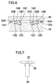
- FIG. 6 shows the printed circuit board 10 and the pin package 30 connected to each other.
- the pins 34A of the pin package 30 are connected directly to the pads 12A of the printed circuit board 10, and the pins 34B are connected directly to the pads 12B. Further, the pins 34C are connected directly to the pads 12C.
Landscapes
- Engineering & Computer Science (AREA)
- Microelectronics & Electronic Packaging (AREA)
- Manufacturing & Machinery (AREA)
- Electric Connection Of Electric Components To Printed Circuits (AREA)
- Production Of Multi-Layered Print Wiring Board (AREA)
Abstract
Description
Claims (28)
- A connection method to a printed circuit board for establishing electric connection to a pad (12B, 12C) embedded together with a wiring line (11) in an inner layer of a printed circuit board (10) of a multilayer structure, characterized in that it comprises the steps of:removing an insulating material on the pad (12B, 12C) to form a recessed portion (14B, 14C) in the printed circuit board (10) to expose the pad (12B, 12C) through the recessed portion (14B, 14C); andconnecting a connection member (20B, 20C; 34B, 34C) directly to the pad (12B, 12C) through the recessed portion (14B, 14C).
- A connection method to a printed circuit board as set forth in claim 1, characterized in that the recessed portion (14B, 14C) is formed by mechanical spot facing of the insulating material.
- A connection method to a printed circuit board as set forth in claim 1, characterized in that the recessed portion (14B, 14C) is formed by thermal vaporization of the insulating material by a laser.
- A connection method to a printed circuit board as set forth in claim 1, 2 or 3, characterized in that the connection member (20B, 20C; 34B, 34C) is connected to the pad (12B, 12C) by soldering.
- A connection method to a printed circuit board as set forth in any one of claims 1 to 4, characterized in that the connection member is a solder ball (20B, 20C).
- A connection method to a printed circuit board as set forth in any one of claims 1 to 4, characterized in that the connection member is a pin (34B, 34C).
- A connection method to a printed circuit board for electrically connecting a connection member (20B, 20C; 34B, 34C) of a semiconductor package (22; 30) to a pad (12B, 12C) embedded together with a wiring line (11) in an inner layer of a printed circuit board (10) of a multilayer structure, characterized in that it comprises the steps of:removing an insulating material on the pad (12B, 12C) to form a recessed portion (14B, 14C) of a depth corresponding to the size of the connection member (20B, 20C; 34B, 34C) in the printed circuit board (10) to expose the pad (12B, 12C) through the recessed portion (14B, 14C); andplacing the semiconductor package (22; 30) onto the printed circuit board (10) and connecting the connection member (20B, 20C; 34B, 34C) directly to the pad (12B, 12C) through the recessed portion (14B, 14C).
- A connection method to a printed circuit board as set forth in claim 7, characterized in that another connection member (20A; 34A) of the semiconductor package (22; 30) is connected to another pad (12A) provided on the surface of the printed circuit board (10).
- A connection method to a printed circuit board as set forth in claim 7 or 8, characterized in that the recessed portion (14B, 14C) is formed by mechanical spot facing of the insulating material.
- A connection method to a printed circuit board as set forth in claim 7 or 8, characterized in that the recessed portion (14B, 14C) is formed by thermal vaporization of the insulating material by a laser.
- A connection method to a printed circuit board as set forth in any one of claims 7 to 10, characterized in that the connection member (20B, 20C; 34B, 34C) is connected to the pad (12B, 12C) by soldering.
- A connection method to a printed circuit board as set forth in any one of claims 7 to 11, characterized in that the connection member is a solder ball (20B, 20C).
- A connection method to a printed circuit board as set forth in any one of claims 7 to 11, characterized in that the connection member is a pin (34B, 34C).
- A connection method to a printed circuit board as set forth in claim 12, characterized in that a plurality of solder balls (20B, 20C) are arranged in concentrical rows on the semiconductor package (22) such that the diameter increases as the arrangement position comes toward the center of the rows.
- A connection method to a printed circuit board as set forth in claim 13, characterized in that a plurality of pins (34B, 34C) are arranged in concentric rows on the semiconductor package (30) such that the length increases as the arrangement position comes toward the center of the rows.
- A connection structure to a printed circuit board for establishing electric connection to a pad (12B, 12C) embedded together with a wiring line (11) in an inner layer of a printed circuit board (10) of a multilayer structure, characterized in that it comprisesa recessed portion (14B, 14C) formed on the pad (12B, 12C) and defined by an insulating material for exposing said pad (12B, 12C) therethrough; anda connection member (20B, 20C; 34B, 34C) connected directly to said pad (12B, 12C) through said recessed portion (14B, 14C).
- A connection structure to a printed circuit board as set forth in claim 16, characterized in that said connection member is a solder ball (20B, 20C).
- A connection structure to a printed circuit board as set forth in claim 16, characterized in that said connection member is a pin (34B, 34C).
- A connection structure to a printed circuit board for electrically connecting a connection member (20B, 20C; 34B, 34C) of a semiconductor package (22; 30) to a pad (12B, 12C) embedded together with a wiring line (11) in an inner layer of a printed circuit board (10) of a multilayer structure, characterized in thata recessed portion (14B, 14C) of a depth corresponding to the size of said connection member (20B, 20C; 34B, 34C) is formed on said pad (12B, 12C) in said printed circuit board (10) and defined by an insulating material for exposing said pad (12B, 12C) therethrough, andsaid connection member (20B, 20C; 34B, 34C) arranged on said semiconductor package (22; 30) is connected directly to said pad (12B, 12C) through said recessed portion (14B, 14C).
- A connection structure to a printed circuit board as set forth in claim 19, characterized in that another connection member (20A; 34A) of said semiconductor package (22; 30) is connected to another pad (12A) provided on the surface of said printed circuit board (10).
- A connection structure to a printed circuit board as set forth in claim 19, characterized in that said connection member is a solder ball (20B, 20C).
- A connection structure to a printed circuit board as set forth in claim 21, characterized in that a plurality of solder balls (20A, 20B, 20C) are arranged in concentrical rows on said semiconductor package (22).
- A connection structure to a printed circuit board as set forth in claim 22, characterized in that said plurality of solder balls (20A, 20B, 20C) are arranged such that the arrangement pitch thereof increases from the outer row toward the inner row.
- A connection structure to a printed circuit board as set forth in claim 22 or 23, characterized in that said plurality of solder balls (20A, 20B, 20C) are arranged such that the diameter increases as the arrangement position comes toward the center of the rows.
- A connection structure to a printed circuit board as set forth in claim 19, characterized in that said connection member is a pin (34B, 34C).
- A connection structure to a printed circuit board as set forth in claim 25, characterized in that a plurality of pins (34A, 34B, 34C) are arranged in concentrical rows on said semiconductor package (30).
- A connection structure to a printed circuit board as set forth in claim 26, characterized in that said plurality of pins (34A, 34B, 34C) are arranged such that the arrangement pitch thereof increases from the outer row toward the inner row.
- A connection structure to a printed circuit board as set forth in claim 26 or 27, characterized in that said plurality of pins (34A, 34B, 34C) are arranged such that the length increases as the arrangement position comes toward the center of the rows.
Applications Claiming Priority (2)
| Application Number | Priority Date | Filing Date | Title |
|---|---|---|---|
| JP11119026A JP2000312075A (en) | 1999-04-27 | 1999-04-27 | Connection method and structure to printed wiring board |
| JP11902699 | 1999-04-27 |
Publications (2)
| Publication Number | Publication Date |
|---|---|
| EP1049162A2 true EP1049162A2 (en) | 2000-11-02 |
| EP1049162A3 EP1049162A3 (en) | 2001-06-27 |
Family
ID=14751156
Family Applications (1)
| Application Number | Title | Priority Date | Filing Date |
|---|---|---|---|
| EP00108979A Withdrawn EP1049162A3 (en) | 1999-04-27 | 2000-04-27 | Interconnection structure of a multilayer circuit board for electrical connection to a semiconductor package and manufacturing method thereof |
Country Status (4)
| Country | Link |
|---|---|
| EP (1) | EP1049162A3 (en) |
| JP (1) | JP2000312075A (en) |
| KR (1) | KR20000071795A (en) |
| CA (1) | CA2305977A1 (en) |
Cited By (7)
| Publication number | Priority date | Publication date | Assignee | Title |
|---|---|---|---|---|
| WO2002035896A1 (en) * | 2000-10-20 | 2002-05-02 | Silverbrook Research Pty. Ltd. | Integrated circuit carrier with recesses |
| EP1478215A3 (en) * | 2003-05-14 | 2006-02-08 | Nortel Networks Limited | Package modification for channel-routed circuit boards |
| US8049325B2 (en) | 2008-11-25 | 2011-11-01 | Samsung Electronics Co., Ltd. | Integrated circuit devices having printed circuit boards therein with staggered bond fingers that support improved electrical isolation |
| US9159670B2 (en) | 2013-08-29 | 2015-10-13 | Qualcomm Incorporated | Ultra fine pitch and spacing interconnects for substrate |
| US9966341B1 (en) | 2016-10-31 | 2018-05-08 | Infineon Technologies Americas Corp. | Input/output pins for chip-embedded substrate |
| CN109791922A (en) * | 2016-08-01 | 2019-05-21 | 赛灵思公司 | The encapsulation of xenogenesis ball pattern |
| CN110248467A (en) * | 2019-06-12 | 2019-09-17 | 惠州市盈帆实业有限公司 | A kind of seamless composite circuit board of pressurized layer and preparation method thereof |
Families Citing this family (4)
| Publication number | Priority date | Publication date | Assignee | Title |
|---|---|---|---|---|
| JP2006120738A (en) * | 2004-10-19 | 2006-05-11 | Murata Mfg Co Ltd | Multilayered ceramic substrate and its manufacturing method |
| KR100607812B1 (en) * | 2004-12-22 | 2006-08-02 | 주식회사 팬택 | Soldering part structure of multilayer FPCB and mobile communication terminal including the same |
| KR101044154B1 (en) * | 2008-12-19 | 2011-06-24 | 삼성전기주식회사 | Printed circuit board having outermost circuit layer embedded under insulating layer and manufacturing method thereof |
| CN112638034B (en) * | 2019-09-24 | 2022-05-27 | 启碁科技股份有限公司 | Electronic device, mainboard thereof and packaging system module |
Family Cites Families (7)
| Publication number | Priority date | Publication date | Assignee | Title |
|---|---|---|---|---|
| JPH04264758A (en) * | 1991-02-20 | 1992-09-21 | Nec Corp | Semiconductor chip carrier |
| US5712192A (en) * | 1994-04-26 | 1998-01-27 | International Business Machines Corporation | Process for connecting an electrical device to a circuit substrate |
| JPH1022643A (en) * | 1996-07-01 | 1998-01-23 | Nippon Avionics Co Ltd | Printed wiring board with cavity, method for manufacturing the same, and manufacturing apparatus |
| US5863812A (en) * | 1996-09-19 | 1999-01-26 | Vlsi Technology, Inc. | Process for manufacturing a multi layer bumped semiconductor device |
| JPH10189656A (en) * | 1996-12-25 | 1998-07-21 | Toshiba Corp | Circuit module, circuit board used for this circuit module, and electronic device mounted with circuit module |
| US5858254A (en) * | 1997-01-28 | 1999-01-12 | International Business Machines Corporation | Multilayered circuitized substrate and method of fabrication |
| JP3580087B2 (en) * | 1997-06-11 | 2004-10-20 | 株式会社デンソー | Electronic component mounting method using bumps |
-
1999
- 1999-04-27 JP JP11119026A patent/JP2000312075A/en active Pending
-
2000
- 2000-04-18 CA CA002305977A patent/CA2305977A1/en not_active Abandoned
- 2000-04-24 KR KR1020000021592A patent/KR20000071795A/en not_active Ceased
- 2000-04-27 EP EP00108979A patent/EP1049162A3/en not_active Withdrawn
Cited By (13)
| Publication number | Priority date | Publication date | Assignee | Title |
|---|---|---|---|---|
| WO2002035896A1 (en) * | 2000-10-20 | 2002-05-02 | Silverbrook Research Pty. Ltd. | Integrated circuit carrier with recesses |
| US7221043B1 (en) | 2000-10-20 | 2007-05-22 | Silverbrook Research Pty Ltd | Integrated circuit carrier with recesses |
| US7402896B2 (en) | 2000-10-20 | 2008-07-22 | Silverbrook Research Pty Ltd | Integrated circuit (IC) carrier assembly incorporating serpentine suspension |
| US7974102B2 (en) | 2000-10-20 | 2011-07-05 | Silverbrook Research Pty Ltd | Integrated circuit carrier assembly |
| EP1478215A3 (en) * | 2003-05-14 | 2006-02-08 | Nortel Networks Limited | Package modification for channel-routed circuit boards |
| US8049325B2 (en) | 2008-11-25 | 2011-11-01 | Samsung Electronics Co., Ltd. | Integrated circuit devices having printed circuit boards therein with staggered bond fingers that support improved electrical isolation |
| US9159670B2 (en) | 2013-08-29 | 2015-10-13 | Qualcomm Incorporated | Ultra fine pitch and spacing interconnects for substrate |
| EP3039716B1 (en) * | 2013-08-29 | 2020-04-08 | Qualcomm Incorporated | Ultra fine pitch and spacing interconnects for substrate |
| CN109791922A (en) * | 2016-08-01 | 2019-05-21 | 赛灵思公司 | The encapsulation of xenogenesis ball pattern |
| US9966341B1 (en) | 2016-10-31 | 2018-05-08 | Infineon Technologies Americas Corp. | Input/output pins for chip-embedded substrate |
| US11101221B2 (en) | 2016-10-31 | 2021-08-24 | Infineon Technologies Americas Corp. | Input/output pins for chip-embedded substrate |
| CN110248467A (en) * | 2019-06-12 | 2019-09-17 | 惠州市盈帆实业有限公司 | A kind of seamless composite circuit board of pressurized layer and preparation method thereof |
| CN110248467B (en) * | 2019-06-12 | 2021-08-13 | 惠州市盈帆实业有限公司 | Composite circuit board and preparation method thereof |
Also Published As
| Publication number | Publication date |
|---|---|
| JP2000312075A (en) | 2000-11-07 |
| CA2305977A1 (en) | 2000-10-27 |
| EP1049162A3 (en) | 2001-06-27 |
| KR20000071795A (en) | 2000-11-25 |
Similar Documents
| Publication | Publication Date | Title |
|---|---|---|
| US5519580A (en) | Method of controlling solder ball size of BGA IC components | |
| JP3308265B2 (en) | IC laminate using flexible circuit with BGA contact | |
| JP3898891B2 (en) | Via plug adapter | |
| JP3111053B2 (en) | Multilayer circuit board with primary and secondary through holes | |
| US5760469A (en) | Semiconductor device and semiconductor device mounting board | |
| US6780023B2 (en) | Printed wiring board having plurality of conductive patterns passing through adjacent pads, circuit component mounted on printed wiring board and circuit module containing wiring board with circuit component mounted thereon | |
| US5657207A (en) | Alignment means for integrated circuit chips | |
| US6528734B2 (en) | Semiconductor device and process for fabricating the same | |
| EP1049162A2 (en) | Interconnection structure of a multilayer circuit board for electrical connection to a semiconductor package and manufacturing method thereof | |
| US7180182B2 (en) | Semiconductor component | |
| US6133134A (en) | Ball grid array integrated circuit package | |
| JP5157455B2 (en) | Semiconductor device | |
| US7420131B2 (en) | Wiring substrate | |
| US5691569A (en) | Integrated circuit package that has a plurality of staggered pins | |
| US8546186B2 (en) | Planar interconnect structure for hybrid circuits | |
| JP2006294976A (en) | Semiconductor device and manufacturing method thereof | |
| KR100620875B1 (en) | Semiconductor device to be mounted on main circuit board and process for manufacturing same device | |
| JPH11163489A (en) | Electronic component mounting structure | |
| JP2001144399A (en) | Board connecting member, electronic circuit board, electronic circuit device, and method of manufacturing electronic circuit device | |
| JPH1167396A (en) | Board with variable terminal pitch | |
| JP2003060113A (en) | Semiconductor device and method of manufacturing the same | |
| JP2005093872A (en) | Lead pin and wiring board with lead pin | |
| JPH11251727A (en) | Method for mounting grid array type semiconductor package | |
| JP2007027341A (en) | Printed wiring board and electronic component mounting structure | |
| JPH07307363A (en) | Semiconductor circuit board |
Legal Events
| Date | Code | Title | Description |
|---|---|---|---|
| PUAI | Public reference made under article 153(3) epc to a published international application that has entered the european phase |
Free format text: ORIGINAL CODE: 0009012 |
|
| AK | Designated contracting states |
Kind code of ref document: A2 Designated state(s): AT BE CH CY DE DK ES FI FR GB GR IE IT LI LU MC NL PT SE |
|
| AX | Request for extension of the european patent |
Free format text: AL;LT;LV;MK;RO;SI |
|
| PUAL | Search report despatched |
Free format text: ORIGINAL CODE: 0009013 |
|
| AK | Designated contracting states |
Kind code of ref document: A3 Designated state(s): AT BE CH CY DE DK ES FI FR GB GR IE IT LI LU MC NL PT SE |
|
| AX | Request for extension of the european patent |
Free format text: AL;LT;LV;MK;RO;SI |
|
| RIC1 | Information provided on ipc code assigned before grant |
Free format text: 7H 01L 23/498 A, 7H 05K 1/11 B, 7H 01L 23/538 B |
|
| 17P | Request for examination filed |
Effective date: 20011005 |
|
| AKX | Designation fees paid |
Free format text: DE FR |
|
| STAA | Information on the status of an ep patent application or granted ep patent |
Free format text: STATUS: THE APPLICATION HAS BEEN WITHDRAWN |
|
| 18W | Application withdrawn |
Withdrawal date: 20020805 |